EP1258929A2 - Semiconductor LED flip-chip having low refractive index underfill - Google Patents
Semiconductor LED flip-chip having low refractive index underfill Download PDFInfo
- Publication number
- EP1258929A2 EP1258929A2 EP02076696A EP02076696A EP1258929A2 EP 1258929 A2 EP1258929 A2 EP 1258929A2 EP 02076696 A EP02076696 A EP 02076696A EP 02076696 A EP02076696 A EP 02076696A EP 1258929 A2 EP1258929 A2 EP 1258929A2
- Authority
- EP
- European Patent Office
- Prior art keywords
- light emitting
- oxides
- emitting structure
- submount
- index
- Prior art date
- Legal status (The legal status is an assumption and is not a legal conclusion. Google has not performed a legal analysis and makes no representation as to the accuracy of the status listed.)
- Granted
Links
Images


Classifications
-
- H—ELECTRICITY
- H10—SEMICONDUCTOR DEVICES; ELECTRIC SOLID-STATE DEVICES NOT OTHERWISE PROVIDED FOR
- H10H—INORGANIC LIGHT-EMITTING SEMICONDUCTOR DEVICES HAVING POTENTIAL BARRIERS
- H10H20/00—Individual inorganic light-emitting semiconductor devices having potential barriers, e.g. light-emitting diodes [LED]
- H10H20/80—Constructional details
- H10H20/85—Packages
- H10H20/852—Encapsulations
- H10H20/854—Encapsulations characterised by their material, e.g. epoxy or silicone resins
-
- H—ELECTRICITY
- H10—SEMICONDUCTOR DEVICES; ELECTRIC SOLID-STATE DEVICES NOT OTHERWISE PROVIDED FOR
- H10W—GENERIC PACKAGES, INTERCONNECTIONS, CONNECTORS OR OTHER CONSTRUCTIONAL DETAILS OF DEVICES COVERED BY CLASS H10
- H10W72/00—Interconnections or connectors in packages
- H10W72/20—Bump connectors, e.g. solder bumps or copper pillars; Dummy bumps; Thermal bumps
-
- H—ELECTRICITY
- H10—SEMICONDUCTOR DEVICES; ELECTRIC SOLID-STATE DEVICES NOT OTHERWISE PROVIDED FOR
- H10H—INORGANIC LIGHT-EMITTING SEMICONDUCTOR DEVICES HAVING POTENTIAL BARRIERS
- H10H20/00—Individual inorganic light-emitting semiconductor devices having potential barriers, e.g. light-emitting diodes [LED]
- H10H20/80—Constructional details
- H10H20/85—Packages
- H10H20/852—Encapsulations
- H10H20/853—Encapsulations characterised by their shape
-
- H—ELECTRICITY
- H10—SEMICONDUCTOR DEVICES; ELECTRIC SOLID-STATE DEVICES NOT OTHERWISE PROVIDED FOR
- H10H—INORGANIC LIGHT-EMITTING SEMICONDUCTOR DEVICES HAVING POTENTIAL BARRIERS
- H10H20/00—Individual inorganic light-emitting semiconductor devices having potential barriers, e.g. light-emitting diodes [LED]
- H10H20/80—Constructional details
- H10H20/85—Packages
- H10H20/857—Interconnections, e.g. lead-frames, bond wires or solder balls
-
- H—ELECTRICITY
- H10—SEMICONDUCTOR DEVICES; ELECTRIC SOLID-STATE DEVICES NOT OTHERWISE PROVIDED FOR
- H10W—GENERIC PACKAGES, INTERCONNECTIONS, CONNECTORS OR OTHER CONSTRUCTIONAL DETAILS OF DEVICES COVERED BY CLASS H10
- H10W72/00—Interconnections or connectors in packages
- H10W72/50—Bond wires
- H10W72/551—Materials of bond wires
- H10W72/552—Materials of bond wires comprising metals or metalloids, e.g. silver
- H10W72/5522—Materials of bond wires comprising metals or metalloids, e.g. silver comprising gold [Au]
-
- H—ELECTRICITY
- H10—SEMICONDUCTOR DEVICES; ELECTRIC SOLID-STATE DEVICES NOT OTHERWISE PROVIDED FOR
- H10W—GENERIC PACKAGES, INTERCONNECTIONS, CONNECTORS OR OTHER CONSTRUCTIONAL DETAILS OF DEVICES COVERED BY CLASS H10
- H10W72/00—Interconnections or connectors in packages
- H10W72/90—Bond pads, in general
-
- H—ELECTRICITY
- H10—SEMICONDUCTOR DEVICES; ELECTRIC SOLID-STATE DEVICES NOT OTHERWISE PROVIDED FOR
- H10W—GENERIC PACKAGES, INTERCONNECTIONS, CONNECTORS OR OTHER CONSTRUCTIONAL DETAILS OF DEVICES COVERED BY CLASS H10
- H10W72/00—Interconnections or connectors in packages
- H10W72/90—Bond pads, in general
- H10W72/921—Structures or relative sizes of bond pads
- H10W72/926—Multiple bond pads having different sizes
-
- H—ELECTRICITY
- H10—SEMICONDUCTOR DEVICES; ELECTRIC SOLID-STATE DEVICES NOT OTHERWISE PROVIDED FOR
- H10W—GENERIC PACKAGES, INTERCONNECTIONS, CONNECTORS OR OTHER CONSTRUCTIONAL DETAILS OF DEVICES COVERED BY CLASS H10
- H10W72/00—Interconnections or connectors in packages
- H10W72/90—Bond pads, in general
- H10W72/931—Shapes of bond pads
- H10W72/936—Multiple bond pads having different shapes
-
- H—ELECTRICITY
- H10—SEMICONDUCTOR DEVICES; ELECTRIC SOLID-STATE DEVICES NOT OTHERWISE PROVIDED FOR
- H10W—GENERIC PACKAGES, INTERCONNECTIONS, CONNECTORS OR OTHER CONSTRUCTIONAL DETAILS OF DEVICES COVERED BY CLASS H10
- H10W72/00—Interconnections or connectors in packages
- H10W72/90—Bond pads, in general
- H10W72/941—Dispositions of bond pads
- H10W72/9415—Dispositions of bond pads relative to the surface, e.g. recessed, protruding
-
- H—ELECTRICITY
- H10—SEMICONDUCTOR DEVICES; ELECTRIC SOLID-STATE DEVICES NOT OTHERWISE PROVIDED FOR
- H10W—GENERIC PACKAGES, INTERCONNECTIONS, CONNECTORS OR OTHER CONSTRUCTIONAL DETAILS OF DEVICES COVERED BY CLASS H10
- H10W72/00—Interconnections or connectors in packages
- H10W72/90—Bond pads, in general
- H10W72/941—Dispositions of bond pads
- H10W72/944—Dispositions of multiple bond pads
-
- H—ELECTRICITY
- H10—SEMICONDUCTOR DEVICES; ELECTRIC SOLID-STATE DEVICES NOT OTHERWISE PROVIDED FOR
- H10W—GENERIC PACKAGES, INTERCONNECTIONS, CONNECTORS OR OTHER CONSTRUCTIONAL DETAILS OF DEVICES COVERED BY CLASS H10
- H10W72/00—Interconnections or connectors in packages
- H10W72/90—Bond pads, in general
- H10W72/941—Dispositions of bond pads
- H10W72/944—Dispositions of multiple bond pads
- H10W72/9445—Top-view layouts, e.g. mirror arrays
-
- H—ELECTRICITY
- H10—SEMICONDUCTOR DEVICES; ELECTRIC SOLID-STATE DEVICES NOT OTHERWISE PROVIDED FOR
- H10W—GENERIC PACKAGES, INTERCONNECTIONS, CONNECTORS OR OTHER CONSTRUCTIONAL DETAILS OF DEVICES COVERED BY CLASS H10
- H10W74/00—Encapsulations, e.g. protective coatings
- H10W74/01—Manufacture or treatment
- H10W74/012—Manufacture or treatment of encapsulations on active surfaces of flip-chip devices, e.g. forming underfills
-
- H—ELECTRICITY
- H10—SEMICONDUCTOR DEVICES; ELECTRIC SOLID-STATE DEVICES NOT OTHERWISE PROVIDED FOR
- H10W—GENERIC PACKAGES, INTERCONNECTIONS, CONNECTORS OR OTHER CONSTRUCTIONAL DETAILS OF DEVICES COVERED BY CLASS H10
- H10W74/00—Encapsulations, e.g. protective coatings
- H10W74/10—Encapsulations, e.g. protective coatings characterised by their shape or disposition
- H10W74/15—Encapsulations, e.g. protective coatings characterised by their shape or disposition on active surfaces of flip-chip devices, e.g. underfills
-
- H—ELECTRICITY
- H10—SEMICONDUCTOR DEVICES; ELECTRIC SOLID-STATE DEVICES NOT OTHERWISE PROVIDED FOR
- H10W—GENERIC PACKAGES, INTERCONNECTIONS, CONNECTORS OR OTHER CONSTRUCTIONAL DETAILS OF DEVICES COVERED BY CLASS H10
- H10W90/00—Package configurations
- H10W90/701—Package configurations characterised by the relative positions of pads or connectors relative to package parts
- H10W90/721—Package configurations characterised by the relative positions of pads or connectors relative to package parts of bump connectors
- H10W90/724—Package configurations characterised by the relative positions of pads or connectors relative to package parts of bump connectors between a chip and a stacked insulating package substrate, interposer or RDL
-
- H—ELECTRICITY
- H10—SEMICONDUCTOR DEVICES; ELECTRIC SOLID-STATE DEVICES NOT OTHERWISE PROVIDED FOR
- H10W—GENERIC PACKAGES, INTERCONNECTIONS, CONNECTORS OR OTHER CONSTRUCTIONAL DETAILS OF DEVICES COVERED BY CLASS H10
- H10W90/00—Package configurations
- H10W90/701—Package configurations characterised by the relative positions of pads or connectors relative to package parts
- H10W90/731—Package configurations characterised by the relative positions of pads or connectors relative to package parts of die-attach connectors
- H10W90/734—Package configurations characterised by the relative positions of pads or connectors relative to package parts of die-attach connectors between a chip and a stacked insulating package substrate, interposer or RDL
Definitions
- LEDs Semiconductor light-emitting diodes
- Materials systems currently of interest in the manufacture of high-brightness LEDs capable of operation across the visible spectrum include Group III-V semiconductors, particularly binary, ternary, and quaternary alloys of gallium, aluminum, indium, and nitrogen, also referred to as III-nitride materials.
- III-nitride devices are epitaxially grown on sapphire, silicon carbide, or III-nitride substrates by metal-organic chemical vapor deposition (MOCVD), molecular beam epitaxy (MBE), or other epitaxial techniques. Some of these substrates are insulating or poorly conducting.
- MOCVD metal-organic chemical vapor deposition
- MBE molecular beam epitaxy
- Devices fabricated from semiconductor crystals grown on such substrates must have both the positive and the negative polarity electrical contacts to the epitaxially-grown semiconductor on the same side of the device.
- semiconductor devices grown on conducting substrates can be fabricated such that one electrical contact is formed on the epitaxially grown material and the other electrical contact is formed on the substrate.
- devices fabricated on conducting substrates may also be designed to have both contacts on the same side of the device on which the epitaxial material is grown in a flip-chip geometry so as to improve light extraction from LED chip, to improve the current-carrying capacity of the chip, or to improve the heat-sinking of the LED die.
- Fig. 1 illustrates a typical III-nitride LED device.
- Semiconductor layers including, for example, n-layer 12, active region 13, and p-layer 14 are epitaxially grown on substrate 11.
- P-contact 15 and n-contact 17 are formed on the same side of the device as described above.
- Electrical isolation between the p-contact 15 and the n-contact 17 is achieved by etching a mesa structure 18 into the device extending from the topmost layer down into the underlying n-layer and forming separate, defined p-contact 15 and n-contact 17.
- the LED is mounted to a submount assembly 22, which typically includes a submount on which the LED is mounted with solder bumps. The solder bumps create a gap between the submount and the LED.
- the connected LED and submount assembly are then typically encapsulated in a high index of refraction gel or epoxy.
- the high index gel or epoxy is selected to match the index of refraction of the sapphire substrate as closely as possible, since the light produced in the device is extracted through the sapphire substrate.
- the difference in index of refraction determines how much light is reflected at that interface, and how much light is transmitted through it. The larger the difference in index of refraction, the more light is reflected.
- the small difference between the index of refraction of the sapphire substrate and the high index gel encapsulating the device ensures that most of the light generated in the device that reaches the emitting surfaces of the sapphire substrate is extracted from the device.
- Photons are generated efficiently within active region 13, but extracting the photons from the semiconductor into the LED package and to the outside world is difficult, in part due to the high indices of refraction of the semiconductor layers. See, for example, Windisch et al., Applied Physics Letters, vol. 74, no. 16, p2256 (1999). Photons generated within the epitaxial semiconductor are incident upon either the interface between the semiconductor and substrate 11, the interface at mesa wall 18 between the semiconductor and the high index gel in submount assembly 22, or the interface between the semiconductor and the metal contacts. Photons incident on any of the three interfaces face a step in material refractive index.
- Such a step in refractive index causes a ray 20 incident on such an interface to be split into a transmitted portion 20a and a reflected portion 20b.
- Light transmitted out from mesa wall 18 i.e. portion 20a
- light lost through transmission at mesa wall 18 contributes to the low light extraction efficiency of semiconductor LEDs.
- the high index gel encapsulating the device results in a small difference in refractive index at the interface at mesa wall 18 between the semiconductor area between the contacts and the submount assembly. As a result, much of the light incident on this area is transmitted in the direction of the submount assembly, which causes significant optical loss. As described above, light extracted in this area towards the submount assembly cannot be usefully extracted from the package; rather, it is incident on the submount where it is absorbed.
- the device area between the contacts on a device such as that shown in Fig. 1 is estimated at 10% of the total area. This area includes the mesa wall and a small portion of semiconductor material parallel to the substrate and between the edge of each contact and the mesa wall.
- Methods of reducing such losses include the use of wafer fabrication techniques such as self-aligned metalization and tightened manufacturing tolerances to reduce the area between the contacts parallel to the substrate. Such wafer fabrication techniques may result in other problems such as increased reliability problems and difficulty in manufacturing. In addition, wafer fabrication techniques do not significantly reduce losses, since 3-D optical ray trace modeling of high index gel-encapsulated, III-nitride LED structures grown on sapphire shows that, of the light undesirably extracted from the LED chip in this direction, the majority is lost through the mesa wall rather than from any surface of the epitaxial material which runs parallel to the substrate surface on which the epitaxial semiconductor was grown. The light extracted at the mesa wall is on the order of 15% of the light generated within the LED, the exact figure depending on, among other factors, the mesa wall height and angle.
- a step in index of refraction is created at the mesa wall of a III-nitride flip chip light emitting device.
- the step in index of refraction reflects much of the light incident on the mesa wall back into the device where it can be usefully extracted.
- a solder wall on the submount or a high index gel or epoxy coating the light emitting device and the submount creates a sealed gap between the light emitting device and the submount.
- the gap is filled with a material having a low index of refraction, such as air, another low index gas, low index flux, or a low index silicone gel or epoxy.
- a high index material covers the substrate of the light emitting device, and a low index material fills the gap between the submount and the light emitting device.
- the high index material may be a silicone gel, epoxy, or a solid high index block
- the low index material may be a different silicone gel, epoxy, or a low index gas such as air.
- Fig. 1 illustrates a flip-chip light emitting diode.
- Fig. 2 illustrates an LED mounted on a submount.
- Fig. 3 is a plan view of an LED showing the location of the p-layer and the n-layer.
- Fig. 4 is a plan view of a submount showing the location of solder bumps and a solder wall.
- Fig. 5 illustrates an LED mounted on a submount and partially encapsulated in a low index material and partially encapsulated in a high index material.
- Fig. 6 illustrates an LED mounted in a high index block.
- Fig. 7 illustrates an LED mounted on a submount and encapsulated in a high index, viscous material.
- Figs. 8A-8C illustrate an embodiment of the present invention.
- Fig. 9 illustrates an example of a mesa wall.
- Fig. 10 illustrates useful light output as a function of mesa wall angle for different devices.
- Fig. 11 illustrates useful light output as a function of mesa wall height for different devices.
- a large step in refractive index is created at the mesa wall separating the p-contact and the n-contact.
- the step in index of refraction is created by placing a material having a low index of refraction at the mesa wall.
- "high” index of refraction refers to an index of refraction greater than or equal to the index of refraction of a material index-matched to sapphire.
- Sapphire has an index of refraction of about 1.7 to 1.8, and materials having indices of refraction as low as 1.5 are considered index-matched to sapphire.
- low index of refraction refers to an index of refraction less than a high index of refraction, e.g. less than about 1.5.
- the large step in refractive index maximizes the light reflected at the mesa wall and minimizes the light transmitted through the mesa wall.
- the light reflected at the mesa wall can then be usefully extracted through the substrate. Any light transmitted at the mesa wall is typically lost.
- the size and shape of the mesa wall are selected to maximize light reflection and minimize light transmission.
- Fig. 2 illustrates a first embodiment of the invention.
- An LED flip chip 32 is mounted epitaxial-layers-down on a submount 34.
- An n-type layer 51 is deposited on a substrate 50.
- An active region 52 is then formed on n-type layer 51, and a p-type layer 53 is formed on the active region.
- a portion of p-type layer 53, active region 52, and n-type layer 51 are etched away to expose a portion of n-type layer 51. The etch leaves mesa wall 56, which allows a p-contact 55 to be connected to p-type layer 53 electrically isolated from n-type layer 51.
- An n-contact 54 connects to the n-layer.
- Fig. 3 illustrates a plan view of the device illustrated in Fig. 2.
- the n-layer 51 encloses p-layer 53. Both p-layer 53 and n-layer 51 include projections which interpose portions of the opposing polarity layer.
- LED 32 is connected to the submount by solder bumps 38, which connect to p-contact 55, and a solder wall 36 which connects to n-contact 54.
- Fig. 4 illustrates the location of solder bumps 38 and solder wall 36 on a submount.
- thick solder bumps 38 and solder wall 36 cause a gap 42 to be formed between the LED and the submount.
- air, nitrogen, a noble gas, forming gas, hydrogen, or another gas with a low index of refraction is trapped in gap 42 between the LED and the submount when the LED is mounted on the submount.
- Forming gas is a mixture of hydrogen and nitrogen often used as a soldering atmosphere. Gasses having high thermal conductivities, such as hydrogen and helium, may specifically be chosen so as to improve thermal transfer between the LED die and the submount, thereby improving the heat-sinking of the LED chip.
- Solder wall 36 encloses gap 42 and prevents the air or other low index gas from escaping.
- the gas fills the space in gap 42, thus the gas is incident on mesa wall 56.
- the layers that make up mesa wall 56, i.e. n-layer 51, active layer 52, and p-layer 53 are all GaN-based materials, and therefore have an index of refraction of about 2.4.
- the air or low index of refraction gas has an index of refraction of about 1.
- the device can then be encapsulated in a high index material, as described above.
- Solder wall 36 prevents any of the high index gel from contacting mesa wall 56.
- Mesa wall 56 may also be coated with a dielectric layer such as alumina, silica, or silicon nitride. Such a structure has a similar result, so long as the dielectric coating is then incident on air or some other low index material.
- a dielectric layer such as alumina, silica, or silicon nitride.
- a low index material such as a low index flux or a low index silicone gel or epoxy is trapped in gap 42.
- Flux is a material used in the process of soldering the LED to the submount.
- Solder bumps 38 and solder wall 36 may be, for example, an alloy of Pb and Sn. When exposed to air, an oxide forms on the surface of solder bumps 38 and solder wall 36. Flux is applied to dissolve the oxide formed on the solder.
- a quantity of low index flux, low index silicone or other gel, or low index epoxy is trapped in gap 42, and prevented from escaping by solder wall 36.
- Solder wall 36 also prevents the high index material encapsulating the device from contaminating the low index material in gap 42.
- Fig. 5 illustrates another embodiment of the present invention.
- no solder wall 36 isolates mesa wall 56 from the outside of the device.
- the n-contacts are connected to the submount by solder bumps 38, similar to the solder bumps connecting the p-contacts to the submount.
- the space between the submount and the LED, up to around the layer of epitaxial material adjacent to the substrate, is filled with a low index gel or low index epoxy 60.
- the low index gel or epoxy suppresses light extraction at the mesa wall towards the submount.
- the remainder of the device, i.e. the substrate is encapsulated in a high index gel or high index epoxy 62, which maximizes light extraction from the substrate.
- the high index gel or epoxy 62 and low index gel or epoxy 60 are selected so that they are viscous enough not to mix at the interface 61 between the low index and high index gels or epoxies.
- the low-index gel or epoxy may be cured to a viscous or hardened state prior to application of the high-index gel or epoxy, thereby reducing the likelihood of intermixing of the low- and high-index materials at the interface between the two materials.
- the entire device may be encapsulated in a single high index gel or epoxy, but the epitaxial side of LED is coated with a material which causes the high index gel or epoxy to react to form a low index material adjacent the lower, epitaxial side of the device.
- Fig. 6 illustrates another embodiment of the present invention.
- the LED 32 is attached to a high index block 64 of solid material.
- High index block 64 is index-matched to the substrate of LED 32, and thereby maximizes light extraction from the substrate.
- High index block 64 replaces the high index gel typically encapsulating the LED mounted on the submount.
- High index block 64 may be shaped so as to further enhance light extraction from the assembly. Since high index block 64 is solid, it does not contact mesa wall 56. LED 32 can therefore be mounted on a submount such that mesa wall 56 is incident on air, thus minimizing light extracted at mesa wall 56.
- High index block 64 may be, for example, oxides of aluminum, tungsten, hafnium, yttrium, and cerium; flourides of cerium, lanthanum, and neodium; high index glass; or zirconia if the LED is formed on a sapphire substrate.
- High index block 64 may be, for example, zinc sulfide, III-nitride materials, SiC, ZnSe and oxides of titanium, zirconium, manganese, chromium, niobium, indium, tin, tantalum, and antimony if the LED is formed on a SiC substrate.
- High index block 64 may be, for example, zinc sulfide, III-nitride materials, SiC, ZnSe and oxides of titanium, zirconium, manganese, chromium, niobium, indium, tin, tantalum, and antimony if the LED is formed on a III-nitride substrate.
- Fig. 7 illustrates another embodiment of the present invention, where the high index gel used to encapsulate the device is extremely viscous.
- the high index material 70 is too viscous to fill the area between LED 32 and submount 34.
- the viscous high index material 70 forms wall 74 between LED 32 and submount 34, which traps a pocket 72 of air or another low index material between LED 32 and submount 34.
- mesa wall 56 is incident on a low index material, thus minimizing the extraction of light at the mesa wall.
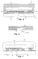
- Figs. 8A-8C illustrate still another embodiment of the present invention.
- a low index material is applied to the mesa wall using dry film technology. Such dry films are available with an index of refraction as low as 1.3.
- Photo-sensitized polypropylene or polyethylene form appropriate polymer dry-films.
- a photo-sensitive polymer dry-film 102 is vacuum-formed onto submount 100. Attached to the submount are solder bumps 108 which are used to attach the LED to the submount.
- the photo-sensitive polymer film 102 is then patterned to remove the film covering the solder bumps, as illustrated in Fig. 8B.
- the photo-sensitive polymer film may be patterned by, for example, applying a photomask over the film and exposing the photomask to dissolve away in a developer solution those portions of the film covering solder bumps 108.
- the film may also be patterned by laser ablation or by patterning the film using standard photoresist, solvents, and/or etchants.
- the LED chip 106 is then located over solder bumps 108 and remaining island of dry-film polymer 102, as illustrated in Fig. 8C.
- the LED and submount are then heated to fuse the solder 108 to the soldering pads 110 of LED 106.
- the polymer dry-film 102 also softens and flows, contacting the LED surface and wetting to the mesa wall.
- the polymer dry-film 102 also wets to the submount wafer 100, forming an impervious layer joining the LED chip to the submount wafer and flowing around the solder connects.
- the film is also chosen so as to serve as a solder mask so that closer spacing between the solder bumps may be obtained than is possible without polymer dry-film; the presence of the mask reduces the probability of solder bridging between adjacent solder bumps.
- each structure creates a large step in index of refraction at the mesa wall, thus each structure improves useful light extraction in the device.
- the structures described above are simple and inexpensive to fabricate, and typically involve little or no additional semiconductor processing.
- the size and shape of mesa wall 56 can be selected to maximize reflection of rays incident on the mesa wall.
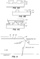
- Fig. 9 illustrates the mesa in more detail.
- the inclination of the mesa wall, ⁇ determines the angle of incidence of a reflected ray on the GaN-substrate interface.
- the angle of incidence is ⁇ .
- ⁇ In order to maximize the probability of extraction of this ray, ⁇ must be as small as possible, and smaller than the critical angle for total internal reflection at the GaN-substrate interface.
- Fig. 10 illustrates the extracted light as a function of mesa wall angle for a device where the mesa wall is incident on a high index material, and for a device according to the present invention where the mesa wall is incident on air.
- Fig. 10 illustrates that considerable enhancement of useful light extraction from the chip can be achieved by selecting a structure having an optimal mesa wall angle. The optimal value of mesa wall angle is dependent on the exact device structure.
- the triangles illustrate a device with a mesa wall incident on air and the diamonds illustrate a device with a mesa wall incident on a high index epoxy.
- a mesa wall angle between 35 and 65 degrees is optimal for useful light extraction from the chip, and the devices with the best useful light extraction have a mesa wall angle between 45 and 55 degrees.
- the mesa wall angle is controlled by tailoring the dry-etch process by which the mesa is defined. Alternatively, an appropriate crystallographic etch could also selectively etch a mesa wall with a particular angle.
- Fig. 11 illustrates the useful light output as a function of mesa wall height for several devices.
- the diamonds illustrate a device with a mesa wall incident on air
- the small squares illustrate a device with a mesa wall incident on a material with an index of refraction of 1.5
- the triangles illustrate a device with a mesa wall incident on a material with an index of refraction of 1.57
- the large squares illustrate a device with a mesa wall incident on a material having an index of refraction of 1.764.
- a chip having a taller mesa has higher useful light extraction. This is because if the mesa wall is highly reflecting, light reflected from the mesa wall escapes the device quickly without attenuation. However, if the mesa wall is incident on a material having a high refractive index, illustrated by the squares, useful light extraction decreases as the mesa height is increased due to increased light extraction through the mesa wall.
- the mesa height is controlled by controlling the depth of the etch into the n-type GaN layer. After etching, enough n-type GaN must remain for formation of a reliable, low resistance n-contact.
Landscapes
- Led Device Packages (AREA)
- Led Devices (AREA)
Abstract
Description
- Semiconductor light-emitting diodes (LEDs) are among the most efficient light sources currently available. Materials systems currently of interest in the manufacture of high-brightness LEDs capable of operation across the visible spectrum include Group III-V semiconductors, particularly binary, ternary, and quaternary alloys of gallium, aluminum, indium, and nitrogen, also referred to as III-nitride materials. Typically, III-nitride devices are epitaxially grown on sapphire, silicon carbide, or III-nitride substrates by metal-organic chemical vapor deposition (MOCVD), molecular beam epitaxy (MBE), or other epitaxial techniques. Some of these substrates are insulating or poorly conducting. Devices fabricated from semiconductor crystals grown on such substrates must have both the positive and the negative polarity electrical contacts to the epitaxially-grown semiconductor on the same side of the device. In contrast, semiconductor devices grown on conducting substrates can be fabricated such that one electrical contact is formed on the epitaxially grown material and the other electrical contact is formed on the substrate. However, devices fabricated on conducting substrates may also be designed to have both contacts on the same side of the device on which the epitaxial material is grown in a flip-chip geometry so as to improve light extraction from LED chip, to improve the current-carrying capacity of the chip, or to improve the heat-sinking of the LED die.
- In order to fabricate efficient LED devices, the contacts must be electrically isolated from each other such that electrical carriers of the appropriate polarity are injected into the p-type and n-type sides of the semiconductor junction, where they recombine to produce light. Fig. 1 illustrates a typical III-nitride LED device. Semiconductor layers, including, for example, n-
layer 12,active region 13, and p-layer 14 are epitaxially grown onsubstrate 11. P-contact 15 and n-contact 17 are formed on the same side of the device as described above. Electrical isolation between the p-contact 15 and the n-contact 17 is achieved by etching amesa structure 18 into the device extending from the topmost layer down into the underlying n-layer and forming separate, defined p-contact 15 and n-contact 17. The LED is mounted to asubmount assembly 22, which typically includes a submount on which the LED is mounted with solder bumps. The solder bumps create a gap between the submount and the LED. The connected LED and submount assembly are then typically encapsulated in a high index of refraction gel or epoxy. - The high index gel or epoxy is selected to match the index of refraction of the sapphire substrate as closely as possible, since the light produced in the device is extracted through the sapphire substrate. When light is incident on an interface between two materials, the difference in index of refraction determines how much light is reflected at that interface, and how much light is transmitted through it. The larger the difference in index of refraction, the more light is reflected. Thus, the small difference between the index of refraction of the sapphire substrate and the high index gel encapsulating the device ensures that most of the light generated in the device that reaches the emitting surfaces of the sapphire substrate is extracted from the device.
- Photons are generated efficiently within
active region 13, but extracting the photons from the semiconductor into the LED package and to the outside world is difficult, in part due to the high indices of refraction of the semiconductor layers. See, for example, Windisch et al., Applied Physics Letters, vol. 74, no. 16, p2256 (1999). Photons generated within the epitaxial semiconductor are incident upon either the interface between the semiconductor andsubstrate 11, the interface atmesa wall 18 between the semiconductor and the high index gel insubmount assembly 22, or the interface between the semiconductor and the metal contacts. Photons incident on any of the three interfaces face a step in material refractive index. Such a step in refractive index causes aray 20 incident on such an interface to be split into a transmittedportion 20a and a reflectedportion 20b. Light transmitted out from mesa wall 18 (i.e. portion 20a) cannot be directed out of the device in a useful direction, thus light lost through transmission atmesa wall 18 contributes to the low light extraction efficiency of semiconductor LEDs. - The high index gel encapsulating the device results in a small difference in refractive index at the interface at
mesa wall 18 between the semiconductor area between the contacts and the submount assembly. As a result, much of the light incident on this area is transmitted in the direction of the submount assembly, which causes significant optical loss. As described above, light extracted in this area towards the submount assembly cannot be usefully extracted from the package; rather, it is incident on the submount where it is absorbed. The device area between the contacts on a device such as that shown in Fig. 1 is estimated at 10% of the total area. This area includes the mesa wall and a small portion of semiconductor material parallel to the substrate and between the edge of each contact and the mesa wall. Methods of reducing such losses include the use of wafer fabrication techniques such as self-aligned metalization and tightened manufacturing tolerances to reduce the area between the contacts parallel to the substrate. Such wafer fabrication techniques may result in other problems such as increased reliability problems and difficulty in manufacturing. In addition, wafer fabrication techniques do not significantly reduce losses, since 3-D optical ray trace modeling of high index gel-encapsulated, III-nitride LED structures grown on sapphire shows that, of the light undesirably extracted from the LED chip in this direction, the majority is lost through the mesa wall rather than from any surface of the epitaxial material which runs parallel to the substrate surface on which the epitaxial semiconductor was grown. The light extracted at the mesa wall is on the order of 15% of the light generated within the LED, the exact figure depending on, among other factors, the mesa wall height and angle. - Accordingly, an LED structure that minimizes optical loss at the mesa wall is needed.
- In accordance with the invention, a step in index of refraction is created at the mesa wall of a III-nitride flip chip light emitting device. The step in index of refraction reflects much of the light incident on the mesa wall back into the device where it can be usefully extracted. In some embodiments, a solder wall on the submount or a high index gel or epoxy coating the light emitting device and the submount creates a sealed gap between the light emitting device and the submount. The gap is filled with a material having a low index of refraction, such as air, another low index gas, low index flux, or a low index silicone gel or epoxy. In other embodiments, a high index material covers the substrate of the light emitting device, and a low index material fills the gap between the submount and the light emitting device. The high index material may be a silicone gel, epoxy, or a solid high index block, and the low index material may be a different silicone gel, epoxy, or a low index gas such as air.
- Fig. 1 illustrates a flip-chip light emitting diode.
- Fig. 2 illustrates an LED mounted on a submount.
- Fig. 3 is a plan view of an LED showing the location of the p-layer and the n-layer.
- Fig. 4 is a plan view of a submount showing the location of solder bumps and a solder wall.
- Fig. 5 illustrates an LED mounted on a submount and partially encapsulated in a low index material and partially encapsulated in a high index material.
- Fig. 6 illustrates an LED mounted in a high index block.
- Fig. 7 illustrates an LED mounted on a submount and encapsulated in a high index, viscous material.
- Figs. 8A-8C illustrate an embodiment of the present invention.
- Fig. 9 illustrates an example of a mesa wall.
- Fig. 10 illustrates useful light output as a function of mesa wall angle for different devices.
- Fig. 11 illustrates useful light output as a function of mesa wall height for different devices.
- In accordance with the invention, a large step in refractive index is created at the mesa wall separating the p-contact and the n-contact. The step in index of refraction is created by placing a material having a low index of refraction at the mesa wall. As used herein, "high" index of refraction refers to an index of refraction greater than or equal to the index of refraction of a material index-matched to sapphire. Sapphire has an index of refraction of about 1.7 to 1.8, and materials having indices of refraction as low as 1.5 are considered index-matched to sapphire. In contrast, "low" index of refraction refers to an index of refraction less than a high index of refraction, e.g. less than about 1.5.
- The large step in refractive index maximizes the light reflected at the mesa wall and minimizes the light transmitted through the mesa wall. The light reflected at the mesa wall can then be usefully extracted through the substrate. Any light transmitted at the mesa wall is typically lost. In addition to creating a large step in refractive index at the mesa wall, the size and shape of the mesa wall are selected to maximize light reflection and minimize light transmission.
- Fig. 2 illustrates a first embodiment of the invention. An
LED flip chip 32 is mounted epitaxial-layers-down on asubmount 34. An n-type layer 51 is deposited on asubstrate 50. Anactive region 52 is then formed on n-type layer 51, and a p-type layer 53 is formed on the active region. A portion of p-type layer 53,active region 52, and n-type layer 51 are etched away to expose a portion of n-type layer 51. The etch leavesmesa wall 56, which allows a p-contact 55 to be connected to p-type layer 53 electrically isolated from n-type layer 51. An n-contact 54 connects to the n-layer. - Fig. 3 illustrates a plan view of the device illustrated in Fig. 2. The n-
layer 51 encloses p-layer 53. Both p-layer 53 and n-layer 51 include projections which interpose portions of the opposing polarity layer. Returning to Fig. 2,LED 32 is connected to the submount bysolder bumps 38, which connect to p-contact 55, and asolder wall 36 which connects to n-contact 54. Fig. 4 illustrates the location of solder bumps 38 andsolder wall 36 on a submount. - When the submount illustrated in Fig. 4 is soldered to the LED illustrated in Fig. 3, thick solder bumps 38 and
solder wall 36 cause agap 42 to be formed between the LED and the submount. In the first embodiment of the invention, air, nitrogen, a noble gas, forming gas, hydrogen, or another gas with a low index of refraction is trapped ingap 42 between the LED and the submount when the LED is mounted on the submount. Forming gas is a mixture of hydrogen and nitrogen often used as a soldering atmosphere. Gasses having high thermal conductivities, such as hydrogen and helium, may specifically be chosen so as to improve thermal transfer between the LED die and the submount, thereby improving the heat-sinking of the LED chip.Solder wall 36 enclosesgap 42 and prevents the air or other low index gas from escaping. The gas fills the space ingap 42, thus the gas is incident onmesa wall 56. The layers that make upmesa wall 56, i.e. n-layer 51,active layer 52, and p-layer 53 are all GaN-based materials, and therefore have an index of refraction of about 2.4. In contrast, the air or low index of refraction gas has an index of refraction of about 1. As a result of the large step in index of refraction atmesa wall 56, most light incident onmesa wall 56 will be reflected back into the LED towardssubstrate 32, where it can be extracted in a useful direction, rather than transmitted intogap 42, where it cannot be extracted in a useful direction. - After the LED is mounted on the submount, trapping air or a low index gas in
gap 42, the device can then be encapsulated in a high index material, as described above.Solder wall 36 prevents any of the high index gel from contactingmesa wall 56. -
Mesa wall 56 may also be coated with a dielectric layer such as alumina, silica, or silicon nitride. Such a structure has a similar result, so long as the dielectric coating is then incident on air or some other low index material. - In another embodiment of the invention, rather than a gas, a low index material such as a low index flux or a low index silicone gel or epoxy is trapped in
gap 42. Flux is a material used in the process of soldering the LED to the submount. Solder bumps 38 andsolder wall 36 may be, for example, an alloy of Pb and Sn. When exposed to air, an oxide forms on the surface of solder bumps 38 andsolder wall 36. Flux is applied to dissolve the oxide formed on the solder. In this embodiment, a quantity of low index flux, low index silicone or other gel, or low index epoxy is trapped ingap 42, and prevented from escaping bysolder wall 36.Solder wall 36 also prevents the high index material encapsulating the device from contaminating the low index material ingap 42. - Fig. 5 illustrates another embodiment of the present invention. In this embodiment, no
solder wall 36 isolatesmesa wall 56 from the outside of the device. The n-contacts are connected to the submount bysolder bumps 38, similar to the solder bumps connecting the p-contacts to the submount. In this embodiment, the space between the submount and the LED, up to around the layer of epitaxial material adjacent to the substrate, is filled with a low index gel orlow index epoxy 60. The low index gel or epoxy suppresses light extraction at the mesa wall towards the submount. The remainder of the device, i.e. the substrate, is encapsulated in a high index gel orhigh index epoxy 62, which maximizes light extraction from the substrate. The high index gel orepoxy 62 and low index gel orepoxy 60 are selected so that they are viscous enough not to mix at theinterface 61 between the low index and high index gels or epoxies. Alternatively, the low-index gel or epoxy may be cured to a viscous or hardened state prior to application of the high-index gel or epoxy, thereby reducing the likelihood of intermixing of the low- and high-index materials at the interface between the two materials. In another embodiment, the entire device may be encapsulated in a single high index gel or epoxy, but the epitaxial side of LED is coated with a material which causes the high index gel or epoxy to react to form a low index material adjacent the lower, epitaxial side of the device. - Fig. 6 illustrates another embodiment of the present invention. After being mounted on the submount, the
LED 32 is attached to ahigh index block 64 of solid material.High index block 64 is index-matched to the substrate ofLED 32, and thereby maximizes light extraction from the substrate.High index block 64 replaces the high index gel typically encapsulating the LED mounted on the submount.High index block 64 may be shaped so as to further enhance light extraction from the assembly. Sincehigh index block 64 is solid, it does not contactmesa wall 56.LED 32 can therefore be mounted on a submount such thatmesa wall 56 is incident on air, thus minimizing light extracted atmesa wall 56.High index block 64 may be, for example, oxides of aluminum, tungsten, hafnium, yttrium, and cerium; flourides of cerium, lanthanum, and neodium; high index glass; or zirconia if the LED is formed on a sapphire substrate.High index block 64 may be, for example, zinc sulfide, III-nitride materials, SiC, ZnSe and oxides of titanium, zirconium, manganese, chromium, niobium, indium, tin, tantalum, and antimony if the LED is formed on a SiC substrate.High index block 64 may be, for example, zinc sulfide, III-nitride materials, SiC, ZnSe and oxides of titanium, zirconium, manganese, chromium, niobium, indium, tin, tantalum, and antimony if the LED is formed on a III-nitride substrate. - Fig. 7 illustrates another embodiment of the present invention, where the high index gel used to encapsulate the device is extremely viscous. In this embodiment, the
high index material 70 is too viscous to fill the area betweenLED 32 andsubmount 34. The viscoushigh index material 70forms wall 74 betweenLED 32 andsubmount 34, which traps apocket 72 of air or another low index material betweenLED 32 andsubmount 34. As a result,mesa wall 56 is incident on a low index material, thus minimizing the extraction of light at the mesa wall. - Figs. 8A-8C illustrate still another embodiment of the present invention. A low index material is applied to the mesa wall using dry film technology. Such dry films are available with an index of refraction as low as 1.3. Photo-sensitized polypropylene or polyethylene form appropriate polymer dry-films. In order to form a light emitting structure with a polymer dry-film low index material on the mesa wall, first a photo-sensitive polymer dry-
film 102 is vacuum-formed ontosubmount 100. Attached to the submount aresolder bumps 108 which are used to attach the LED to the submount. The photo-sensitive polymer film 102 is then patterned to remove the film covering the solder bumps, as illustrated in Fig. 8B. The photo-sensitive polymer film may be patterned by, for example, applying a photomask over the film and exposing the photomask to dissolve away in a developer solution those portions of the film covering solder bumps 108. The film may also be patterned by laser ablation or by patterning the film using standard photoresist, solvents, and/or etchants. - The
LED chip 106 is then located over solder bumps 108 and remaining island of dry-film polymer 102, as illustrated in Fig. 8C. The LED and submount are then heated to fuse thesolder 108 to thesoldering pads 110 ofLED 106. In the process, the polymer dry-film 102 also softens and flows, contacting the LED surface and wetting to the mesa wall. The polymer dry-film 102 also wets to thesubmount wafer 100, forming an impervious layer joining the LED chip to the submount wafer and flowing around the solder connects. - The film is also chosen so as to serve as a solder mask so that closer spacing between the solder bumps may be obtained than is possible without polymer dry-film; the presence of the mask reduces the probability of solder bridging between adjacent solder bumps.
- The structures described in Figs. 2-8C may offer several advantages. Each structure creates a large step in index of refraction at the mesa wall, thus each structure improves useful light extraction in the device. In addition, the structures described above are simple and inexpensive to fabricate, and typically involve little or no additional semiconductor processing.
- The size and shape of
mesa wall 56 can be selected to maximize reflection of rays incident on the mesa wall. Fig. 9 illustrates the mesa in more detail. The inclination of the mesa wall, µ, determines the angle of incidence of a reflected ray on the GaN-substrate interface. The angle of incidence is π. In order to maximize the probability of extraction of this ray, π must be as small as possible, and smaller than the critical angle for total internal reflection at the GaN-substrate interface. - Fig. 10 illustrates the extracted light as a function of mesa wall angle for a device where the mesa wall is incident on a high index material, and for a device according to the present invention where the mesa wall is incident on air. Fig. 10 illustrates that considerable enhancement of useful light extraction from the chip can be achieved by selecting a structure having an optimal mesa wall angle. The optimal value of mesa wall angle is dependent on the exact device structure. The triangles illustrate a device with a mesa wall incident on air and the diamonds illustrate a device with a mesa wall incident on a high index epoxy. For a device with a mesa wall incident on air, a mesa wall angle between 35 and 65 degrees is optimal for useful light extraction from the chip, and the devices with the best useful light extraction have a mesa wall angle between 45 and 55 degrees. The mesa wall angle is controlled by tailoring the dry-etch process by which the mesa is defined. Alternatively, an appropriate crystallographic etch could also selectively etch a mesa wall with a particular angle.
- The optimal height of the mesa wall is also dependent on the structure of the LED chip. Fig. 11 illustrates the useful light output as a function of mesa wall height for several devices. The diamonds illustrate a device with a mesa wall incident on air, the small squares illustrate a device with a mesa wall incident on a material with an index of refraction of 1.5, the triangles illustrate a device with a mesa wall incident on a material with an index of refraction of 1.57, and the large squares illustrate a device with a mesa wall incident on a material having an index of refraction of 1.764. For a chip having an optimally angled mesa wall incident on a low index material, a chip having a taller mesa has higher useful light extraction. This is because if the mesa wall is highly reflecting, light reflected from the mesa wall escapes the device quickly without attenuation. However, if the mesa wall is incident on a material having a high refractive index, illustrated by the squares, useful light extraction decreases as the mesa height is increased due to increased light extraction through the mesa wall. The mesa height is controlled by controlling the depth of the etch into the n-type GaN layer. After etching, enough n-type GaN must remain for formation of a reliable, low resistance n-contact.
- While particular embodiments of the present invention have been shown and described, it will be obvious to those skilled in the art that changes and modifications may be made without departing from the invention in its broader aspects and, therefore, the appended claims are to encompass within their scope all such changes and modifications as fall within the true spirit and scope of this invention. For example, the invention is not limited to a GaN-based device as described above.
Claims (24)
- A light emitting structure, comprising:a III-nitride light emitting device, the light emitting device comprising:a substrate;an n-type layer overlying the substrate;an active region overlying the n-type layer;a p-type layer overlying the active region;an n-contact connected to the n-type layer; anda p-contact connected to the p-type layer, wherein the n-contact and the p-contact are formed on the same side of the device and the n-contact is separated from the p-contact by a mesa wall;a submount, connected to the light emitting device;a gap between the III-nitride light emitting device and the submount; anda quantity of material in the gap, wherein the quantity of material is incident on the mesa wall and has a low index of refraction.
- The light emitting structure of Claim 1 wherein the gap between the III-nitride light emitting device and the submount is sealed by an outer solder wall disposed on the submount, and wherein the submount is connected to the III-nitride light emitting device by the outer solder wall.
- The light emitting structure of Claim 1 further comprising a gel deposited over a portion of the light emitting device and the submount, wherein the gap between the III-nitride light emitting device and the submount is sealed off by the gel.
- The light emitting structure of Claim 1 wherein the material is a gas.
- The light emitting structure of Claim 4 wherein the gas is selected from the group consisting of air, nitrogen, hydrogen, helium, neon, argon, krypton, and xenon.
- The light emitting structure of Claim 4 wherein the gas is a forming gas.
- The light emitting structure of Claim 1 wherein the material is a silicone gel.
- The light emitting structure of Claim 1 wherein the material is flux.
- The light emitting structure of Claim 1 wherein the light emitting device further comprises a dielectric layer formed over the mesa wall.
- The light emitting structure of Claim 1 wherein the material is epoxy.
- The light emitting structure of Claim 1 wherein the material has an index of refraction between about 1 and 1.5.
- The light emitting structure of Claim 1 wherein the material is an organic polymer.
- The light emitting structure of Claim 1 wherein the material is a polymer dry-film.
- The light emitting structure of Claim 1 wherein the mesa wall forms an angle with the substrate between 35 and 65 degrees.
- The light emitting structure of Claim 1 wherein the mesa wall forms an angle with the substrate between about 45 and 55 degrees.
- The light emitting structure of Claim 1 wherein the mesa wall has a height between about 1 and 4 µm.
- A light emitting structure, comprising:wherein the first index of refraction is greater than the second index of refraction.a III-nitride light emitting device, the light emitting device comprising:a substrate;an n-type layer overlying the substrate;an active region overlying the n-type layer;a p-type layer overlying the active region;an n-contact connected to the n-type layer; anda p-contact connected to the p-type layer, wherein the n-contact and the p-contact are formed on the same side of the device and the n-contact is separated from the p-contact by a mesa wall;a submount connected to the III-nitride light emitting device such that a gap is present between the submount and the III-nitride light emitting device;a first quantity of material having a first index of refraction, the first quantity of material covering the substrate of the III-nitride light emitting device; anda second quantity of material having a second index of refraction, the second quantity of material being disposed in the gap between the submount and the light emitting device and being incident on the mesa wall;
- The light emitting structure of Claim 17 wherein the first quantity of material is a first silicone gel and the second quantity of material is a second silicone gel.
- The light emitting structure of Claim 17 wherein the first quantity of material is a first epoxy and the second quantity of the material is a second epoxy.
- The light emitting structure of Claim 17 wherein the first quantity of material is one of a silicone gel and an epoxy and the second quantity of material is the other of a silicone gel and an epoxy.
- The light emitting structure of Claim 17 wherein the first quantity of material is a solid block of material and the second quantity of material is a gas.
- The light emitting structure of Claim 17 wherein the substrate is sapphire and the first quantity of material is selected from the group consisting of oxides of aluminum, oxides of tungsten, oxides of hafnium, oxides of yttrium, oxides of cerium, fluorides of cerium, fluorides of lanthanum, fluorides of neodium, high index glass, and zirconia.
- The light emitting structure of Claim 17 wherein the substrate is SiC and the first quantity of material is selected from the group consisting of zinc sulfide, III-nitride materials, SiC, ZnSe, oxides of titanium, oxides of zirconium, oxides of manganese, oxides of chromium, oxides of niobium, oxides of indium, oxides of tin, oxides of tantalum, and oxides of antimony.
- The light emitting structure Claim 17 wherein the substrate is a III-nitride material and the first quantity of material is selected from the group consisting of zinc sulfide, III-nitride materials, SiC, ZnSe, oxides of titanium, oxides of zirconium, oxides of manganese, oxides of chromium, oxides of niobium, oxides of indium, oxides of tin, oxides of tantalum, and oxides of antimony.
Applications Claiming Priority (2)
| Application Number | Priority Date | Filing Date | Title |
|---|---|---|---|
| US858833 | 2001-05-15 | ||
| US09/858,833 US6455878B1 (en) | 2001-05-15 | 2001-05-15 | Semiconductor LED flip-chip having low refractive index underfill |
Publications (3)
| Publication Number | Publication Date |
|---|---|
| EP1258929A2 true EP1258929A2 (en) | 2002-11-20 |
| EP1258929A3 EP1258929A3 (en) | 2008-09-10 |
| EP1258929B1 EP1258929B1 (en) | 2015-12-02 |
Family
ID=25329309
Family Applications (1)
| Application Number | Title | Priority Date | Filing Date |
|---|---|---|---|
| EP02076696.0A Expired - Lifetime EP1258929B1 (en) | 2001-05-15 | 2002-04-29 | Semiconductor LED flip-chip having low refractive index underfill |
Country Status (4)
| Country | Link |
|---|---|
| US (1) | US6455878B1 (en) |
| EP (1) | EP1258929B1 (en) |
| JP (1) | JP4488669B2 (en) |
| TW (1) | TW541729B (en) |
Cited By (2)
| Publication number | Priority date | Publication date | Assignee | Title |
|---|---|---|---|---|
| EP2262017A3 (en) * | 2001-07-23 | 2017-01-04 | Cree, Inc. | Flip-Chip bonding of light emitting devices and light emitting devices suitable for Flip-Chip bonding |
| US9620691B2 (en) | 2014-08-22 | 2017-04-11 | Lg Innotek Co., Ltd. | Light emitting device package |
Families Citing this family (80)
| Publication number | Priority date | Publication date | Assignee | Title |
|---|---|---|---|---|
| US7547921B2 (en) * | 2000-08-08 | 2009-06-16 | Osram Opto Semiconductors Gmbh | Semiconductor chip for optoelectronics |
| US20020017652A1 (en) * | 2000-08-08 | 2002-02-14 | Stefan Illek | Semiconductor chip for optoelectronics |
| JP3764640B2 (en) * | 2000-09-26 | 2006-04-12 | 京セラ株式会社 | Optical module and manufacturing method thereof |
| US6791119B2 (en) | 2001-02-01 | 2004-09-14 | Cree, Inc. | Light emitting diodes including modifications for light extraction |
| US6794684B2 (en) | 2001-02-01 | 2004-09-21 | Cree, Inc. | Reflective ohmic contacts for silicon carbide including a layer consisting essentially of nickel, methods of fabricating same, and light emitting devices including the same |
| US6630689B2 (en) * | 2001-05-09 | 2003-10-07 | Lumileds Lighting, U.S. Llc | Semiconductor LED flip-chip with high reflectivity dielectric coating on the mesa |
| US6740906B2 (en) * | 2001-07-23 | 2004-05-25 | Cree, Inc. | Light emitting diodes including modifications for submount bonding |
| US7211833B2 (en) | 2001-07-23 | 2007-05-01 | Cree, Inc. | Light emitting diodes including barrier layers/sublayers |
| EP1286194A3 (en) * | 2001-08-21 | 2004-05-19 | Canon Kabushiki Kaisha | Optical waveguide apparatus |
| US6878973B2 (en) * | 2001-08-23 | 2005-04-12 | Lumileds Lighting U.S., Llc | Reduction of contamination of light emitting devices |
| US20030090103A1 (en) * | 2001-11-09 | 2003-05-15 | Thomas Becker | Direct mailing device |
| JP3833132B2 (en) * | 2002-03-25 | 2006-10-11 | キヤノン株式会社 | Manufacturing method of optical waveguide device |
| KR100894651B1 (en) * | 2002-07-08 | 2009-04-24 | 엘지디스플레이 주식회사 | Active matrix organic electroluminescent display panel and manufacturing method thereof |
| JP4143732B2 (en) * | 2002-10-16 | 2008-09-03 | スタンレー電気株式会社 | In-vehicle wavelength converter |
| US7213942B2 (en) * | 2002-10-24 | 2007-05-08 | Ac Led Lighting, L.L.C. | Light emitting diodes for high AC voltage operation and general lighting |
| US6957899B2 (en) * | 2002-10-24 | 2005-10-25 | Hongxing Jiang | Light emitting diodes for high AC voltage operation and general lighting |
| KR100512361B1 (en) * | 2002-12-09 | 2005-09-02 | 엘지이노텍 주식회사 | Large-size flip chip led having ring-type mesa geometry |
| US6977396B2 (en) * | 2003-02-19 | 2005-12-20 | Lumileds Lighting U.S., Llc | High-powered light emitting device with improved thermal properties |
| RU2231171C1 (en) * | 2003-04-30 | 2004-06-20 | Закрытое акционерное общество "Инновационная фирма "ТЕТИС" | Light-emitting diode |
| JP2006525669A (en) * | 2003-05-02 | 2006-11-09 | ユニバーシティ・カレッジ・コークーナショナル・ユニバーシティ・オブ・アイルランド,コーク | Light emitting diode and manufacturing method thereof |
| US6987304B2 (en) * | 2003-05-07 | 2006-01-17 | Honeywell International Inc. | Methods and apparatus for particle reduction in MEMS devices |
| US6969874B1 (en) | 2003-06-12 | 2005-11-29 | Sandia Corporation | Flip-chip light emitting diode with resonant optical microcavity |
| KR100568269B1 (en) * | 2003-06-23 | 2006-04-05 | 삼성전기주식회사 | Gallium nitride based light emitting diode for flip-chip bonding and manufacturing method thereof |
| JP4580633B2 (en) * | 2003-11-14 | 2010-11-17 | スタンレー電気株式会社 | Semiconductor device and manufacturing method thereof |
| CN100375300C (en) * | 2003-11-25 | 2008-03-12 | 葛世潮 | high power light emitting diode |
| US20050133806A1 (en) * | 2003-12-17 | 2005-06-23 | Hui Peng | P and N contact pad layout designs of GaN based LEDs for flip chip packaging |
| US20050161779A1 (en) * | 2004-01-26 | 2005-07-28 | Hui Peng | Flip chip assemblies and lamps of high power GaN LEDs, wafer level flip chip package process, and method of fabricating the same |
| CN100423298C (en) * | 2004-02-27 | 2008-10-01 | 沈育浓 | Light emitting diode chip package and packaging method thereof |
| JP5005164B2 (en) * | 2004-03-03 | 2012-08-22 | 株式会社ジャパンディスプレイイースト | LIGHT EMITTING ELEMENT, LIGHT EMITTING DISPLAY DEVICE AND LIGHTING DEVICE |
| US7285801B2 (en) * | 2004-04-02 | 2007-10-23 | Lumination, Llc | LED with series-connected monolithically integrated mesas |
| US20050253283A1 (en) * | 2004-05-13 | 2005-11-17 | Dcamp Jon B | Getter deposition for vacuum packaging |
| JP4632697B2 (en) * | 2004-06-18 | 2011-02-16 | スタンレー電気株式会社 | Semiconductor light emitting device and manufacturing method thereof |
| US7033864B2 (en) * | 2004-09-03 | 2006-04-25 | Texas Instruments Incorporated | Grooved substrates for uniform underfilling solder ball assembled electronic devices |
| ATE537564T1 (en) * | 2004-10-13 | 2011-12-15 | Panasonic Corp | LUMINESCENT LIGHT SOURCE, METHOD FOR PRODUCING SAME AND LIGHT EMITTING DEVICE |
| US7679097B2 (en) | 2004-10-21 | 2010-03-16 | Nichia Corporation | Semiconductor light emitting device and method for manufacturing the same |
| JP4634810B2 (en) * | 2005-01-20 | 2011-02-16 | 信越化学工業株式会社 | Silicone sealed LED |
| US7525248B1 (en) | 2005-01-26 | 2009-04-28 | Ac Led Lighting, L.L.C. | Light emitting diode lamp |
| US7535028B2 (en) * | 2005-02-03 | 2009-05-19 | Ac Led Lighting, L.Lc. | Micro-LED based high voltage AC/DC indicator lamp |
| KR100597166B1 (en) * | 2005-05-03 | 2006-07-04 | 삼성전기주식회사 | Flip Chip Light Emitting Diode and Manufacturing Method Thereof |
| DE102005024830B4 (en) * | 2005-05-27 | 2009-07-02 | Noctron S.A.R.L. | Light emitting diode array |
| US8272757B1 (en) | 2005-06-03 | 2012-09-25 | Ac Led Lighting, L.L.C. | Light emitting diode lamp capable of high AC/DC voltage operation |
| US7754507B2 (en) * | 2005-06-09 | 2010-07-13 | Philips Lumileds Lighting Company, Llc | Method of removing the growth substrate of a semiconductor light emitting device |
| US7736945B2 (en) * | 2005-06-09 | 2010-06-15 | Philips Lumileds Lighting Company, Llc | LED assembly having maximum metal support for laser lift-off of growth substrate |
| WO2006137711A1 (en) * | 2005-06-22 | 2006-12-28 | Seoul Opto-Device Co., Ltd. | Light emitting device and method of manufacturing the same |
| TWI257722B (en) * | 2005-07-15 | 2006-07-01 | Ind Tech Res Inst | Package structure of light-emitting diode with electrothermal component |
| FR2890065B1 (en) * | 2005-08-30 | 2007-09-21 | Commissariat Energie Atomique | METHOD FOR ENCAPSULATING A COMPONENT, ESPECIALLY ELECTRIC OR ELECTRONIC, BY MEANS OF AN IMPROVED WELDING CORD |
| US20070114643A1 (en) * | 2005-11-22 | 2007-05-24 | Honeywell International Inc. | Mems flip-chip packaging |
| US7491567B2 (en) * | 2005-11-22 | 2009-02-17 | Honeywell International Inc. | MEMS device packaging methods |
| JP4777757B2 (en) * | 2005-12-01 | 2011-09-21 | スタンレー電気株式会社 | Semiconductor light emitting device and manufacturing method thereof |
| DE102006015606A1 (en) * | 2006-04-04 | 2007-10-18 | Noctron Holding S.A. | Semiconductor lamps and light panels with such |
| DE102006049081B4 (en) * | 2006-10-13 | 2012-06-14 | Noctron Soparfi S.A. | Semiconductor lamps and light panels with such |
| TWI349146B (en) * | 2006-05-15 | 2011-09-21 | Epistar Corp | A light-mixing type light-emitting device |
| US8062925B2 (en) * | 2006-05-16 | 2011-11-22 | Koninklijke Philips Electronics N.V. | Process for preparing a semiconductor light-emitting device for mounting |
| US9111950B2 (en) * | 2006-09-28 | 2015-08-18 | Philips Lumileds Lighting Company, Llc | Process for preparing a semiconductor structure for mounting |
| US7714348B2 (en) * | 2006-10-06 | 2010-05-11 | Ac-Led Lighting, L.L.C. | AC/DC light emitting diodes with integrated protection mechanism |
| CN101226972B (en) * | 2007-01-16 | 2011-01-12 | 台达电子工业股份有限公司 | Light emitting diode device and manufacturing method thereof |
| DE102008005344A1 (en) * | 2007-09-21 | 2009-04-02 | Osram Opto Semiconductors Gmbh | Radiation-emitting component |
| US7985979B2 (en) | 2007-12-19 | 2011-07-26 | Koninklijke Philips Electronics, N.V. | Semiconductor light emitting device with light extraction structures |
| TWI422058B (en) * | 2008-03-04 | 2014-01-01 | 億光電子工業股份有限公司 | Light-emitting diode package structure and manufacturing method thereof |
| US20110114970A1 (en) * | 2008-04-23 | 2011-05-19 | Agency For Science, Technology And Research | Light emitting diode structure, a lamp device and a method of forming a light emitting diode structure |
| DE102008038750A1 (en) * | 2008-08-12 | 2010-02-18 | Osram Opto Semiconductors Gmbh | Optoelectronic component and method for its production |
| US7875984B2 (en) * | 2009-03-04 | 2011-01-25 | Koninklijke Philips Electronics N.V. | Complaint bonding structures for semiconductor devices |
| US8202741B2 (en) * | 2009-03-04 | 2012-06-19 | Koninklijke Philips Electronics N.V. | Method of bonding a semiconductor device using a compliant bonding structure |
| US8089091B2 (en) * | 2009-06-18 | 2012-01-03 | Koninklijke Philips Electronics N.V. | Semiconductor light emitting device with a contact formed on a textured surface |
| US20140077246A1 (en) * | 2011-06-01 | 2014-03-20 | Koninklijke Philips N.V. | Light emitting device bonded to a support substrate |
| DE102013103079A1 (en) * | 2013-03-26 | 2014-10-02 | Osram Opto Semiconductors Gmbh | Optoelectronic semiconductor chip and method for producing an optoelectronic semiconductor chip |
| US9299899B2 (en) | 2013-07-23 | 2016-03-29 | Grote Industries, Llc | Flexible lighting device having unobtrusive conductive layers |
| WO2015011586A1 (en) * | 2013-07-26 | 2015-01-29 | Koninklijke Philips N.V. | Led dome with inner high index pillar |
| KR102140273B1 (en) * | 2014-01-08 | 2020-07-31 | 엘지이노텍 주식회사 | Light emitting device and light emitting device package including the same |
| US9257622B2 (en) * | 2014-04-14 | 2016-02-09 | Jin-Ywan Lin | Light-emitting structure |
| KR102464324B1 (en) * | 2015-10-27 | 2022-11-09 | 쑤저우 레킨 세미컨덕터 컴퍼니 리미티드 | Light emitting device package, manufacturing method thereof and light system having the same |
| EP3370266B1 (en) * | 2015-10-29 | 2020-06-17 | Kyocera Corporation | Light-emitting element, light receiving and emitting element module, and optical sensor |
| KR102550005B1 (en) * | 2016-07-15 | 2023-07-03 | 서울바이오시스 주식회사 | Uv light emitting diode |
| KR102657114B1 (en) * | 2017-02-10 | 2024-04-15 | 주식회사 루멘스 | micro LED module and method for fabricating the same |
| EP3561870A4 (en) * | 2016-12-23 | 2020-11-25 | Lumens Co., Ltd. | MICRO LED MODULE AND MANUFACTURING PROCESS FOR IT |
| JP6555247B2 (en) * | 2016-12-28 | 2019-08-07 | 日亜化学工業株式会社 | Light emitting device and manufacturing method thereof |
| KR102422386B1 (en) * | 2017-04-21 | 2022-07-20 | 주식회사 루멘스 | Micro led display apparatus and method for fabricating the same |
| KR102305180B1 (en) * | 2017-04-25 | 2021-09-28 | 주식회사 루멘스 | Micro led display apparatus and method for fabricating the same |
| KR20200054747A (en) * | 2018-11-12 | 2020-05-20 | 삼성전자주식회사 | Display module, display apparatus including the same and method of manufacturing display module |
| DE102021129113A1 (en) * | 2021-11-09 | 2023-05-11 | OSRAM Opto Semiconductors Gesellschaft mit beschränkter Haftung | SEMICONDUCTOR CHIP AND COMPONENT |
Citations (6)
| Publication number | Priority date | Publication date | Assignee | Title |
|---|---|---|---|---|
| EP0415640A2 (en) | 1989-08-29 | 1991-03-06 | Hewlett-Packard Company | High efficiency lamp or light accepter |
| JPH06177429A (en) | 1992-12-08 | 1994-06-24 | Nichia Chem Ind Ltd | Blue LED element |
| US5557115A (en) | 1994-08-11 | 1996-09-17 | Rohm Co. Ltd. | Light emitting semiconductor device with sub-mount |
| EP0905797A2 (en) | 1997-09-29 | 1999-03-31 | Siemens Aktiengesellschaft | Semiconductor light source and method of fabrication |
| EP0921577A1 (en) | 1997-01-31 | 1999-06-09 | Matsushita Electronics Corporation | Light emitting element, semiconductor light emitting device, and method for manufacturing them |
| JP2000244012A (en) | 1998-12-22 | 2000-09-08 | Toyoda Gosei Co Ltd | Method for manufacturing group III nitride compound semiconductor device |
Family Cites Families (24)
| Publication number | Priority date | Publication date | Assignee | Title |
|---|---|---|---|---|
| JPH0541158U (en) * | 1991-10-31 | 1993-06-01 | 日本ビクター株式会社 | Light emitting device |
| JP3423328B2 (en) * | 1991-12-09 | 2003-07-07 | 豊田合成株式会社 | Gallium nitride based compound semiconductor light emitting device |
| JPH0563068U (en) * | 1992-01-31 | 1993-08-20 | シャープ株式会社 | Resin-sealed light emitter |
| JPH05327012A (en) * | 1992-05-15 | 1993-12-10 | Sanyo Electric Co Ltd | Silicon Carbide Light Emitting Diode |
| JPH0637143A (en) | 1992-07-15 | 1994-02-10 | Toshiba Corp | Semiconductor device and method of manufacturing semiconductor device |
| US6404127B2 (en) * | 1993-07-20 | 2002-06-11 | University Of Georgia Research Foundation, Inc. | Multi-color microcavity resonant display |
| JP3646732B2 (en) * | 1994-08-11 | 2005-05-11 | ローム株式会社 | Semiconductor light emitting device with filter |
| US5585648A (en) * | 1995-02-03 | 1996-12-17 | Tischler; Michael A. | High brightness electroluminescent device, emitting in the green to ultraviolet spectrum, and method of making the same |
| US5661074A (en) * | 1995-02-03 | 1997-08-26 | Advanced Technology Materials, Inc. | High brightness electroluminescent device emitting in the green to ultraviolet spectrum and method of making the same |
| US5670798A (en) * | 1995-03-29 | 1997-09-23 | North Carolina State University | Integrated heterostructures of Group III-V nitride semiconductor materials including epitaxial ohmic contact non-nitride buffer layer and methods of fabricating same |
| US5679965A (en) * | 1995-03-29 | 1997-10-21 | North Carolina State University | Integrated heterostructures of Group III-V nitride semiconductor materials including epitaxial ohmic contact, non-nitride buffer layer and methods of fabricating same |
| US5739554A (en) * | 1995-05-08 | 1998-04-14 | Cree Research, Inc. | Double heterojunction light emitting diode with gallium nitride active layer |
| US5625202A (en) * | 1995-06-08 | 1997-04-29 | University Of Central Florida | Modified wurtzite structure oxide compounds as substrates for III-V nitride compound semiconductor epitaxial thin film growth |
| WO1998033212A1 (en) * | 1997-01-23 | 1998-07-30 | Seiko Epson Corporation | Film carrier tape, semiconductor assembly, semiconductor device, manufacturing method therefor, mounting board, and electronic equipment |
| US6229160B1 (en) * | 1997-06-03 | 2001-05-08 | Lumileds Lighting, U.S., Llc | Light extraction from a semiconductor light-emitting device via chip shaping |
| US5919329A (en) * | 1997-10-14 | 1999-07-06 | Gore Enterprise Holdings, Inc. | Method for assembling an integrated circuit chip package having at least one semiconductor device |
| JP3819143B2 (en) * | 1998-03-24 | 2006-09-06 | 日本オプネクスト株式会社 | Optical coupling system, optical module, and optical transmission system |
| JP3531475B2 (en) * | 1998-05-22 | 2004-05-31 | 日亜化学工業株式会社 | Flip chip type optical semiconductor device |
| JP2000049387A (en) * | 1998-07-27 | 2000-02-18 | Matsushita Electron Corp | Semiconductor light emitting device |
| JP2000208822A (en) * | 1999-01-11 | 2000-07-28 | Matsushita Electronics Industry Corp | Semiconductor light emitting device |
| JP3632507B2 (en) * | 1999-07-06 | 2005-03-23 | 日亜化学工業株式会社 | Light emitting device |
| JP2001036149A (en) * | 1999-07-23 | 2001-02-09 | Matsushita Electric Works Ltd | Light source device |
| JP2002043633A (en) * | 2000-07-25 | 2002-02-08 | Stanley Electric Co Ltd | White light emitting diode |
| US6630689B2 (en) * | 2001-05-09 | 2003-10-07 | Lumileds Lighting, U.S. Llc | Semiconductor LED flip-chip with high reflectivity dielectric coating on the mesa |
-
2001
- 2001-05-15 US US09/858,833 patent/US6455878B1/en not_active Expired - Lifetime
-
2002
- 2002-04-29 EP EP02076696.0A patent/EP1258929B1/en not_active Expired - Lifetime
- 2002-05-10 TW TW091109777A patent/TW541729B/en not_active IP Right Cessation
- 2002-05-15 JP JP2002139811A patent/JP4488669B2/en not_active Expired - Lifetime
Patent Citations (6)
| Publication number | Priority date | Publication date | Assignee | Title |
|---|---|---|---|---|
| EP0415640A2 (en) | 1989-08-29 | 1991-03-06 | Hewlett-Packard Company | High efficiency lamp or light accepter |
| JPH06177429A (en) | 1992-12-08 | 1994-06-24 | Nichia Chem Ind Ltd | Blue LED element |
| US5557115A (en) | 1994-08-11 | 1996-09-17 | Rohm Co. Ltd. | Light emitting semiconductor device with sub-mount |
| EP0921577A1 (en) | 1997-01-31 | 1999-06-09 | Matsushita Electronics Corporation | Light emitting element, semiconductor light emitting device, and method for manufacturing them |
| EP0905797A2 (en) | 1997-09-29 | 1999-03-31 | Siemens Aktiengesellschaft | Semiconductor light source and method of fabrication |
| JP2000244012A (en) | 1998-12-22 | 2000-09-08 | Toyoda Gosei Co Ltd | Method for manufacturing group III nitride compound semiconductor device |
Non-Patent Citations (1)
| Title |
|---|
| WINDISCH ET AL., APPLIED PHYSICS LETTERS, vol. 74, no. 16, 1999, pages 2256 |
Cited By (2)
| Publication number | Priority date | Publication date | Assignee | Title |
|---|---|---|---|---|
| EP2262017A3 (en) * | 2001-07-23 | 2017-01-04 | Cree, Inc. | Flip-Chip bonding of light emitting devices and light emitting devices suitable for Flip-Chip bonding |
| US9620691B2 (en) | 2014-08-22 | 2017-04-11 | Lg Innotek Co., Ltd. | Light emitting device package |
Also Published As
| Publication number | Publication date |
|---|---|
| EP1258929A3 (en) | 2008-09-10 |
| JP2003031858A (en) | 2003-01-31 |
| TW541729B (en) | 2003-07-11 |
| EP1258929B1 (en) | 2015-12-02 |
| JP4488669B2 (en) | 2010-06-23 |
| US6455878B1 (en) | 2002-09-24 |
Similar Documents
| Publication | Publication Date | Title |
|---|---|---|
| US6455878B1 (en) | Semiconductor LED flip-chip having low refractive index underfill | |
| US6891197B2 (en) | Semiconductor LED flip-chip with dielectric coating on the mesa | |
| KR102794687B1 (en) | Light-emitting device | |
| CN102460744B (en) | Semiconductor light emitting diodes having reflective structures and methods of fabricating same | |
| CN100492686C (en) | Light emitting device having graded index anti-reflective layer and method of fabricating the same | |
| JP5248737B2 (en) | Integrated reflective cup for light emitting device mount | |
| CN101685823B (en) | Optoelectronic component, manufacturing method thereof and device with a plurality of optoelectronic components | |
| US6838704B2 (en) | Light emitting diode and method of making the same | |
| US7268371B2 (en) | Light extraction from a semiconductor light emitting device via chip shaping | |
| KR101028965B1 (en) | Light Emitting Diodes with Barrier Layers and Manufacturing Methods Thereof | |
| EP1523776B1 (en) | Light emitting diode including barrier layers and manufacturing methods therefor | |
| US20110210330A1 (en) | Light emitting diode and method of making the same | |
| EP1593166A2 (en) | Reflective ohmic contacts for silicon carbide including a layer consisting essentially of nickel, methods of fabricating same, and light emitting devices including the same | |
| KR20130064748A (en) | Light emitting diode with trenches and a top contact | |
| KR101203138B1 (en) | Luminous device and the method therefor | |
| CN101626000A (en) | Metal array substrate, photoelectric element and light-emitting element and manufacturing method thereof | |
| KR101115538B1 (en) | Luminous device and the method therefor | |
| CN103219415B (en) | Optoelectronic semiconductor device and manufacturing method thereof | |
| KR101337613B1 (en) | Luminous device and the method therefor |
Legal Events
| Date | Code | Title | Description |
|---|---|---|---|
| PUAI | Public reference made under article 153(3) epc to a published international application that has entered the european phase |
Free format text: ORIGINAL CODE: 0009012 |
|
| AK | Designated contracting states |
Kind code of ref document: A2 Designated state(s): AT BE CH CY DE DK ES FI FR GB GR IE IT LI LU MC NL PT SE TR |
|
| AX | Request for extension of the european patent |
Free format text: AL;LT;LV;MK;RO;SI |
|
| PUAL | Search report despatched |
Free format text: ORIGINAL CODE: 0009013 |
|
| AK | Designated contracting states |
Kind code of ref document: A3 Designated state(s): AT BE CH CY DE DK ES FI FR GB GR IE IT LI LU MC NL PT SE TR |
|
| AX | Request for extension of the european patent |
Extension state: AL LT LV MK RO SI |
|
| 17P | Request for examination filed |
Effective date: 20090310 |
|
| AKX | Designation fees paid |
Designated state(s): DE |
|
| 17Q | First examination report despatched |
Effective date: 20100301 |
|
| RAP1 | Party data changed (applicant data changed or rights of an application transferred) |
Owner name: PHILIPS LUMILEDS LIGHTING COMPANY LLC |
|
| REG | Reference to a national code |
Ref country code: DE Ref legal event code: R079 Ref document number: 60247651 Country of ref document: DE Free format text: PREVIOUS MAIN CLASS: H01L0033000000 Ipc: H01L0033560000 |
|
| RIC1 | Information provided on ipc code assigned before grant |
Ipc: H01L 33/56 20100101AFI20150605BHEP Ipc: H01L 33/62 20100101ALI20150605BHEP Ipc: H01L 23/00 20060101ALN20150605BHEP Ipc: H01L 21/56 20060101ALN20150605BHEP |
|
| GRAP | Despatch of communication of intention to grant a patent |
Free format text: ORIGINAL CODE: EPIDOSNIGR1 |
|
| INTG | Intention to grant announced |
Effective date: 20150804 |
|
| GRAS | Grant fee paid |
Free format text: ORIGINAL CODE: EPIDOSNIGR3 |
|
| GRAA | (expected) grant |
Free format text: ORIGINAL CODE: 0009210 |
|
| RBV | Designated contracting states (corrected) |
Designated state(s): AT BE CH CY DE DK ES FI FR GB GR IE IT LI LU MC NL PT SE TR |
|
| AK | Designated contracting states |
Kind code of ref document: B1 Designated state(s): AT BE CH CY DE DK ES FI FR GB GR IE IT LI LU MC NL PT SE TR |
|
| REG | Reference to a national code |
Ref country code: GB Ref legal event code: FG4D |
|
| REG | Reference to a national code |
Ref country code: DE Ref legal event code: R081 Ref document number: 60247651 Country of ref document: DE Owner name: LUMILEDS HOLDING B.V., NL Free format text: FORMER OWNER: LUMILEDS LIGHTING, U.S., LLC, SAN JOSE, CALIF., US |
|
| REG | Reference to a national code |
Ref country code: AT Ref legal event code: REF Ref document number: 763970 Country of ref document: AT Kind code of ref document: T Effective date: 20151215 Ref country code: CH Ref legal event code: EP |
|
| REG | Reference to a national code |
Ref country code: IE Ref legal event code: FG4D |
|
| REG | Reference to a national code |
Ref country code: DE Ref legal event code: R096 Ref document number: 60247651 Country of ref document: DE |
|
| REG | Reference to a national code |
Ref country code: NL Ref legal event code: MP Effective date: 20160302 |
|
| REG | Reference to a national code |
Ref country code: AT Ref legal event code: MK05 Ref document number: 763970 Country of ref document: AT Kind code of ref document: T Effective date: 20151202 |
|
| REG | Reference to a national code |
Ref country code: FR Ref legal event code: PLFP Year of fee payment: 15 |
|
| PG25 | Lapsed in a contracting state [announced via postgrant information from national office to epo] |
Ref country code: ES Free format text: LAPSE BECAUSE OF FAILURE TO SUBMIT A TRANSLATION OF THE DESCRIPTION OR TO PAY THE FEE WITHIN THE PRESCRIBED TIME-LIMIT Effective date: 20151202 |
|
| PG25 | Lapsed in a contracting state [announced via postgrant information from national office to epo] |
Ref country code: NL Free format text: LAPSE BECAUSE OF FAILURE TO SUBMIT A TRANSLATION OF THE DESCRIPTION OR TO PAY THE FEE WITHIN THE PRESCRIBED TIME-LIMIT Effective date: 20151202 Ref country code: FI Free format text: LAPSE BECAUSE OF FAILURE TO SUBMIT A TRANSLATION OF THE DESCRIPTION OR TO PAY THE FEE WITHIN THE PRESCRIBED TIME-LIMIT Effective date: 20151202 Ref country code: SE Free format text: LAPSE BECAUSE OF FAILURE TO SUBMIT A TRANSLATION OF THE DESCRIPTION OR TO PAY THE FEE WITHIN THE PRESCRIBED TIME-LIMIT Effective date: 20151202 Ref country code: GR Free format text: LAPSE BECAUSE OF FAILURE TO SUBMIT A TRANSLATION OF THE DESCRIPTION OR TO PAY THE FEE WITHIN THE PRESCRIBED TIME-LIMIT Effective date: 20160303 Ref country code: AT Free format text: LAPSE BECAUSE OF FAILURE TO SUBMIT A TRANSLATION OF THE DESCRIPTION OR TO PAY THE FEE WITHIN THE PRESCRIBED TIME-LIMIT Effective date: 20151202 |
|
| PG25 | Lapsed in a contracting state [announced via postgrant information from national office to epo] |
Ref country code: IT Free format text: LAPSE BECAUSE OF FAILURE TO SUBMIT A TRANSLATION OF THE DESCRIPTION OR TO PAY THE FEE WITHIN THE PRESCRIBED TIME-LIMIT Effective date: 20151202 |
|
| PG25 | Lapsed in a contracting state [announced via postgrant information from national office to epo] |
Ref country code: BE Free format text: LAPSE BECAUSE OF NON-PAYMENT OF DUE FEES Effective date: 20160430 Ref country code: PT Free format text: LAPSE BECAUSE OF FAILURE TO SUBMIT A TRANSLATION OF THE DESCRIPTION OR TO PAY THE FEE WITHIN THE PRESCRIBED TIME-LIMIT Effective date: 20160404 |
|
| REG | Reference to a national code |
Ref country code: DE Ref legal event code: R097 Ref document number: 60247651 Country of ref document: DE |
|
| PLBE | No opposition filed within time limit |
Free format text: ORIGINAL CODE: 0009261 |
|
| STAA | Information on the status of an ep patent application or granted ep patent |
Free format text: STATUS: NO OPPOSITION FILED WITHIN TIME LIMIT |
|
| PG25 | Lapsed in a contracting state [announced via postgrant information from national office to epo] |
Ref country code: DK Free format text: LAPSE BECAUSE OF FAILURE TO SUBMIT A TRANSLATION OF THE DESCRIPTION OR TO PAY THE FEE WITHIN THE PRESCRIBED TIME-LIMIT Effective date: 20151202 |
|
| 26N | No opposition filed |
Effective date: 20160905 |
|
| REG | Reference to a national code |
Ref country code: CH Ref legal event code: PL |
|
| PG25 | Lapsed in a contracting state [announced via postgrant information from national office to epo] |
Ref country code: BE Free format text: LAPSE BECAUSE OF FAILURE TO SUBMIT A TRANSLATION OF THE DESCRIPTION OR TO PAY THE FEE WITHIN THE PRESCRIBED TIME-LIMIT Effective date: 20151202 Ref country code: LU Free format text: LAPSE BECAUSE OF FAILURE TO SUBMIT A TRANSLATION OF THE DESCRIPTION OR TO PAY THE FEE WITHIN THE PRESCRIBED TIME-LIMIT Effective date: 20160429 |
|
| REG | Reference to a national code |
Ref country code: IE Ref legal event code: MM4A |
|
| PG25 | Lapsed in a contracting state [announced via postgrant information from national office to epo] |
Ref country code: CH Free format text: LAPSE BECAUSE OF NON-PAYMENT OF DUE FEES Effective date: 20160430 Ref country code: LI Free format text: LAPSE BECAUSE OF NON-PAYMENT OF DUE FEES Effective date: 20160430 |
|
| REG | Reference to a national code |
Ref country code: FR Ref legal event code: PLFP Year of fee payment: 16 |
|
| PG25 | Lapsed in a contracting state [announced via postgrant information from national office to epo] |
Ref country code: IE Free format text: LAPSE BECAUSE OF NON-PAYMENT OF DUE FEES Effective date: 20160429 |
|
| REG | Reference to a national code |
Ref country code: DE Ref legal event code: R081 Ref document number: 60247651 Country of ref document: DE Owner name: LUMILEDS HOLDING B.V., NL Free format text: FORMER OWNER: PHILIPS LUMILEDS LIGHTING COMPANY, LLC, SAN JOSE, CALIF, US |
|
| REG | Reference to a national code |
Ref country code: FR Ref legal event code: PLFP Year of fee payment: 17 |
|
| PG25 | Lapsed in a contracting state [announced via postgrant information from national office to epo] |
Ref country code: CY Free format text: LAPSE BECAUSE OF FAILURE TO SUBMIT A TRANSLATION OF THE DESCRIPTION OR TO PAY THE FEE WITHIN THE PRESCRIBED TIME-LIMIT Effective date: 20151202 |
|
| PG25 | Lapsed in a contracting state [announced via postgrant information from national office to epo] |
Ref country code: MC Free format text: LAPSE BECAUSE OF FAILURE TO SUBMIT A TRANSLATION OF THE DESCRIPTION OR TO PAY THE FEE WITHIN THE PRESCRIBED TIME-LIMIT Effective date: 20151202 Ref country code: TR Free format text: LAPSE BECAUSE OF FAILURE TO SUBMIT A TRANSLATION OF THE DESCRIPTION OR TO PAY THE FEE WITHIN THE PRESCRIBED TIME-LIMIT Effective date: 20151202 |
|
| REG | Reference to a national code |
Ref country code: GB Ref legal event code: 732E Free format text: REGISTERED BETWEEN 20180920 AND 20180926 |
|
| PGFP | Annual fee paid to national office [announced via postgrant information from national office to epo] |
Ref country code: DE Payment date: 20210428 Year of fee payment: 20 Ref country code: FR Payment date: 20210427 Year of fee payment: 20 |
|
| PGFP | Annual fee paid to national office [announced via postgrant information from national office to epo] |
Ref country code: GB Payment date: 20210426 Year of fee payment: 20 |
|
| REG | Reference to a national code |
Ref country code: DE Ref legal event code: R071 Ref document number: 60247651 Country of ref document: DE |
|
| REG | Reference to a national code |
Ref country code: GB Ref legal event code: PE20 Expiry date: 20220428 |
|
| PG25 | Lapsed in a contracting state [announced via postgrant information from national office to epo] |
Ref country code: GB Free format text: LAPSE BECAUSE OF EXPIRATION OF PROTECTION Effective date: 20220428 |