JP4580633B2 - Semiconductor device and manufacturing method thereof - Google Patents
Semiconductor device and manufacturing method thereof Download PDFInfo
- Publication number
- JP4580633B2 JP4580633B2 JP2003385645A JP2003385645A JP4580633B2 JP 4580633 B2 JP4580633 B2 JP 4580633B2 JP 2003385645 A JP2003385645 A JP 2003385645A JP 2003385645 A JP2003385645 A JP 2003385645A JP 4580633 B2 JP4580633 B2 JP 4580633B2
- Authority
- JP
- Japan
- Prior art keywords
- electrode
- opening
- connecting member
- layer
- disposed
- Prior art date
- Legal status (The legal status is an assumption and is not a legal conclusion. Google has not performed a legal analysis and makes no representation as to the accuracy of the status listed.)
- Expired - Fee Related
Links
Images


Classifications
-
- H—ELECTRICITY
- H01—ELECTRIC ELEMENTS
- H01L—SEMICONDUCTOR DEVICES NOT COVERED BY CLASS H10
- H01L24/00—Arrangements for connecting or disconnecting semiconductor or solid-state bodies; Methods or apparatus related thereto
- H01L24/80—Methods for connecting semiconductor or other solid state bodies using means for bonding being attached to, or being formed on, the surface to be connected
- H01L24/81—Methods for connecting semiconductor or other solid state bodies using means for bonding being attached to, or being formed on, the surface to be connected using a bump connector
-
- H—ELECTRICITY
- H01—ELECTRIC ELEMENTS
- H01L—SEMICONDUCTOR DEVICES NOT COVERED BY CLASS H10
- H01L23/00—Details of semiconductor or other solid state devices
- H01L23/28—Encapsulations, e.g. encapsulating layers, coatings, e.g. for protection
- H01L23/29—Encapsulations, e.g. encapsulating layers, coatings, e.g. for protection characterised by the material, e.g. carbon
- H01L23/291—Oxides or nitrides or carbides, e.g. ceramics, glass
-
- H—ELECTRICITY
- H01—ELECTRIC ELEMENTS
- H01L—SEMICONDUCTOR DEVICES NOT COVERED BY CLASS H10
- H01L23/00—Details of semiconductor or other solid state devices
- H01L23/28—Encapsulations, e.g. encapsulating layers, coatings, e.g. for protection
- H01L23/29—Encapsulations, e.g. encapsulating layers, coatings, e.g. for protection characterised by the material, e.g. carbon
- H01L23/293—Organic, e.g. plastic
-
- H—ELECTRICITY
- H01—ELECTRIC ELEMENTS
- H01L—SEMICONDUCTOR DEVICES NOT COVERED BY CLASS H10
- H01L23/00—Details of semiconductor or other solid state devices
- H01L23/28—Encapsulations, e.g. encapsulating layers, coatings, e.g. for protection
- H01L23/31—Encapsulations, e.g. encapsulating layers, coatings, e.g. for protection characterised by the arrangement or shape
- H01L23/3157—Partial encapsulation or coating
-
- H—ELECTRICITY
- H01—ELECTRIC ELEMENTS
- H01L—SEMICONDUCTOR DEVICES NOT COVERED BY CLASS H10
- H01L24/00—Arrangements for connecting or disconnecting semiconductor or solid-state bodies; Methods or apparatus related thereto
- H01L24/01—Means for bonding being attached to, or being formed on, the surface to be connected, e.g. chip-to-package, die-attach, "first-level" interconnects; Manufacturing methods related thereto
- H01L24/10—Bump connectors ; Manufacturing methods related thereto
- H01L24/15—Structure, shape, material or disposition of the bump connectors after the connecting process
- H01L24/16—Structure, shape, material or disposition of the bump connectors after the connecting process of an individual bump connector
-
- H—ELECTRICITY
- H01—ELECTRIC ELEMENTS
- H01L—SEMICONDUCTOR DEVICES NOT COVERED BY CLASS H10
- H01L2224/00—Indexing scheme for arrangements for connecting or disconnecting semiconductor or solid-state bodies and methods related thereto as covered by H01L24/00
- H01L2224/01—Means for bonding being attached to, or being formed on, the surface to be connected, e.g. chip-to-package, die-attach, "first-level" interconnects; Manufacturing methods related thereto
- H01L2224/02—Bonding areas; Manufacturing methods related thereto
- H01L2224/0212—Auxiliary members for bonding areas, e.g. spacers
- H01L2224/02122—Auxiliary members for bonding areas, e.g. spacers being formed on the semiconductor or solid-state body
- H01L2224/02163—Auxiliary members for bonding areas, e.g. spacers being formed on the semiconductor or solid-state body on the bonding area
- H01L2224/02165—Reinforcing structures
- H01L2224/02166—Collar structures
-
- H—ELECTRICITY
- H01—ELECTRIC ELEMENTS
- H01L—SEMICONDUCTOR DEVICES NOT COVERED BY CLASS H10
- H01L2224/00—Indexing scheme for arrangements for connecting or disconnecting semiconductor or solid-state bodies and methods related thereto as covered by H01L24/00
- H01L2224/01—Means for bonding being attached to, or being formed on, the surface to be connected, e.g. chip-to-package, die-attach, "first-level" interconnects; Manufacturing methods related thereto
- H01L2224/02—Bonding areas; Manufacturing methods related thereto
- H01L2224/0212—Auxiliary members for bonding areas, e.g. spacers
- H01L2224/02122—Auxiliary members for bonding areas, e.g. spacers being formed on the semiconductor or solid-state body
- H01L2224/02163—Auxiliary members for bonding areas, e.g. spacers being formed on the semiconductor or solid-state body on the bonding area
- H01L2224/0217—Alignment aids
-
- H—ELECTRICITY
- H01—ELECTRIC ELEMENTS
- H01L—SEMICONDUCTOR DEVICES NOT COVERED BY CLASS H10
- H01L2224/00—Indexing scheme for arrangements for connecting or disconnecting semiconductor or solid-state bodies and methods related thereto as covered by H01L24/00
- H01L2224/01—Means for bonding being attached to, or being formed on, the surface to be connected, e.g. chip-to-package, die-attach, "first-level" interconnects; Manufacturing methods related thereto
- H01L2224/02—Bonding areas; Manufacturing methods related thereto
- H01L2224/0212—Auxiliary members for bonding areas, e.g. spacers
- H01L2224/02122—Auxiliary members for bonding areas, e.g. spacers being formed on the semiconductor or solid-state body
- H01L2224/02163—Auxiliary members for bonding areas, e.g. spacers being formed on the semiconductor or solid-state body on the bonding area
- H01L2224/02175—Flow barrier
-
- H—ELECTRICITY
- H01—ELECTRIC ELEMENTS
- H01L—SEMICONDUCTOR DEVICES NOT COVERED BY CLASS H10
- H01L2224/00—Indexing scheme for arrangements for connecting or disconnecting semiconductor or solid-state bodies and methods related thereto as covered by H01L24/00
- H01L2224/01—Means for bonding being attached to, or being formed on, the surface to be connected, e.g. chip-to-package, die-attach, "first-level" interconnects; Manufacturing methods related thereto
- H01L2224/02—Bonding areas; Manufacturing methods related thereto
- H01L2224/04—Structure, shape, material or disposition of the bonding areas prior to the connecting process
- H01L2224/0401—Bonding areas specifically adapted for bump connectors, e.g. under bump metallisation [UBM]
-
- H—ELECTRICITY
- H01—ELECTRIC ELEMENTS
- H01L—SEMICONDUCTOR DEVICES NOT COVERED BY CLASS H10
- H01L2224/00—Indexing scheme for arrangements for connecting or disconnecting semiconductor or solid-state bodies and methods related thereto as covered by H01L24/00
- H01L2224/01—Means for bonding being attached to, or being formed on, the surface to be connected, e.g. chip-to-package, die-attach, "first-level" interconnects; Manufacturing methods related thereto
- H01L2224/02—Bonding areas; Manufacturing methods related thereto
- H01L2224/04—Structure, shape, material or disposition of the bonding areas prior to the connecting process
- H01L2224/06—Structure, shape, material or disposition of the bonding areas prior to the connecting process of a plurality of bonding areas
- H01L2224/0601—Structure
- H01L2224/0603—Bonding areas having different sizes, e.g. different heights or widths
-
- H—ELECTRICITY
- H01—ELECTRIC ELEMENTS
- H01L—SEMICONDUCTOR DEVICES NOT COVERED BY CLASS H10
- H01L2224/00—Indexing scheme for arrangements for connecting or disconnecting semiconductor or solid-state bodies and methods related thereto as covered by H01L24/00
- H01L2224/01—Means for bonding being attached to, or being formed on, the surface to be connected, e.g. chip-to-package, die-attach, "first-level" interconnects; Manufacturing methods related thereto
- H01L2224/02—Bonding areas; Manufacturing methods related thereto
- H01L2224/04—Structure, shape, material or disposition of the bonding areas prior to the connecting process
- H01L2224/06—Structure, shape, material or disposition of the bonding areas prior to the connecting process of a plurality of bonding areas
- H01L2224/061—Disposition
- H01L2224/06102—Disposition the bonding areas being at different heights
-
- H—ELECTRICITY
- H01—ELECTRIC ELEMENTS
- H01L—SEMICONDUCTOR DEVICES NOT COVERED BY CLASS H10
- H01L2224/00—Indexing scheme for arrangements for connecting or disconnecting semiconductor or solid-state bodies and methods related thereto as covered by H01L24/00
- H01L2224/01—Means for bonding being attached to, or being formed on, the surface to be connected, e.g. chip-to-package, die-attach, "first-level" interconnects; Manufacturing methods related thereto
- H01L2224/10—Bump connectors; Manufacturing methods related thereto
- H01L2224/1012—Auxiliary members for bump connectors, e.g. spacers
- H01L2224/10122—Auxiliary members for bump connectors, e.g. spacers being formed on the semiconductor or solid-state body to be connected
- H01L2224/10135—Alignment aids
-
- H—ELECTRICITY
- H01—ELECTRIC ELEMENTS
- H01L—SEMICONDUCTOR DEVICES NOT COVERED BY CLASS H10
- H01L2224/00—Indexing scheme for arrangements for connecting or disconnecting semiconductor or solid-state bodies and methods related thereto as covered by H01L24/00
- H01L2224/01—Means for bonding being attached to, or being formed on, the surface to be connected, e.g. chip-to-package, die-attach, "first-level" interconnects; Manufacturing methods related thereto
- H01L2224/10—Bump connectors; Manufacturing methods related thereto
- H01L2224/1012—Auxiliary members for bump connectors, e.g. spacers
- H01L2224/10122—Auxiliary members for bump connectors, e.g. spacers being formed on the semiconductor or solid-state body to be connected
- H01L2224/10145—Flow barriers
-
- H—ELECTRICITY
- H01—ELECTRIC ELEMENTS
- H01L—SEMICONDUCTOR DEVICES NOT COVERED BY CLASS H10
- H01L2224/00—Indexing scheme for arrangements for connecting or disconnecting semiconductor or solid-state bodies and methods related thereto as covered by H01L24/00
- H01L2224/01—Means for bonding being attached to, or being formed on, the surface to be connected, e.g. chip-to-package, die-attach, "first-level" interconnects; Manufacturing methods related thereto
- H01L2224/10—Bump connectors; Manufacturing methods related thereto
- H01L2224/1012—Auxiliary members for bump connectors, e.g. spacers
- H01L2224/10152—Auxiliary members for bump connectors, e.g. spacers being formed on an item to be connected not being a semiconductor or solid-state body
- H01L2224/10155—Reinforcing structures
- H01L2224/10156—Bump collar
-
- H—ELECTRICITY
- H01—ELECTRIC ELEMENTS
- H01L—SEMICONDUCTOR DEVICES NOT COVERED BY CLASS H10
- H01L2224/00—Indexing scheme for arrangements for connecting or disconnecting semiconductor or solid-state bodies and methods related thereto as covered by H01L24/00
- H01L2224/01—Means for bonding being attached to, or being formed on, the surface to be connected, e.g. chip-to-package, die-attach, "first-level" interconnects; Manufacturing methods related thereto
- H01L2224/10—Bump connectors; Manufacturing methods related thereto
- H01L2224/1012—Auxiliary members for bump connectors, e.g. spacers
- H01L2224/10152—Auxiliary members for bump connectors, e.g. spacers being formed on an item to be connected not being a semiconductor or solid-state body
- H01L2224/10165—Alignment aids
-
- H—ELECTRICITY
- H01—ELECTRIC ELEMENTS
- H01L—SEMICONDUCTOR DEVICES NOT COVERED BY CLASS H10
- H01L2224/00—Indexing scheme for arrangements for connecting or disconnecting semiconductor or solid-state bodies and methods related thereto as covered by H01L24/00
- H01L2224/01—Means for bonding being attached to, or being formed on, the surface to be connected, e.g. chip-to-package, die-attach, "first-level" interconnects; Manufacturing methods related thereto
- H01L2224/10—Bump connectors; Manufacturing methods related thereto
- H01L2224/1012—Auxiliary members for bump connectors, e.g. spacers
- H01L2224/10152—Auxiliary members for bump connectors, e.g. spacers being formed on an item to be connected not being a semiconductor or solid-state body
- H01L2224/10175—Flow barriers
-
- H—ELECTRICITY
- H01—ELECTRIC ELEMENTS
- H01L—SEMICONDUCTOR DEVICES NOT COVERED BY CLASS H10
- H01L2224/00—Indexing scheme for arrangements for connecting or disconnecting semiconductor or solid-state bodies and methods related thereto as covered by H01L24/00
- H01L2224/01—Means for bonding being attached to, or being formed on, the surface to be connected, e.g. chip-to-package, die-attach, "first-level" interconnects; Manufacturing methods related thereto
- H01L2224/10—Bump connectors; Manufacturing methods related thereto
- H01L2224/12—Structure, shape, material or disposition of the bump connectors prior to the connecting process
- H01L2224/13—Structure, shape, material or disposition of the bump connectors prior to the connecting process of an individual bump connector
- H01L2224/13001—Core members of the bump connector
- H01L2224/1302—Disposition
- H01L2224/13021—Disposition the bump connector being disposed in a recess of the surface
-
- H—ELECTRICITY
- H01—ELECTRIC ELEMENTS
- H01L—SEMICONDUCTOR DEVICES NOT COVERED BY CLASS H10
- H01L2224/00—Indexing scheme for arrangements for connecting or disconnecting semiconductor or solid-state bodies and methods related thereto as covered by H01L24/00
- H01L2224/01—Means for bonding being attached to, or being formed on, the surface to be connected, e.g. chip-to-package, die-attach, "first-level" interconnects; Manufacturing methods related thereto
- H01L2224/10—Bump connectors; Manufacturing methods related thereto
- H01L2224/12—Structure, shape, material or disposition of the bump connectors prior to the connecting process
- H01L2224/13—Structure, shape, material or disposition of the bump connectors prior to the connecting process of an individual bump connector
- H01L2224/13001—Core members of the bump connector
- H01L2224/1302—Disposition
- H01L2224/13022—Disposition the bump connector being at least partially embedded in the surface
-
- H—ELECTRICITY
- H01—ELECTRIC ELEMENTS
- H01L—SEMICONDUCTOR DEVICES NOT COVERED BY CLASS H10
- H01L2224/00—Indexing scheme for arrangements for connecting or disconnecting semiconductor or solid-state bodies and methods related thereto as covered by H01L24/00
- H01L2224/01—Means for bonding being attached to, or being formed on, the surface to be connected, e.g. chip-to-package, die-attach, "first-level" interconnects; Manufacturing methods related thereto
- H01L2224/10—Bump connectors; Manufacturing methods related thereto
- H01L2224/12—Structure, shape, material or disposition of the bump connectors prior to the connecting process
- H01L2224/13—Structure, shape, material or disposition of the bump connectors prior to the connecting process of an individual bump connector
- H01L2224/13001—Core members of the bump connector
- H01L2224/1302—Disposition
- H01L2224/13023—Disposition the whole bump connector protruding from the surface
-
- H—ELECTRICITY
- H01—ELECTRIC ELEMENTS
- H01L—SEMICONDUCTOR DEVICES NOT COVERED BY CLASS H10
- H01L2224/00—Indexing scheme for arrangements for connecting or disconnecting semiconductor or solid-state bodies and methods related thereto as covered by H01L24/00
- H01L2224/01—Means for bonding being attached to, or being formed on, the surface to be connected, e.g. chip-to-package, die-attach, "first-level" interconnects; Manufacturing methods related thereto
- H01L2224/10—Bump connectors; Manufacturing methods related thereto
- H01L2224/12—Structure, shape, material or disposition of the bump connectors prior to the connecting process
- H01L2224/13—Structure, shape, material or disposition of the bump connectors prior to the connecting process of an individual bump connector
- H01L2224/13001—Core members of the bump connector
- H01L2224/13075—Plural core members
- H01L2224/1308—Plural core members being stacked
-
- H—ELECTRICITY
- H01—ELECTRIC ELEMENTS
- H01L—SEMICONDUCTOR DEVICES NOT COVERED BY CLASS H10
- H01L2224/00—Indexing scheme for arrangements for connecting or disconnecting semiconductor or solid-state bodies and methods related thereto as covered by H01L24/00
- H01L2224/01—Means for bonding being attached to, or being formed on, the surface to be connected, e.g. chip-to-package, die-attach, "first-level" interconnects; Manufacturing methods related thereto
- H01L2224/10—Bump connectors; Manufacturing methods related thereto
- H01L2224/12—Structure, shape, material or disposition of the bump connectors prior to the connecting process
- H01L2224/13—Structure, shape, material or disposition of the bump connectors prior to the connecting process of an individual bump connector
- H01L2224/13001—Core members of the bump connector
- H01L2224/13099—Material
- H01L2224/131—Material with a principal constituent of the material being a metal or a metalloid, e.g. boron [B], silicon [Si], germanium [Ge], arsenic [As], antimony [Sb], tellurium [Te] and polonium [Po], and alloys thereof
- H01L2224/13101—Material with a principal constituent of the material being a metal or a metalloid, e.g. boron [B], silicon [Si], germanium [Ge], arsenic [As], antimony [Sb], tellurium [Te] and polonium [Po], and alloys thereof the principal constituent melting at a temperature of less than 400°C
- H01L2224/13111—Tin [Sn] as principal constituent
-
- H—ELECTRICITY
- H01—ELECTRIC ELEMENTS
- H01L—SEMICONDUCTOR DEVICES NOT COVERED BY CLASS H10
- H01L2224/00—Indexing scheme for arrangements for connecting or disconnecting semiconductor or solid-state bodies and methods related thereto as covered by H01L24/00
- H01L2224/01—Means for bonding being attached to, or being formed on, the surface to be connected, e.g. chip-to-package, die-attach, "first-level" interconnects; Manufacturing methods related thereto
- H01L2224/10—Bump connectors; Manufacturing methods related thereto
- H01L2224/12—Structure, shape, material or disposition of the bump connectors prior to the connecting process
- H01L2224/14—Structure, shape, material or disposition of the bump connectors prior to the connecting process of a plurality of bump connectors
- H01L2224/1401—Structure
- H01L2224/1403—Bump connectors having different sizes, e.g. different diameters, heights or widths
-
- H—ELECTRICITY
- H01—ELECTRIC ELEMENTS
- H01L—SEMICONDUCTOR DEVICES NOT COVERED BY CLASS H10
- H01L2224/00—Indexing scheme for arrangements for connecting or disconnecting semiconductor or solid-state bodies and methods related thereto as covered by H01L24/00
- H01L2224/01—Means for bonding being attached to, or being formed on, the surface to be connected, e.g. chip-to-package, die-attach, "first-level" interconnects; Manufacturing methods related thereto
- H01L2224/10—Bump connectors; Manufacturing methods related thereto
- H01L2224/12—Structure, shape, material or disposition of the bump connectors prior to the connecting process
- H01L2224/14—Structure, shape, material or disposition of the bump connectors prior to the connecting process of a plurality of bump connectors
- H01L2224/1405—Shape
- H01L2224/14051—Bump connectors having different shapes
-
- H—ELECTRICITY
- H01—ELECTRIC ELEMENTS
- H01L—SEMICONDUCTOR DEVICES NOT COVERED BY CLASS H10
- H01L2224/00—Indexing scheme for arrangements for connecting or disconnecting semiconductor or solid-state bodies and methods related thereto as covered by H01L24/00
- H01L2224/01—Means for bonding being attached to, or being formed on, the surface to be connected, e.g. chip-to-package, die-attach, "first-level" interconnects; Manufacturing methods related thereto
- H01L2224/10—Bump connectors; Manufacturing methods related thereto
- H01L2224/15—Structure, shape, material or disposition of the bump connectors after the connecting process
- H01L2224/16—Structure, shape, material or disposition of the bump connectors after the connecting process of an individual bump connector
- H01L2224/161—Disposition
- H01L2224/16111—Disposition the bump connector being disposed in a recess of the surface
-
- H—ELECTRICITY
- H01—ELECTRIC ELEMENTS
- H01L—SEMICONDUCTOR DEVICES NOT COVERED BY CLASS H10
- H01L2224/00—Indexing scheme for arrangements for connecting or disconnecting semiconductor or solid-state bodies and methods related thereto as covered by H01L24/00
- H01L2224/01—Means for bonding being attached to, or being formed on, the surface to be connected, e.g. chip-to-package, die-attach, "first-level" interconnects; Manufacturing methods related thereto
- H01L2224/10—Bump connectors; Manufacturing methods related thereto
- H01L2224/15—Structure, shape, material or disposition of the bump connectors after the connecting process
- H01L2224/16—Structure, shape, material or disposition of the bump connectors after the connecting process of an individual bump connector
- H01L2224/161—Disposition
- H01L2224/16151—Disposition the bump connector connecting between a semiconductor or solid-state body and an item not being a semiconductor or solid-state body, e.g. chip-to-substrate, chip-to-passive
- H01L2224/16221—Disposition the bump connector connecting between a semiconductor or solid-state body and an item not being a semiconductor or solid-state body, e.g. chip-to-substrate, chip-to-passive the body and the item being stacked
- H01L2224/16225—Disposition the bump connector connecting between a semiconductor or solid-state body and an item not being a semiconductor or solid-state body, e.g. chip-to-substrate, chip-to-passive the body and the item being stacked the item being non-metallic, e.g. insulating substrate with or without metallisation
- H01L2224/16237—Disposition the bump connector connecting between a semiconductor or solid-state body and an item not being a semiconductor or solid-state body, e.g. chip-to-substrate, chip-to-passive the body and the item being stacked the item being non-metallic, e.g. insulating substrate with or without metallisation the bump connector connecting to a bonding area disposed in a recess of the surface of the item
-
- H—ELECTRICITY
- H01—ELECTRIC ELEMENTS
- H01L—SEMICONDUCTOR DEVICES NOT COVERED BY CLASS H10
- H01L2224/00—Indexing scheme for arrangements for connecting or disconnecting semiconductor or solid-state bodies and methods related thereto as covered by H01L24/00
- H01L2224/01—Means for bonding being attached to, or being formed on, the surface to be connected, e.g. chip-to-package, die-attach, "first-level" interconnects; Manufacturing methods related thereto
- H01L2224/10—Bump connectors; Manufacturing methods related thereto
- H01L2224/15—Structure, shape, material or disposition of the bump connectors after the connecting process
- H01L2224/16—Structure, shape, material or disposition of the bump connectors after the connecting process of an individual bump connector
- H01L2224/161—Disposition
- H01L2224/16151—Disposition the bump connector connecting between a semiconductor or solid-state body and an item not being a semiconductor or solid-state body, e.g. chip-to-substrate, chip-to-passive
- H01L2224/16221—Disposition the bump connector connecting between a semiconductor or solid-state body and an item not being a semiconductor or solid-state body, e.g. chip-to-substrate, chip-to-passive the body and the item being stacked
- H01L2224/16225—Disposition the bump connector connecting between a semiconductor or solid-state body and an item not being a semiconductor or solid-state body, e.g. chip-to-substrate, chip-to-passive the body and the item being stacked the item being non-metallic, e.g. insulating substrate with or without metallisation
- H01L2224/16238—Disposition the bump connector connecting between a semiconductor or solid-state body and an item not being a semiconductor or solid-state body, e.g. chip-to-substrate, chip-to-passive the body and the item being stacked the item being non-metallic, e.g. insulating substrate with or without metallisation the bump connector connecting to a bonding area protruding from the surface of the item
-
- H—ELECTRICITY
- H01—ELECTRIC ELEMENTS
- H01L—SEMICONDUCTOR DEVICES NOT COVERED BY CLASS H10
- H01L2224/00—Indexing scheme for arrangements for connecting or disconnecting semiconductor or solid-state bodies and methods related thereto as covered by H01L24/00
- H01L2224/80—Methods for connecting semiconductor or other solid state bodies using means for bonding being attached to, or being formed on, the surface to be connected
- H01L2224/81—Methods for connecting semiconductor or other solid state bodies using means for bonding being attached to, or being formed on, the surface to be connected using a bump connector
- H01L2224/8112—Aligning
- H01L2224/81136—Aligning involving guiding structures, e.g. spacers or supporting members
- H01L2224/81138—Aligning involving guiding structures, e.g. spacers or supporting members the guiding structures being at least partially left in the finished device
- H01L2224/81139—Guiding structures on the body
-
- H—ELECTRICITY
- H01—ELECTRIC ELEMENTS
- H01L—SEMICONDUCTOR DEVICES NOT COVERED BY CLASS H10
- H01L2224/00—Indexing scheme for arrangements for connecting or disconnecting semiconductor or solid-state bodies and methods related thereto as covered by H01L24/00
- H01L2224/80—Methods for connecting semiconductor or other solid state bodies using means for bonding being attached to, or being formed on, the surface to be connected
- H01L2224/81—Methods for connecting semiconductor or other solid state bodies using means for bonding being attached to, or being formed on, the surface to be connected using a bump connector
- H01L2224/8112—Aligning
- H01L2224/81136—Aligning involving guiding structures, e.g. spacers or supporting members
- H01L2224/81138—Aligning involving guiding structures, e.g. spacers or supporting members the guiding structures being at least partially left in the finished device
- H01L2224/8114—Guiding structures outside the body
-
- H—ELECTRICITY
- H01—ELECTRIC ELEMENTS
- H01L—SEMICONDUCTOR DEVICES NOT COVERED BY CLASS H10
- H01L2224/00—Indexing scheme for arrangements for connecting or disconnecting semiconductor or solid-state bodies and methods related thereto as covered by H01L24/00
- H01L2224/80—Methods for connecting semiconductor or other solid state bodies using means for bonding being attached to, or being formed on, the surface to be connected
- H01L2224/81—Methods for connecting semiconductor or other solid state bodies using means for bonding being attached to, or being formed on, the surface to be connected using a bump connector
- H01L2224/8119—Arrangement of the bump connectors prior to mounting
- H01L2224/81191—Arrangement of the bump connectors prior to mounting wherein the bump connectors are disposed only on the semiconductor or solid-state body
-
- H—ELECTRICITY
- H01—ELECTRIC ELEMENTS
- H01L—SEMICONDUCTOR DEVICES NOT COVERED BY CLASS H10
- H01L2224/00—Indexing scheme for arrangements for connecting or disconnecting semiconductor or solid-state bodies and methods related thereto as covered by H01L24/00
- H01L2224/80—Methods for connecting semiconductor or other solid state bodies using means for bonding being attached to, or being formed on, the surface to be connected
- H01L2224/81—Methods for connecting semiconductor or other solid state bodies using means for bonding being attached to, or being formed on, the surface to be connected using a bump connector
- H01L2224/8119—Arrangement of the bump connectors prior to mounting
- H01L2224/81193—Arrangement of the bump connectors prior to mounting wherein the bump connectors are disposed on both the semiconductor or solid-state body and another item or body to be connected to the semiconductor or solid-state body
-
- H—ELECTRICITY
- H01—ELECTRIC ELEMENTS
- H01L—SEMICONDUCTOR DEVICES NOT COVERED BY CLASS H10
- H01L2224/00—Indexing scheme for arrangements for connecting or disconnecting semiconductor or solid-state bodies and methods related thereto as covered by H01L24/00
- H01L2224/80—Methods for connecting semiconductor or other solid state bodies using means for bonding being attached to, or being formed on, the surface to be connected
- H01L2224/81—Methods for connecting semiconductor or other solid state bodies using means for bonding being attached to, or being formed on, the surface to be connected using a bump connector
- H01L2224/818—Bonding techniques
- H01L2224/81801—Soldering or alloying
-
- H—ELECTRICITY
- H01—ELECTRIC ELEMENTS
- H01L—SEMICONDUCTOR DEVICES NOT COVERED BY CLASS H10
- H01L24/00—Arrangements for connecting or disconnecting semiconductor or solid-state bodies; Methods or apparatus related thereto
- H01L24/01—Means for bonding being attached to, or being formed on, the surface to be connected, e.g. chip-to-package, die-attach, "first-level" interconnects; Manufacturing methods related thereto
- H01L24/10—Bump connectors ; Manufacturing methods related thereto
- H01L24/12—Structure, shape, material or disposition of the bump connectors prior to the connecting process
- H01L24/13—Structure, shape, material or disposition of the bump connectors prior to the connecting process of an individual bump connector
-
- H—ELECTRICITY
- H01—ELECTRIC ELEMENTS
- H01L—SEMICONDUCTOR DEVICES NOT COVERED BY CLASS H10
- H01L24/00—Arrangements for connecting or disconnecting semiconductor or solid-state bodies; Methods or apparatus related thereto
- H01L24/01—Means for bonding being attached to, or being formed on, the surface to be connected, e.g. chip-to-package, die-attach, "first-level" interconnects; Manufacturing methods related thereto
- H01L24/10—Bump connectors ; Manufacturing methods related thereto
- H01L24/12—Structure, shape, material or disposition of the bump connectors prior to the connecting process
- H01L24/14—Structure, shape, material or disposition of the bump connectors prior to the connecting process of a plurality of bump connectors
-
- H—ELECTRICITY
- H01—ELECTRIC ELEMENTS
- H01L—SEMICONDUCTOR DEVICES NOT COVERED BY CLASS H10
- H01L2924/00—Indexing scheme for arrangements or methods for connecting or disconnecting semiconductor or solid-state bodies as covered by H01L24/00
- H01L2924/01—Chemical elements
- H01L2924/01005—Boron [B]
-
- H—ELECTRICITY
- H01—ELECTRIC ELEMENTS
- H01L—SEMICONDUCTOR DEVICES NOT COVERED BY CLASS H10
- H01L2924/00—Indexing scheme for arrangements or methods for connecting or disconnecting semiconductor or solid-state bodies as covered by H01L24/00
- H01L2924/01—Chemical elements
- H01L2924/01006—Carbon [C]
-
- H—ELECTRICITY
- H01—ELECTRIC ELEMENTS
- H01L—SEMICONDUCTOR DEVICES NOT COVERED BY CLASS H10
- H01L2924/00—Indexing scheme for arrangements or methods for connecting or disconnecting semiconductor or solid-state bodies as covered by H01L24/00
- H01L2924/01—Chemical elements
- H01L2924/01013—Aluminum [Al]
-
- H—ELECTRICITY
- H01—ELECTRIC ELEMENTS
- H01L—SEMICONDUCTOR DEVICES NOT COVERED BY CLASS H10
- H01L2924/00—Indexing scheme for arrangements or methods for connecting or disconnecting semiconductor or solid-state bodies as covered by H01L24/00
- H01L2924/01—Chemical elements
- H01L2924/01015—Phosphorus [P]
-
- H—ELECTRICITY
- H01—ELECTRIC ELEMENTS
- H01L—SEMICONDUCTOR DEVICES NOT COVERED BY CLASS H10
- H01L2924/00—Indexing scheme for arrangements or methods for connecting or disconnecting semiconductor or solid-state bodies as covered by H01L24/00
- H01L2924/01—Chemical elements
- H01L2924/01022—Titanium [Ti]
-
- H—ELECTRICITY
- H01—ELECTRIC ELEMENTS
- H01L—SEMICONDUCTOR DEVICES NOT COVERED BY CLASS H10
- H01L2924/00—Indexing scheme for arrangements or methods for connecting or disconnecting semiconductor or solid-state bodies as covered by H01L24/00
- H01L2924/01—Chemical elements
- H01L2924/01033—Arsenic [As]
-
- H—ELECTRICITY
- H01—ELECTRIC ELEMENTS
- H01L—SEMICONDUCTOR DEVICES NOT COVERED BY CLASS H10
- H01L2924/00—Indexing scheme for arrangements or methods for connecting or disconnecting semiconductor or solid-state bodies as covered by H01L24/00
- H01L2924/01—Chemical elements
- H01L2924/01042—Molybdenum [Mo]
-
- H—ELECTRICITY
- H01—ELECTRIC ELEMENTS
- H01L—SEMICONDUCTOR DEVICES NOT COVERED BY CLASS H10
- H01L2924/00—Indexing scheme for arrangements or methods for connecting or disconnecting semiconductor or solid-state bodies as covered by H01L24/00
- H01L2924/01—Chemical elements
- H01L2924/01045—Rhodium [Rh]
-
- H—ELECTRICITY
- H01—ELECTRIC ELEMENTS
- H01L—SEMICONDUCTOR DEVICES NOT COVERED BY CLASS H10
- H01L2924/00—Indexing scheme for arrangements or methods for connecting or disconnecting semiconductor or solid-state bodies as covered by H01L24/00
- H01L2924/01—Chemical elements
- H01L2924/01046—Palladium [Pd]
-
- H—ELECTRICITY
- H01—ELECTRIC ELEMENTS
- H01L—SEMICONDUCTOR DEVICES NOT COVERED BY CLASS H10
- H01L2924/00—Indexing scheme for arrangements or methods for connecting or disconnecting semiconductor or solid-state bodies as covered by H01L24/00
- H01L2924/01—Chemical elements
- H01L2924/01047—Silver [Ag]
-
- H—ELECTRICITY
- H01—ELECTRIC ELEMENTS
- H01L—SEMICONDUCTOR DEVICES NOT COVERED BY CLASS H10
- H01L2924/00—Indexing scheme for arrangements or methods for connecting or disconnecting semiconductor or solid-state bodies as covered by H01L24/00
- H01L2924/01—Chemical elements
- H01L2924/01049—Indium [In]
-
- H—ELECTRICITY
- H01—ELECTRIC ELEMENTS
- H01L—SEMICONDUCTOR DEVICES NOT COVERED BY CLASS H10
- H01L2924/00—Indexing scheme for arrangements or methods for connecting or disconnecting semiconductor or solid-state bodies as covered by H01L24/00
- H01L2924/01—Chemical elements
- H01L2924/0105—Tin [Sn]
-
- H—ELECTRICITY
- H01—ELECTRIC ELEMENTS
- H01L—SEMICONDUCTOR DEVICES NOT COVERED BY CLASS H10
- H01L2924/00—Indexing scheme for arrangements or methods for connecting or disconnecting semiconductor or solid-state bodies as covered by H01L24/00
- H01L2924/01—Chemical elements
- H01L2924/01074—Tungsten [W]
-
- H—ELECTRICITY
- H01—ELECTRIC ELEMENTS
- H01L—SEMICONDUCTOR DEVICES NOT COVERED BY CLASS H10
- H01L2924/00—Indexing scheme for arrangements or methods for connecting or disconnecting semiconductor or solid-state bodies as covered by H01L24/00
- H01L2924/01—Chemical elements
- H01L2924/01077—Iridium [Ir]
-
- H—ELECTRICITY
- H01—ELECTRIC ELEMENTS
- H01L—SEMICONDUCTOR DEVICES NOT COVERED BY CLASS H10
- H01L2924/00—Indexing scheme for arrangements or methods for connecting or disconnecting semiconductor or solid-state bodies as covered by H01L24/00
- H01L2924/01—Chemical elements
- H01L2924/01078—Platinum [Pt]
-
- H—ELECTRICITY
- H01—ELECTRIC ELEMENTS
- H01L—SEMICONDUCTOR DEVICES NOT COVERED BY CLASS H10
- H01L2924/00—Indexing scheme for arrangements or methods for connecting or disconnecting semiconductor or solid-state bodies as covered by H01L24/00
- H01L2924/01—Chemical elements
- H01L2924/01079—Gold [Au]
-
- H—ELECTRICITY
- H01—ELECTRIC ELEMENTS
- H01L—SEMICONDUCTOR DEVICES NOT COVERED BY CLASS H10
- H01L2924/00—Indexing scheme for arrangements or methods for connecting or disconnecting semiconductor or solid-state bodies as covered by H01L24/00
- H01L2924/01—Chemical elements
- H01L2924/01082—Lead [Pb]
-
- H—ELECTRICITY
- H01—ELECTRIC ELEMENTS
- H01L—SEMICONDUCTOR DEVICES NOT COVERED BY CLASS H10
- H01L2924/00—Indexing scheme for arrangements or methods for connecting or disconnecting semiconductor or solid-state bodies as covered by H01L24/00
- H01L2924/013—Alloys
- H01L2924/0132—Binary Alloys
- H01L2924/01322—Eutectic Alloys, i.e. obtained by a liquid transforming into two solid phases
-
- H—ELECTRICITY
- H01—ELECTRIC ELEMENTS
- H01L—SEMICONDUCTOR DEVICES NOT COVERED BY CLASS H10
- H01L2924/00—Indexing scheme for arrangements or methods for connecting or disconnecting semiconductor or solid-state bodies as covered by H01L24/00
- H01L2924/013—Alloys
- H01L2924/014—Solder alloys
-
- H—ELECTRICITY
- H01—ELECTRIC ELEMENTS
- H01L—SEMICONDUCTOR DEVICES NOT COVERED BY CLASS H10
- H01L2924/00—Indexing scheme for arrangements or methods for connecting or disconnecting semiconductor or solid-state bodies as covered by H01L24/00
- H01L2924/10—Details of semiconductor or other solid state devices to be connected
- H01L2924/11—Device type
- H01L2924/12—Passive devices, e.g. 2 terminal devices
- H01L2924/1203—Rectifying Diode
- H01L2924/12035—Zener diode
-
- H—ELECTRICITY
- H01—ELECTRIC ELEMENTS
- H01L—SEMICONDUCTOR DEVICES NOT COVERED BY CLASS H10
- H01L2924/00—Indexing scheme for arrangements or methods for connecting or disconnecting semiconductor or solid-state bodies as covered by H01L24/00
- H01L2924/19—Details of hybrid assemblies other than the semiconductor or other solid state devices to be connected
- H01L2924/1901—Structure
- H01L2924/1904—Component type
- H01L2924/19041—Component type being a capacitor
-
- H—ELECTRICITY
- H01—ELECTRIC ELEMENTS
- H01L—SEMICONDUCTOR DEVICES NOT COVERED BY CLASS H10
- H01L2924/00—Indexing scheme for arrangements or methods for connecting or disconnecting semiconductor or solid-state bodies as covered by H01L24/00
- H01L2924/30—Technical effects
- H01L2924/38—Effects and problems related to the device integration
- H01L2924/384—Bump effects
- H01L2924/3841—Solder bridging
-
- H—ELECTRICITY
- H01—ELECTRIC ELEMENTS
- H01L—SEMICONDUCTOR DEVICES NOT COVERED BY CLASS H10
- H01L33/00—Semiconductor devices with at least one potential-jump barrier or surface barrier specially adapted for light emission; Processes or apparatus specially adapted for the manufacture or treatment thereof or of parts thereof; Details thereof
- H01L33/36—Semiconductor devices with at least one potential-jump barrier or surface barrier specially adapted for light emission; Processes or apparatus specially adapted for the manufacture or treatment thereof or of parts thereof; Details thereof characterised by the electrodes
- H01L33/38—Semiconductor devices with at least one potential-jump barrier or surface barrier specially adapted for light emission; Processes or apparatus specially adapted for the manufacture or treatment thereof or of parts thereof; Details thereof characterised by the electrodes with a particular shape
-
- H—ELECTRICITY
- H01—ELECTRIC ELEMENTS
- H01L—SEMICONDUCTOR DEVICES NOT COVERED BY CLASS H10
- H01L33/00—Semiconductor devices with at least one potential-jump barrier or surface barrier specially adapted for light emission; Processes or apparatus specially adapted for the manufacture or treatment thereof or of parts thereof; Details thereof
- H01L33/48—Semiconductor devices with at least one potential-jump barrier or surface barrier specially adapted for light emission; Processes or apparatus specially adapted for the manufacture or treatment thereof or of parts thereof; Details thereof characterised by the semiconductor body packages
- H01L33/62—Arrangements for conducting electric current to or from the semiconductor body, e.g. lead-frames, wire-bonds or solder balls
-
- H—ELECTRICITY
- H05—ELECTRIC TECHNIQUES NOT OTHERWISE PROVIDED FOR
- H05K—PRINTED CIRCUITS; CASINGS OR CONSTRUCTIONAL DETAILS OF ELECTRIC APPARATUS; MANUFACTURE OF ASSEMBLAGES OF ELECTRICAL COMPONENTS
- H05K3/00—Apparatus or processes for manufacturing printed circuits
- H05K3/22—Secondary treatment of printed circuits
- H05K3/28—Applying non-metallic protective coatings
-
- H—ELECTRICITY
- H05—ELECTRIC TECHNIQUES NOT OTHERWISE PROVIDED FOR
- H05K—PRINTED CIRCUITS; CASINGS OR CONSTRUCTIONAL DETAILS OF ELECTRIC APPARATUS; MANUFACTURE OF ASSEMBLAGES OF ELECTRICAL COMPONENTS
- H05K3/00—Apparatus or processes for manufacturing printed circuits
- H05K3/40—Forming printed elements for providing electric connections to or between printed circuits
- H05K3/4007—Surface contacts, e.g. bumps
Description
本発明は、半導体装置及びその製造方法に関し、特に支持基板(サブマウント基板)に半導体素子を実装した半導体装置及びその製造方法に関する。 The present invention relates to a semiconductor device and a manufacturing method thereof, and more particularly to a semiconductor device in which a semiconductor element is mounted on a support substrate (submount substrate) and a manufacturing method thereof.
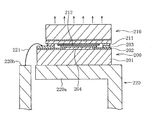
図12に、特許文献1に開示された半導体発光素子及びサブマウント基板の断面図を示す。サブマウント基板200に半導体発光素子210が実装されている。サブマウント基板200は、シリコン基板201の表面上に形成された補助N側電極層203及び補助P側電極層204を含んで構成される。補助N側電極203とシリコン基板201との間に酸化皮膜202が配置され、両者が電気的に絶縁されている。補助P側電極層204は、シリコン基板201の表面上に直接形成されている。補助電極203及び204は、例えば、AuとSnとの合金またはインジウム系の合金で形成される。
FIG. 12 shows a cross-sectional view of the semiconductor light emitting device and the submount substrate disclosed in
サファイア基板を用いた半導体発光素子210の、サブマウント基板200に対向する面上に、N側電極211及びP側電極212が形成されている。N側電極211が補助N側電極層203にハンダ付けされ、P側電極212が補助P側電極層204にハンダ付けされている。
An N-
シリコン基板201がリードフレーム220のP側端子部220aに搭載されている。補助N側電極203が、ワイヤ221により、リードフレーム220のN側端子部220bに接続されている。
A
半導体発光素子210から発光した光は、サファイア基板を通って、サブマウント基板200とは反対側の方向に放射される。
The light emitted from the semiconductor
特許文献2〜4に、半導体発光素子の表面を絶縁性の保護膜で覆う技術が開示されている。特許文献5に、電極と保護膜との間に、Ti、Ni、W等の接着強化層を挿入する技術が開示されている。
図12に示した半導体発光素子210をサブマウント基板(支持基板)200に実装する時に、溶融したAuSn合金等が横にはみ出し、P側電極とN側電極との間が短絡されてしまう場合がある。半導体発光素子を保護膜で覆っても、この短絡を防止することはできない。
When the semiconductor
本発明の目的は、支持基板への実装時における電極の短絡を防止することができる半導体装置及びその製造方法を提供することである。 The objective of this invention is providing the semiconductor device which can prevent the short circuit of the electrode at the time of mounting to a support substrate, and its manufacturing method.
本発明の一観点によると、
第1の面上に第1の電極及び第2の電極が形成されている半導体素子と、
対向面を、前記半導体素子の第1の面に対向させるように配置され、前記第1の電極及び第2の電極にそれぞれ対向する位置に配置された第1の引出電極層及び第2の引出電極層を含む支持基板と、
前記支持基板の対向面及び前記半導体素子の第1の面の少なくとも一方の、少なくとも一部の領域上に配置され、前記第1の電極及び第2の電極に対応する位置にそれぞれ第1の開口及び第2の開口が形成されており、絶縁材料で形成された堰堤膜と、
前記第1の開口内を通って、前記第1の電極と前記第1の引出電極層とを電気的に接続する第1の接続部材と、
前記第2の開口内を通って、前記第2の電極と前記第2の引出電極層とを電気的に接続する第2の接続部材と
を有し、
前記第1の接続部材は、前記第1の電極及び前記第1の引出電極層の一方の上に配置され、前記第1の開口の側面との間に第1の空隙を画定する第1のパッド電極と、他方の上に配置され、前記第1のパッド電極に接続され、前記第1の空隙内に侵入しているが、該第1の空隙を埋め尽くしてはおらず、前記第1のパッド電極と接続する際に溶融及び固化する第1の導電部材とを含み、
前記第2の接続部材は、前記第2の電極及び前記第2の引出電極層の一方の上に配置され、前記第2の開口の側面との間に第2の空隙を画定する第2のパッド電極と、他方の上に配置され、前記第2のパッド電極に接続され、前記第2の空隙内に侵入しているが、該第2の空隙を埋め尽くしてはおらず、前記第2のパッド電極と接続する際に溶融及び固化する第2の導電部材とを含む半導体装置が提供される。
According to one aspect of the invention,
A semiconductor element in which a first electrode and a second electrode are formed on a first surface;
A first extraction electrode layer and a second extraction electrode, which are arranged so as to face the first surface of the semiconductor element, and are arranged at positions facing the first electrode and the second electrode, respectively. A support substrate including an electrode layer;
The first opening is disposed on at least a partial region of at least one of the opposing surface of the support substrate and the first surface of the semiconductor element, and corresponds to the first electrode and the second electrode, respectively. And a second opening is formed, and a dam film formed of an insulating material;
A first connecting member for electrically connecting the first electrode and the first lead electrode layer through the first opening;
A second connecting member for electrically connecting the second electrode and the second extraction electrode layer through the second opening;
The first connection member is disposed on one of the first electrode and the first extraction electrode layer, and defines a first gap between the first connection member and a side surface of the first opening. The pad electrode is disposed on the other side , connected to the first pad electrode, and penetrates into the first gap, but does not fill the first gap, and the first electrode A first conductive member that melts and solidifies when connected to the pad electrode of
The second connection member is disposed on one of the second electrode and the second extraction electrode layer, and defines a second gap between the second connection member and a side surface of the second opening. The pad electrode is disposed on the other , connected to the second pad electrode, and penetrates into the second gap, but does not fill the second gap, and the second electrode And a second conductive member that melts and solidifies when connected to the pad electrode .
本発明の他の観点によると、
第1の面上に第1の電極及び第2の電極が形成されている半導体素子と、
前記半導体素子の第1の面に対向配置され、前記第1の電極及び第2の電極にそれぞれ対向する位置に配置された第1の引出電極層及び第2の引出電極層を含む支持基板と、
前記支持基板の対向面の少なくとも一部の領域上に配置され、前記第1の電極及び第2
の電極に対応する位置にそれぞれ第1の開口及び第2の開口が形成されており、絶縁材料で形成された堰堤膜と、
前記半導体素子の前記第1の面、前記第1の電極、及び前記第2の電極の表面を覆う絶縁材料からなる保護膜であって、該保護膜には、該第1の電極の上面の一部を露出させる第3の開口、及び第2の電極の上面の一部を露出させる第4の開口が形成されており、前記第1の開口を取り囲む環状の領域において、該保護膜の上面が前記堰堤膜の上面に接して、前記第1の開口内の空間と前記第3の開口内の空間とが繋がった第1の空間を形成し、前記第2の開口を取り囲む環状の領域において、該保護膜の上面が前記堰堤膜の上面に接して、前記第2の開口内の空間と前記第4の開口内の空間とが繋がった第2の空間を形成する前記保護膜と、
前記第1の空間内に配置され、前記第1の電極と前記第1の引出電極層とを電気的に接続する第1の接続部材と、
前記第2の空間内に配置され、前記第2の電極と前記第2の引出電極層とを電気的に接続する第2の接続部材と
を有し、
前記第1の接続部材は、前記第1の電極及び前記第1の引出電極層の一方の上に配置され、前記第1の開口の側面との間に第1の空隙を画定する第1のパッド電極と、他方の上に配置され、前記第1のパッド電極に接続され、前記第1の空隙内に侵入しているが、該第1の空隙を埋め尽くしてはおらず、前記第1のパッド電極と接続する際に溶融及び固化する第1の導電部材とを含み、
前記第2の接続部材は、前記第2の電極及び前記第2の引出電極層の一方の上に配置され、前記第2の開口の側面との間に第2の空隙を画定する第2のパッド電極と、他方の上に配置され、前記第2のパッド電極に接続され、前記第2の空隙内に侵入しているが、該第2の空隙を埋め尽くしてはおらず、前記第2のパッド電極と接続する際に溶融及び固化する第2の導電部材とを含む半導体装置が提供される。
According to another aspect of the invention,
A semiconductor element in which a first electrode and a second electrode are formed on a first surface;
A support substrate including a first extraction electrode layer and a second extraction electrode layer disposed opposite to the first surface of the semiconductor element and disposed at positions opposed to the first electrode and the second electrode, respectively; ,
The first electrode and the second electrode are disposed on at least a partial region of the opposing surface of the support substrate.
A first opening and a second opening are respectively formed at positions corresponding to the electrodes, and a dam film formed of an insulating material;
A protective film made of an insulating material covering the surfaces of the first surface, the first electrode, and the second electrode of the semiconductor element, the protective film having an upper surface of the first electrode A third opening exposing a part and a fourth opening exposing a part of the upper surface of the second electrode are formed, and the upper surface of the protective film is formed in an annular region surrounding the first opening. Is in contact with the upper surface of the dam membrane to form a first space in which the space in the first opening and the space in the third opening are connected, and in an annular region surrounding the second opening The protective film forms a second space in which the upper surface of the protective film is in contact with the upper surface of the dam film and the space in the second opening and the space in the fourth opening are connected;
Disposed in the first space, a first connecting member for electrically connecting the first electrode and the first lead electrode layer,
Wherein arranged in the second space, it has a second connection member electrically connects the second electrode and the second lead electrode layer,
The first connection member is disposed on one of the first electrode and the first extraction electrode layer, and defines a first gap between the first connection member and a side surface of the first opening. The pad electrode is disposed on the other, connected to the first pad electrode, and penetrates into the first gap, but does not completely fill the first gap, and the first electrode A first conductive member that melts and solidifies when connected to the pad electrode,
The second connection member is disposed on one of the second electrode and the second extraction electrode layer, and defines a second gap between the second connection member and a side surface of the second opening. The pad electrode is disposed on the other, connected to the second pad electrode, and penetrates into the second gap, but does not fill the second gap, and the second electrode A semiconductor device including a second conductive member that melts and solidifies when connected to a pad electrode is provided.
本発明のさらに他の観点によると、
第1の面上に第1の電極及び第2の電極が形成され、該第1の電極上に第3の接続部材が形成され、該第2の電極上に第4の接続部材が形成されている第1の基板を準備する工程と、
第2の面を、前記第1の基板の第1の面に対向配置した時、該第2の面上の、前記第3の接続部材及び第4の接続部材に対応する位置に、それぞれ第5の接続部材及び第6の接続部材が形成され、該第5の接続部材及び第6の接続部材が、絶縁材料からなる堰堤膜で被覆され、該堰堤膜に、該第5の接続部材及び第6の接続部材の上面を露出させる第1の開口及び第2の開口が形成され、該第1の面の法線に平行な視線で見たとき、該第1の開口の内側に前記第3の接続部材が位置し、該第2の開口の内側に前記第4の接続部材が位置し、前記第1の開口の縁と前記第3の接続部材の縁との間に間隙が画定されており、前記第2の開口の縁と前記第4の接続部材の縁との間に間隙が画定されている第2の基板を準備する工程と、
前記第3の接続部材を、前記第1の開口内を通して前記第5の接続部材に接触させると共に、前記第4の接続部材を、前記第2の開口内を通して前記第6の接続部材に接触させ、該第3の接続部材と第5の接続部材との接触部分、及び前記第4の接続部材と第6の接続部材との接触部分を溶融させ、その後固化させる工程と
を有する半導体装置の製造方法が提供される。
According to yet another aspect of the invention,
A first electrode and a second electrode are formed on the first surface, a third connection member is formed on the first electrode, and a fourth connection member is formed on the second electrode. Preparing a first substrate,
When the second surface is disposed opposite to the first surface of the first substrate, the second surface is positioned at a position corresponding to the third connection member and the fourth connection member, respectively. 5 and 6th connecting members are formed, and the 5th connecting member and the 6th connecting member are covered with a dam film made of an insulating material, and the 5th connecting member and A first opening and a second opening that expose an upper surface of the sixth connection member are formed, and when viewed in a line of sight parallel to a normal line of the first surface, the first opening is formed inside the first opening. 3 connecting members are located, the fourth connecting member is located inside the second opening, and a gap is defined between an edge of the first opening and an edge of the third connecting member. Providing a second substrate having a gap defined between an edge of the second opening and an edge of the fourth connecting member ;
The third connecting member is brought into contact with the fifth connecting member through the first opening, and the fourth connecting member is brought into contact with the sixth connecting member through the second opening. , a semiconductor device having a connecting member and the contact portion of the fifth connecting member of the third, and to melt the contact portion between the fourth connecting member and the sixth connecting member, Ru was then solidifying step A manufacturing method is provided.
本発明のさらに他の観点によると、
第1の面上に第3の接続部材及び第4の接続部材が形成されており、さらに前記第3の接続部材と前記第4の接続部材とを覆い、前記第3の接続部材及び前記第4の接続部材の各々の上面の一部を露出させる絶縁材料からなる保護膜が形成されている第1の基板を準備する工程と、
第2の面上に、絶縁材料からなる堰堤膜が形成され、該第2の面を、前記第1の基板の第1の面に対向配置した時、該堰堤膜の、前記第3の接続部材及び第4の接続部材に対応する位置に、それぞれ第1の開口及び第2の開口が形成され、該第1の開口内及び第2の
開口内にそれぞれ第5の接続部材及び第6の接続部材が配置され、該第5の接続部材と該第1の開口の内周面との間、及び該第6の接続部材と第2の開口の内周面との間に空隙が画定され、該第5の接続部材の上面は第1の開口の開口面から突出し、該第6の接続部材の上面は第2の開口の開口面から突出している第2の基板を準備する工程と、
前記第3の接続部材を前記第5の接続部材に接触させ、前記第4の接続部材を前記第6の接続部材に接触させて、接触部分を溶融させ、その後固化させるとともに、前記第1の開口を取り囲む環状の領域及び前記第2の開口を取り囲む環状の領域において、前記堰堤膜の上面を前記保護膜の上面に接触させる工程と
を有し、
前記第5の接続部材の体積及び前記第1の開口の大きさは、前記溶融させ、その後固化させる工程において、溶融した材料が前記第5の接続部材と前記第1の開口の内周面との間の前記空隙内に侵入し、前記第1の開口の外部には流出しない寸法にされており、前記第6の接続部材の体積及び前記第2の開口の大きさは、前記溶融させ、その後固化させる工程において、溶融した材料が前記第6の接続部材と前記第2の開口の内周面との間の前記空隙内に侵入し、前記第2の開口の外部には流出しない寸法にされている半導体装置の製造方法が提供される。
According to yet another aspect of the invention,
A third connecting member and a fourth connecting member are formed on the first surface, and further covers the third connecting member and the fourth connecting member, and the third connecting member and the fourth connecting member are covered. Preparing a first substrate on which a protective film made of an insulating material exposing a part of the upper surface of each of the four connection members is formed;
A dam film made of an insulating material is formed on the second surface, and the second connection of the dam film when the second surface is disposed opposite to the first surface of the first substrate. A first opening and a second opening are formed at positions corresponding to the member and the fourth connecting member, respectively, and a fifth connecting member and a sixth opening are respectively formed in the first opening and the second opening. A connecting member is disposed, and a gap is defined between the fifth connecting member and the inner peripheral surface of the first opening, and between the sixth connecting member and the inner peripheral surface of the second opening. Preparing a second substrate in which the upper surface of the fifth connecting member protrudes from the opening surface of the first opening, and the upper surface of the sixth connecting member protrudes from the opening surface of the second opening;
The third connecting member is brought into contact with the fifth connecting member, the fourth connecting member is brought into contact with the sixth connecting member, the contact portion is melted and then solidified , and the first connecting member is solidified . Contacting the upper surface of the dam film with the upper surface of the protective film in an annular region surrounding the opening and an annular region surrounding the second opening ;
The volume of the fifth connecting member and the size of the first opening are determined by the molten material in the step of melting and then solidifying the fifth connecting member and the inner peripheral surface of the first opening. The size of the sixth connecting member and the size of the second opening are melted, and the size of the second opening is melted. Thereafter, in the step of solidifying, the melted material enters the gap between the sixth connecting member and the inner peripheral surface of the second opening, and does not flow out of the second opening. A method for manufacturing a semiconductor device is provided.
半導体素子を支持基板に実装する際に、接続部材の一部が溶融する。溶融した金属が、堰堤膜に形成された開口内に止まることにより、電極間の短絡の発生を防止することができる。 When the semiconductor element is mounted on the support substrate, a part of the connection member is melted. Since the molten metal stops in the opening formed in the dam film, it is possible to prevent the occurrence of a short circuit between the electrodes.
図1及び図2を参照して、第1の実施例による半導体装置及びその製造方法について説明する。 With reference to FIG. 1 and FIG. 2, the semiconductor device and the manufacturing method thereof according to the first embodiment will be described.
図1に示すように、第1の実施例による半導体装置は、サブマウント基板1と半導体発光素子30とを含んで構成される。
As shown in FIG. 1, the semiconductor device according to the first embodiment includes a
サブマウント基板1の構造について説明する。シリコン等からなる下地基板2の主面上に、酸化シリコンからなる厚さ300nmの絶縁膜3が形成されている。絶縁膜3の上に、半導体発光素子30のp側電極に接続される引出配線層4及びn側電極に接続される引出配線層5が形成されている。引出配線層4及び5は、例えば厚さ10nmのチタン(Ti)層と厚さ1000nmの金(Au)層との2層構造を有する。なお、引出配線層4及び5を、ニッケル(Ni)層とAu層との2層構造としてもよい。
The structure of the
引出配線層4及び5の上に、それぞれ接着層6及び7が形成されている。接着層6及び7は、例えばTiで形成され、その厚さは10nmである。引出配線層4及び5の上面の一部は、リード線接続のために露出している。
p側の接着層6の一部の表面上に、バリア層8、接続部材10、接着層12がこの順番に積層されている。n側の接着層7の一部の表面上にも、同様にバリア層9、接続部材11、接着層13がこの順番に積層されている。バリア層8及び9は、下地基板2側から順番に厚さ10nmのTi層、厚さ100nmのAu層、及び厚さ100nmの白金(Pt)層が積層された3層構造を有する。接続部材10及び11は、Au層と錫(Sn)層とが交互に配置された積層構造を有する。最下層及び最上層は共にAu層とされている。Au層及びSn層の各々の厚さを、例えば75.5nm及び109.4nmとし、Au層を6層、Sn層を5層配置した。なお、Au層及びSn層の各々の厚さを50nm〜200nmとしてもよい。接着層12はTiで形成され、その厚さは10nmである。
On a part of the surface of the p-side
なお、バリア層8及び9を、タングステン(W)/Au/Ptの3層構造、モリブデン(Mo)/Au/Ptの3層構造としてもよい。ここで、「X/Y/Z」なる表記は、Xが最下層、Yが中層、Zが上層に配置されることを意味する。 The barrier layers 8 and 9 may have a three-layer structure of tungsten (W) / Au / Pt and a three-layer structure of molybdenum (Mo) / Au / Pt. Here, the notation “X / Y / Z” means that X is disposed in the lowermost layer, Y is disposed in the middle layer, and Z is disposed in the upper layer.
p側の接着層6及び12、p側の接続部材10、バリア層8、p側の引出配線層4とn側の引出配線層5との間の絶縁膜3、n側の接着層7及び13、n側の接続部材11、バリア層9が、堰堤膜14で覆われている。堰堤膜14は、例えば酸化シリコンで形成され、その厚さは500nm〜3000nmである。
p-side
堰堤膜14及び接着層12に、p側の接続部材10の上面の一部を露出させる開口15が形成され、堰堤膜14及び接着層13に、n側の接続部材11の上面の一部を露出させる開口16が形成されている。
An
次に、半導体発光素子30の構造について説明する。サファイア基板31の主面上に初期核形成層32、n型半導体層33、活性層34、p型半導体層35がこの順番に積層されている。これらの半導体層は、例えばInyAl1−x−yGaxN(x+y≦1、0≦x≦1、0≦y≦1)等の窒化物半導体で形成される。活性層34及びp型半導体層35の一部が除去され、n型半導体層33の一部が露出している。
Next, the structure of the semiconductor
p型半導体層35の表面上に、p側のオーミック電極36が形成され、n型半導体層33の露出した領域に、n側のオーミック電極37が形成されている。p側のオーミック電極36は、例えば厚さ3nmのPt層と厚さ100nmのロジウム(Rh)層との2層構造を有する。n側のオーミック電極37は、例えば、厚さ3nmのAl層、厚さ100nmのRh層、厚さ100nmのAu層、厚さ100nmのPt層、及び厚さ100nm〜2000nmのAu層が順番に積層された5層構造を有する。サファイア基板31の主面を基準として、p側のオーミック電極36及びn側のオーミック電極37の上面の高さが揃うように、n側のオーミック電極37の最上のAu層の厚さが決定される。
A p-
p側のオーミック電極36を、PtやRhの単層構造にしてもよいし、Pt/銀(Ag)の2層構造にしてもよい。また、n側のオーミック電極37の2層目を、Rhの代わりにPt、イリジウム(Ir)、パラジウム(Pd)等で形成してもよい。
The p-
オーミック電極36及び37の表面上に、それぞれパッド電極(接続部材)38及び39が形成されている。パッド電極38及び39は、例えば厚さ3nmのNi層、厚さ100nmのAu層、厚さ100nmのPt層、及び厚さ200nm〜2000nmのAu層がこの順番に積層された4層構造を有する。パッド電極38及び39の第1層目をNiの代わりにTi、W、またはMoで形成してもよい。また、第2層目のAu層を省略して3層構造としてもよい。パッド電極38及び39の高さは、支持基板1側の開口15及び16の深さ(堰堤膜14の厚さ)に比べてやや大きくなるように設定されている。
Pad electrodes (connection members) 38 and 39 are formed on the surfaces of the
次に、サブマウント基板1の製造方法について説明する。下地基板1を洗浄し、表面を清浄化する。下地基板1の主面上に、酸化シリコンからなる厚さ300nmの絶縁膜3をスパッタリングにより形成する。なお、表面に熱酸化膜が形成されたシリコン基板を用いる場合には、スパッタリングによる絶縁膜形成工程を省略することができる。
Next, a method for manufacturing the
引出配線層4及び5に整合する開口を有するレジストパターンを形成し、引出配線層4及び5となるTi層、Au層、及び接着層6及び7となるTi層を順番に電子ビーム蒸着により形成する。リフトオフ法を用いて、不要な領域のTi層及びAu層を除去し、引出配線層4、5及び接着層6、7を形成する。この時点では、接着層6、7が引出配線層4、5の全面を覆っているが、後のエッチング工程で、引出配線層4、5の表面の一部が露出する。
A resist pattern having openings matching the lead wiring layers 4 and 5 is formed, and a Ti layer to be the lead wiring layers 4 and 5, an Au layer, and a Ti layer to be the adhesion layers 6 and 7 are sequentially formed by electron beam evaporation. To do. The lift-off method is used to remove unnecessary Ti and Au layers, and lead-out wiring layers 4 and 5 and
接続部材10、11に整合する開口を有するレジストパターンを形成し、電子ビーム蒸着により、バリア層8、9から接着層12、13までの各層を堆積する。リフトオフ法により、各層の不要な部分を除去する。これにより、バリア層8、9、接続部材10、11、及び接着層12、13が残る。
A resist pattern having openings matching the
全面に、厚さ500nm〜3000nmの酸化シリコン膜をスパッタリングにより形成する。この酸化シリコン膜をパターニングすることにより、堰堤膜14を残す。このとき、開口15、16が形成され、引出配線層4及び5の表面の一部が露出する。開口15及び16の底面に、接続部材10及び11の最上のAu層が露出する。酸化シリコン膜をウェットエッチングすると、一般的に、開口15及び16の底面が開口面(上面)よりも小さくなるように、その側面が傾斜する。開口15及び16は、その底面が、半導体発光素子30のパッド電極38及び39の最上面よりも大きくなるような形状にされる。
A silicon oxide film having a thickness of 500 nm to 3000 nm is formed on the entire surface by sputtering. By patterning this silicon oxide film, the
シリコン基板2の研削及び研磨を行い、その厚さを100μm程度まで薄くする。スクライブ及びブレーキングを行い、素子単位に分離する。
The
次に、半導体発光素子30の形成方法について説明する。サファイア基板31の主面上に、初期核形成層32、n型半導体層33、活性層34、及びp型半導体層35を成長させる。これらの層は、有機金属気相エピタキシャル成長(MOVPE)、分子線エピタキシャル成長(MBE)により成長させることができる。
Next, a method for forming the semiconductor
p型半導体層35及び活性層34の一部をエッチングして、n型半導体層33の一部を露出させる。このエッチングの深さは、例えば700nmとする。p型半導体層35の表面上に、p側のオーミック電極36を、電子ビーム蒸着とリフトオフ法を用いて形成する。その後、n型半導体層33の露出した領域上に、n側のオーミック電極37を、電子ビーム蒸着とリフトオフ法により形成する。n側のオーミック電極37の最上面の高さが、p側のオーミック電極36の最上面の高さに揃うように、n側のオーミック電極37の最上のAu層の厚さが設定されている。
A part of the p-
オーミック電極36及び37の表面上に、それぞれパッド電極38及び39を、電子ビーム蒸着及びリフトオフ法により形成する。サファイア基板31の研削及び研磨を行い、その厚さを100μm〜230μmまで薄くする。その後、スクライブ及びブレーキングを行い、素子単位に分離する。
次に、半導体発光素子30をサブマウント基板1にフリップチップボンディングする手順を説明する。
Next, a procedure for flip-chip bonding the semiconductor
シリコン基板2の主面とサファイア基板31の主面とが向き合うように、サブマウント基板1と半導体発光素子30とを対向配置させる。シリコン基板2の主面に垂直な視線で見たとき、パッド38が開口15の内側に位置し、パッド39が開口16の内側に位置するように、サブマウント基板1と半導体発光素子30との位置を調整する。
The
パッド電極38及び39を、それぞれ開口15及び16内に挿入し、接続部材10及び11に接触させる。サブマウント基板1と半導体発光素子30とに圧力を印加した状態で加熱して高温状態を保持し、その後冷却する。パッド電極38の最上のAu層と接続部材10とが共晶化され、パッド電極39の最上のAu層と接続部材11が共晶化される。加熱条件として、好適な共晶温度プロファイルが選択される。本実施例で使用したAuSn共晶金属では、Sn濃度が20重量%である。この共晶組成のAuSnの共晶点は280〜300℃である。このように、接続部材10とパッド電極38との接触部分及び接続部材11とパッド電極39との接触部分を共晶化させることにより、半導体発光素子30をサブマウント基板1に固定すると共に、両者の電気的接続を得ることができる。
図2に、半導体発光素子30がサブマウント基板1にボンディングされた状態の半導体装置の断面図を示す。オーミック電極36及び37の上面が、堰堤膜14に形成された開口15及び16を取り囲む環状の領域において、堰堤膜14の上面に接する。このため、オーミック電極36と引出配線層4との間に、堰堤膜14で取り囲まれた閉じた空間が画定される。同様に、オーミック電極37と引出配線層5との間に、堰堤膜14で取り囲まれた閉じた空間が画定される。p側の引出配線層4の露出した領域にリード線40が接続され、n側の引出配線層5の露出した領域にリード線41が接続される。
FIG. 2 is a cross-sectional view of the semiconductor device in a state where the semiconductor
p側のバリア層8、接続部材10、及びパッド電極38が、支持基板1側の引出電極層4と半導体素子30側のオーミック電極36とを電気的に接続する。n側のバリア層9、接続部材11、及びパッド電極39が、支持基板1側の引出電極層5と半導体素子30側のオーミック電極37とを電気的に接続する。
The p-
開口15の内周面とパッド電極38の外周面との間に空隙が画定される。パッド電極38の高さが開口15の深さ(堰堤膜14の厚さ)よりもやや大きいため、パッド電極38の上面側の表層部が接続部材10内に埋め込まれると共に、溶融した金属がこの空隙内に侵入する。実施例においては、パッド電極38の体積が開口15の容積よりも小さくされている。このため、空隙内に溶融した金属が侵入したとしても、空隙を埋め尽くすことはなく、空隙が残存する。従って、溶融した金属が開口15の外に漏れ出すことを防止できる。
A gap is defined between the inner peripheral surface of the
溶融した金属の漏れ出しを防止するためには、パッド電極38の体積を開口15の容積の97%以下にすることが好ましく、95%以下にすることがより好ましい。また、パッド電極38を小さくしすぎると、十分な接着強度が得られない。このため、パッド電極38の体積を開口15の容積の70%以上にすることが好ましく、85%以上にすることがより好ましい。すなわち、開口15の容積に対して、開口15内に残存する空隙の容積の割合を、3%〜30%にすることが好ましく、5%〜15%にすることがより好ましい。
In order to prevent the molten metal from leaking out, the volume of the
n側のパッド39と開口16との関係も、p側のパッド38と開口15との関係と同様である。これにより、p側の電極とn側の電極との短絡故障を防止することができる。
The relationship between the n-
また、堰堤膜14の厚さにより、実装時におけるサブマウント基板1と半導体発光素子30との間隔が規定される。すなわち、接合部材10及び11への、パッド電極38及び39の埋込深さを容易に調整することができる。これにより、パッド電極が必要以上に接合部材中に埋め込まれて溶融した金属が基板面に沿って拡がることを防止できる。
Further, the thickness of the
AuとSnとを共晶化させるときに、接続部材10及び11が溶融した状態では、サブマウント基板1と半導体発光素子30との相対位置が不安定になる。第1の実施例では、半導体発光素子30のパッド電極38及び39が、それぞれサブマウント基板1の開口15及び16内に挿入されているため、接続部材10及び11が溶融した状態でも、サブマウント基板1と半導体発光素子30との相対位置を拘束することができる。これにより、位置ずれに起因する歩留まりの低下を防止することができる。十分な位置ずれ防止効果を得るために、堰堤膜14の厚さを500nm以上とすることが好ましい。酸化シリコンのエッチング工程における処理時間やサイドエッチングの深さ等の観点から、堰堤膜14の厚さを3000nm以下とすることが好ましく、1000nm以下とすることがより好ましい。
When Au and Sn are eutectic, the relative position between the
パッド電極38の最上のAu層と接続部材10とで形成されたAuSn共晶部材が、堰堤膜14により画定された閉じた空間内に配置される。このため、AuSn共晶部材が配置された空間への水分の侵入を防止することができる。一般に、水分の存在下でSnが電気化学的マイグレーションを起こしやすいことが知られている。第1の実施例では、AuSn共晶部材が水分に晒されることを抑制できるため、Snのマイグレーションを抑制し、半導体装置の信頼性向上を図ることができる。
An AuSn eutectic member formed by the uppermost Au layer of the
第1の実施例では、1層の厚さを50nm〜200nmとしたAuとSnとの多層構造を加熱することによりAuSn共晶部材を形成した。これにより、一般的なAuSn共晶合金法に比べて、安定した共晶過程を得ることができた。例えば、Snの含有量が20重量%のAuSn合金を蒸着源として用いた場合、AuとSnとの蒸発量が経時的に変化する。このため、堆積膜の組成が目標とする組成からずれてしまう。組成がずれると共晶温度が変化してしまい、共晶反応が不十分になる場合がある。多層構造にすることにより、接続部材の組成を目標値に近づけ、共晶反応を安定化させることができる。 In the first example, an AuSn eutectic member was formed by heating a multilayer structure of Au and Sn having a thickness of one layer of 50 nm to 200 nm. Thereby, a stable eutectic process could be obtained as compared with a general AuSn eutectic alloy method. For example, when an AuSn alloy having a Sn content of 20% by weight is used as a deposition source, the evaporation amount of Au and Sn changes with time. For this reason, the composition of the deposited film deviates from the target composition. If the composition shifts, the eutectic temperature changes, and the eutectic reaction may become insufficient. By adopting a multilayer structure, the composition of the connecting member can be brought close to the target value and the eutectic reaction can be stabilized.
次に、接続部材10、11の積層構造、及びそれに対向するパッド電極38、39の最上のAu層の厚さについて説明する。AuとSnとの共晶合金の共晶比を、重量比でAu:Sn=80:20とする場合を考える。この場合、AuとSnとの体積比は0.544:0.456になる。ここで、スパッタリングで成膜したSn膜は灰色錫であることがわかったため、その密度を5.76g/cm3とした。以下の説明では、一般化して、共晶金属全体に対するAu及びSnの体積比を、それぞれVau及びVsnとする。
Next, the laminated structure of the
接続部材10を構成するSn層の層数をnとすると、Au層の層数はn+1になる。さらにパッド電極38の最上のAu層も共晶反応に関与するため、共晶反応に関与するAu層の層数はn+2になる。
When the number of Sn layers constituting the connecting
パッド電極38の最上のAu層と接続部材10との合計の厚さをLtとする。このとき、各Au層の厚さLau、各Sn層の厚さLsnは、
The total thickness of the uppermost Au layer of the
(数1)
Lau=Lt×Vau/(n+2)
Lsn=Lt×Vsn/n
となる。合計の厚さLtを1200nm、Sn層の層数nを5とすると、Vau=0.544、Vsn=0.456のとき、
(Equation 1)
Lau = Lt × Vau / (n + 2)
Lsn = Lt × Vsn / n
It becomes. Assuming that the total thickness Lt is 1200 nm and the number of Sn layers n is 5, when Vau = 0.544 and Vsn = 0.456,
(数2)
Lau=93.3nm
Lsn=109.4nm
となる。
(Equation 2)
Lau = 93.3 nm
Lsn = 109.4 nm
It becomes.
上記第1の実施例において、堰堤膜14の厚さを1000nmとし、パッド電極38を構成するNi/Au/Pt/Au層の厚さを、それぞれ3nm/100nm/100nm/1000nmとした場合について考察する。この場合、パッド電極38の上面の厚さ約200nmの表層部が、接続部材14内に埋め込まれる。この厚さ200nmの表層部が共晶反応に関与すると考えることができる。共晶金属部全体の厚さLtを1200nmとすると、Au層の全体の厚さは1200×Vau[nm]になる。このうちの200nmの部分がパッド電極38から供給されるため、接続部材10を構成するAu層の全体の厚さを(1200×Vau−200)[nm]にすればよい。Au層の層数が6であるから、各Au層の厚さは75.5nmになる。また、各Sn層の厚さは、上述の計算結果どおり、109.4nmになる。
In the first embodiment, the thickness of the
このように、接続部材10を構成するSn層の体積比が、共晶比から求められる体積比よりも大きくされている。従って、接続部材10が溶融した時に、Snに比べてAuが不足する。不足したAuを補うために、パッド電極38の最上のAu層が溶融して共晶反応が生ずることになる。このようにして、パッド電極38と接続部材10との接着性を高めることができる。
Thus, the volume ratio of the Sn layer constituting the
また、第1の実施例では、引出配線層4と堰堤膜14との間に接着層6が配置され、引出配線層5と堰堤膜14との間に接着層7が配置されている。接続部材10の上面(半導体発光素子30に対向する面)は、パッド電極38の上面(支持基板1に対向する面)よりも広い。堰堤膜14は、接続部材10の上面の一部に、接着層12を介して密着する。接続部材11とパッド電極39との関係も同様であり、堰堤膜14が接着層13を介して接続部材11の上面の一部に密着する。接着層12は、堰堤膜14の密着性を高める機能を有する。実施例では、接着層の材料としてTiを用いたが、NiやAlを用いてもよい。
In the first embodiment, the
活性層34に電流を注入すると、発光が生ずる。サファイア基板31は、この光を透過させる。このため、サファイア基板31を通して、光が外部に放射される。サブマウント基板1の方に向かって伝搬する光は、p側のオーミック電極36で反射され、サファイア基板31を通して外部に放射される。
When current is injected into the
上記第1の実施例では、サブマウント基板1の下地として導電性を有するシリコン基板を用いたが、窒化アルミニウム(AlN)やアルミナ(Al2O3)等の絶縁性の基板を用いてもよい。この場合には、図1に示した絶縁膜3を形成することなく、下地基板の上に引出配線層4及び5を直接形成してもよい。下地基板の材料として、熱伝導率が高く、かつ熱膨張係数が半導体発光素子の熱膨張係数と近いものが好ましい。このような導電性材料の例として、シリコン以外にCuW等が挙げられる。
In the first embodiment, a conductive silicon substrate is used as the base of the
上記実施例では、堰堤膜14の材料として酸化シリコンを用いたが、その他の絶縁材料を用いてもよい。例えば、アルミナ(Al2O3)、酸化チタン(TiO2、Ti2O5)、ジルコニア(ZrO2)、ハフニア(HfO2)等の耐熱性の酸化物絶縁材料、またはポリイミド樹脂等の耐熱性高分子材料を用いてもよい。
In the above embodiment, silicon oxide is used as the material for the
次に、図3及び図4を参照して、第2の実施例について説明する。図3にフリップチップボンディング前の状態を示し、図4に、フリップチップボンディング後の状態を示す。第2の実施例による半導体装置と第1の実施例による半導体装置との主な相違点は、第2の実施例では、半導体発光素子30の、サブマウント基板1に対向する面が保護膜50で覆われている点である。第1の実施例では、保護膜は形成されていなかった。以下、第1の実施例との相違点について説明する。
Next, a second embodiment will be described with reference to FIGS. FIG. 3 shows a state before flip chip bonding, and FIG. 4 shows a state after flip chip bonding. The main difference between the semiconductor device according to the second embodiment and the semiconductor device according to the first embodiment is that, in the second embodiment, the surface of the semiconductor
図3に示すように、半導体発光素子30の、サブマウント基板1に対向する面が、酸化シリコンからなる保護膜50で覆われている。サブマウント基板1の開口15及び16に対応する位置に、それぞれ保護膜50を貫通する開口53及び54が形成されている。開口53及び54の底面に、それぞれオーミック電極36及び37の上面が現われている。開口53の底面に現われたオーミック電極36の表面上にパッド電極38が形成され、開口54の底面に現われたオーミック電極37の表面上にパッド電極39が形成されている。
As shown in FIG. 3, the surface of the semiconductor
p側のオーミック電極36の上面と保護膜50との間に接着層51が配置され、n側のオーミック電極37の上面と保護膜50との間に接着層52が配置されている。接着層51及び52は、Ti、Ni、Al等で形成される。
An
以下、半導体発光素子30の製造方法について、第1の実施例による半導体発光素子30との相違点に着目して説明する。
Hereinafter, a method for manufacturing the semiconductor
p側のオーミック電極36を形成するときに、Pt層とRh層との2層のみではなく、Rh層の上にさらに厚さ10nmのTi層を電子ビーム蒸着する。リフトオフ法により、オーミック電極36を形成する。この時点で、オーミック電極36の上面に、接着層51となるTi層が残っている。n側のオーミック電極37を形成するときに、Al/Rh/Au/Pt/Auの5層のみではなく、さらに厚さ10nmのTi層を電子ビーム蒸着する。リフトオフ法により、オーミック電極37を形成する。この時点で、オーミック電極37の上面に、接着層52となるTi層が残っている。
When forming the p-
全面を覆うように、酸化シリコンからなる厚さ300nmの保護膜50を、スパッタリングにより形成する。保護膜50の一部をレジストパターンで覆ってエッチングすることにより、開口53及び54を形成する。このとき、開口53及び54の底面に露出するTi層もエッチングされ、オーミック電極36及び37の上面が露出する。
A
パッド電極38及び39を、電子ビーム蒸着とリフトオフ法により形成する。パッド電極38及び39は、厚さ3nmのNi層、厚さ100nmのAu層、厚さ100nmのPt層、及び厚さ200nm〜2000nmのAu層がこの順番に積層された4層構造を有する。最上のAu層の厚さは、サブマウント基板1側の開口15及び16の深さ(堰堤膜14の厚さ)、パッド電極38及び39の表面の平坦度、適当な押し当て代等を加味して決定される。堰堤膜14の厚さが1μm、保護膜50の厚さが300nm、パッド電極38及び39の表面のうねりが20nmであり、押し当て代を200nmとすると、パッド電極38及び39の最上のAu層の好適な厚さは、一例として1300nmになる。すなわち、第1の実施例のパッド電極38及び39の厚さよりも、保護膜50の厚さ分だけ厚くされている。
図4に示すように、半導体発光素子30をサブマウント基板1に実装した状態では、保護膜50の上面が、開口15及び16の周囲(開口15及び16の各々を取り囲む環状の領域)において堰堤膜14の上面に接する。p側のオーミック電極36と引出配線層4との間、及びn側のオーミック電極37と引出配線層5との間に、堰堤膜14と保護膜50で取り囲まれた閉じた空間が画定される。
As shown in FIG. 4, when the semiconductor
サブマウント基板1側に形成された開口15の容積を、パッド電極38のうち保護膜50の上面から突出した部分の体積よりも大きくしておくことにより、溶融した金属が開口15の外部に流出することを防止できる。同様に、開口16の容積を、パッド電極39のうち保護膜50の上面から突出した部分の体積よりも大きくしておくことにより、溶融した金属が開口16の外部に流出することを防止できる。
By making the volume of the
なお、第2の実施例の場合には、半導体発光素子30側にも開口53及び54が設けられているため、これらの開口をも考慮して、パッド電極38及び39の体積を設定してもよい。例えば、パッド電極38の体積を、開口15の容積と開口53の容積との和よりも小さくしておけばよい。第1の実施例の場合と同様に、パッド電極38の体積を、開口15の容積と開口53の容積との和の97%以下とすることが好ましく、95%以下とすることがより好ましい。また、パッド電極38の体積を、開口15の容積と開口53の容積との和の70%以上とすることが好ましく、85%以上とすることがより好ましい。
In the case of the second embodiment, since the
第1の実施例では、図2に示したように、オーミック電極36及び37の一部が露出する。これに対し、第2の実施例では、図4に示したように、オーミック電極36及び37が保護膜50で完全に覆われる。サブマウント基板1と半導体発光素子30との接続に関与する金属部材が露出しないため、耐候性の向上を図ることができる。
In the first embodiment, as shown in FIG. 2, the
図5を参照して、第3の実施例による半導体装置について説明する。図5は、半導体発光素子30aをサブマウント基板1aに実装する前の状態の断面図である。
A semiconductor device according to the third embodiment will be described with reference to FIG. FIG. 5 is a cross-sectional view of a state before the semiconductor
サブマウント基板1aの構造及び製造方法について説明する。第1の実施例の場合と同様に、シリコン基板2の主面上に、絶縁膜3、引出配線層4、5、及び接着層6、7が形成されている。
The structure and manufacturing method of the submount substrate 1a will be described. As in the case of the first embodiment, an insulating
接着層6の表面の一部の領域上にp側のパッド電極(サブマウント基板側の接続部材)61が形成され、その上に接着層63が形成されている。接着層5の表面の一部の領域上にn側のパッド電極62が形成され、その上に接着層64が形成されている。パッド電極61及び62は、厚さ10nmのTi層、厚さ100nmのAu層、厚さ100nmのPt層、及び厚さ600nmのAu層がこの順番で積層された4層構造を有する。接着層63及び64は、厚さ10nmのTi層で構成される。これらの層は、引出配線層4、5及び接着層6、7を形成した後、電子ビーム蒸着とリフトオフ法により形成される。本実施例においては、パッド電極61及び62の最上のAu層の厚さを100nm〜1000nmとしてもよい。
A p-side pad electrode (submount substrate-side connecting member) 61 is formed on a partial region of the surface of the
厚さ1000nmの酸化シリコン膜を全面に堆積し、パターニングすることにより、堰堤膜14aが形成されている。このパターニング時に、接着層6、7、63、及び64の露出した部分がエッチングされる。堰堤膜14aには、パッド電極61及び62の上面を露出させる開口15a及び16aが形成されるとともに、引出配線層4及び5の一部が露出する。
A
次に、半導体発光素子30aの構造及び製造方法について説明する。図1に示した第1の実施例の場合と同様に、サファイア基板31の主面上に、初期核形成層32、n型半導体層33、活性層34、p型半導体層35、p側のオーミック電極36、及びn側のオーミック電極37が形成されている。ただし、n側のオーミック電極37は、第1の実施例のn側のオーミック電極37よりも薄く、厚さ3nmのAl層と厚さ100nmのRh層との2層構造を有する。
Next, the structure and manufacturing method of the semiconductor
p側のオーミック電極36の表面上にバリア層71が形成され、n側のオーミック電極37の表面上にバリア層72が形成されている。バリア層71は、厚さ100nmのAu層、厚さ100nmのPt層、及び厚さ100nmのAu層がこの順番に積層された3層構造を有する。バリア層72は、厚さ100nmのAu層、厚さ100nmのPt層、及び厚さ800nmのAu層がこの順番に積層された3層構造を有する。なお、最上のAu層の厚さは、必要に応じて100nm〜2000nmの範囲内から選択される。なお、n側のオーミック電極37とバリア層72との全体は、Al/Rh/Au/Pt/Auの5層構造を有し、図1に示した第1の実施例のn側オーミック電極37と同一の積層構造になる。第3の実施例では、基板側のAl/Rhの2層をオーミック電極と呼び、その上のAu/Pt/Auの3層をバリア層と呼ぶこととする。
A
バリア層71の表面の一部の領域上に、p側の接続部材73が形成され、バリア層72の表面の一部の領域上に、n側の接続部材74が形成されている。接続部材73及び74は、厚さ20nmのNi層と、その上にAu層とSn層とが交互に配置された多層構造を有する。第3の実施例では、Au層の厚さを80.3nmとし、Sn層の厚さを106.3nmとした。また、Au層を7層、Sn層を6層配置することにより、最下層及び最上層を共にAu層とした。
A p-
サブマウント基板1aと半導体発光素子30aとを対向配置した状態で、基板の主面の法線に平行な視線で見たとき、接続部材73が開口15aに内包され、接続部材74が開口16aに内包される。バリア層71は開口15aの外周よりも外側まで広がり、バリア層72は開口16aの外周よりも外側まで広がる。
When the submount substrate 1a and the semiconductor
次に、半導体発光素子30aの製造方法について説明する。活性層34及びp型半導体層35の一部をエッチングして、n型半導体層33の一部を露出させる工程までは、第1の実施例の場合と同様である。
Next, a method for manufacturing the semiconductor
p型半導体層35の表面上に、電子ビーム蒸着とリフトオフ法により、オーミック電極36及びバリア層71を形成する。その後、n型半導体層33の表面の露出した領域上に、電子ビーム蒸着とリフトオフ法により、オーミック電極37及びバリア層72を形成する。次に、電子ビーム蒸着とリフトオフ法により、バリア層71及び72の上に、それぞれ接続部材73及び74を形成する。
An
接続部材73及び74を、それぞれ開口15a及び16a内に挿入し、接続部材73、74、及びパッド電極61、62の最上のAu層を共晶化させる。バリア層71及び72の上面の一部が、それぞれ開口15a及び16aの周囲において堰堤膜14aの上面に接する。これにより、バリア層71と引出配線層4との間、及びバリア層72と引出配線層5との間に、堰堤膜14aで囲まれた閉じた空間が画定される。接続部材73とパッド電極61、及び接続部材74とパッド電極62は、これらの閉じた空間内に配置される。このため、第1の実施例の場合と同様に、溶融した金属が開口15a及び16aから外部に漏れ出すことを防止できる。
The connecting
図6に示すように、半導体発光素子30aの、サブマウント基板1aに対向する面を、図3に示した第2の実施例の場合と同様に、酸化シリコンからなる保護膜75で覆ってもよい。保護膜75とバリア層71の上面との間に接着層76が配置され、保護膜75とバリア層72の上面との間に接着層77が配置されている。半導体発光素子30aをサブマウント基板1aに実装した状態では、保護膜75の上面が、開口15a及び16aの周囲において堰堤膜14aの上面に接する。接続部材73及び74は、図5に示した接続部材73及び74よりも、接着層76と保護膜75との合計の厚さ分だけ厚くされる。
As shown in FIG. 6, the surface of the semiconductor
図7を参照して、第4の実施例による半導体装置について説明する。以下、図5に示した第3の実施例による半導体装置と対比しながら説明する。 A semiconductor device according to the fourth embodiment will be described with reference to FIG. Hereinafter, description will be made in comparison with the semiconductor device according to the third embodiment shown in FIG.
第4の実施例のサブマウント基板1bにおいては、第3の実施例のパッド電極61及び62の代わりに、バリア層81及び82が配置されている。バリア層81及び82の構造は、パッド電極61及び62の構造と同一である。開口15aの底面に露出したバリア層81の上に、接続部材83が形成され、開口16aの底面に露出したバリア層82の上に、接続部材84が形成されている。その他の構成は、第3の実施例によるサブマウント基板1aの構成と同様である。接続部材83と開口15aの内周面との間に空隙が画定され、接続部材84と開口16aの内周面との間にも空隙が画定されている。接続部材83及び84の上部は、堰堤膜14aの上面からやや突出している。接続部材83の体積は、開口15aの容積よりも小さく、接続部材84の体積は、開口16aの容積よりも小さい。
In the
接続部材83及び84は、開口15a及び16aを有する堰堤膜14aを形成した後、電子ビーム蒸着とリフトオフ法により形成される。
The
第4の実施例における半導体発光素子30bにおいては、第3の実施例のバリア層71及び72の代わりに、パッド電極87及び88が配置されている。パッド電極87及び88の構造は、バリア層71及び72の構造と同一である。第4の実施例では、サブマウント基板1b上に接続部材83及び84が配置されているため、半導体発光素子30bには、第3の実施例の接続部材73及び74に相当する部材は配置されていない。
In the semiconductor
半導体発光素子30bをサブマウント基板1bに実装した状態では、パッド電極87及び88の上面が、開口15a及び16aの周囲において、堰堤膜14aの上面に接触する。接続部材83、84、及びパッド電極87、88の最上のAu層が共晶化する。溶融した金属は、開口15a及び16a内の空隙内に侵入し、開口15a及び16aの外部には流出しない。
In a state where the semiconductor
第1の実施例の場合と同様に、接続部材83の体積を、開口15aの容積の97%以下にすることが好ましく、95%以下にすることがより好ましい。また、接続部材83の体積を、開口15aの容積の70%以上にすることが好ましく、85%以上にすることがより好ましい。
As in the case of the first embodiment, the volume of the connecting
図8に示すように、半導体発光素子30bの、サブマウント基板1bに対向する面を、酸化シリコンからなる保護膜90で覆ってもよい。保護膜90とパッド電極87の上面との間に接着層91が配置され、保護膜90とパッド電極88の上面との間に接着層92が配置されている。サブマウント基板1bの開口15a及び16aに対応する位置に、保護膜90及び接着層91、92を貫通し、パッド電極87及び88の一部を露出させる開口93及び94が形成されている。
As shown in FIG. 8, the surface of the semiconductor
サブマウント基板1bの接続部材83及び84は、図7に示した接続部材83及び84よりも、保護膜90と接着層91との合計の厚さ分だけ厚くされている。接続部材83及び84が、それぞれ開口93及び94の底面に露出したパッド電極87及び88に密着して共晶化が行われる。
The
図9(A)及び図9(B)を参照して、第5の実施例による半導体装置について説明する。図9(A)に、半導体発光素子30cの断面図を示し、図9(B)に、その底面図を示す。図9(B)の一点鎖線A9−A9における断面図が図9(A)に相当する。図1に示した第1の実施例の半導体発光素子30と対比しながら説明する。
With reference to FIGS. 9A and 9B, a semiconductor device according to a fifth embodiment will be described. FIG. 9A shows a cross-sectional view of the semiconductor
第1の実施例においては、パッド電極38が一つの部分で構成されていたが、第5の実施例では、パッド電極38に対応する部材が4つの部分38a〜38dに分割されている。さらに、パッド電極39に対応する部分が2つの部分39a及び39bに分割されている。その他の構成は、図1に示した第1の実施例の半導体発光素子30と同一である。
In the first embodiment, the
パッド電極の各部分38a〜38dの相互に隣り合う部分の間に間隙が画定されている。また、パッド電極の2つの部分39aと39bとの間にも間隙が画定されている。
A gap is defined between adjacent portions of the
パッド電極が大きくなると、共晶接着工程において、パッド電極を図1に示す接合部材10及び11に押し付け、接続部材10、11及びパッド電極の一部を溶融させた際に、溶融した金属が偏流を起こし、堰堤膜14を乗り越えて、開口15及び16の外部に流出してしまう場合がある。第5の実施例のように、パッド電極を複数の部分に分割し、相互に隣り合う部分の間に間隙を設けておくと、溶融した金属がこの間隙内に侵入する。このため、溶融した金属の偏流を防止でき、安定した接着が可能になる。
When the pad electrode is enlarged, in the eutectic bonding process, the molten metal drifts when the pad electrode is pressed against the
パッド電極の分割は、第1の実施例による半導体発光素子のパッド電極に限らず、その他の実施例によるパッド電極に適用してもよいし、接続部材を分割してもよい。例えば、図5に示した第3の実施例に適用する場合には、半導体発光素子30a上に配置された接続部材73及び74の各々を複数の部分に分割すればよい。図7に示した第4の実施例に適用する場合には、開口15a及び16a内に配置された接続部材83及び84の各々を複数の部分に分割すればよい。また、パッド電極や接続部材を完全に分離してしまう必要はなく、パッド電極の上面(接続部材に対向する面)や接続部材の上面(パッド電極に対向する面)に溝を形成してもよい。半導体基板をサブマウント基板に実装した状態では、接続部材を形成する材料(AuSn共晶金属)がこの溝内に侵入している。図9(A)に示した例は、この溝の深さがパッド電極38a〜38d及び39a、39bの厚さと等しい特殊な場合と考えることができる。
The division of the pad electrode is not limited to the pad electrode of the semiconductor light emitting device according to the first embodiment, but may be applied to the pad electrode according to other embodiments, or the connection member may be divided. For example, when applied to the third embodiment shown in FIG. 5, each of the
図10を参照して、第6の実施例による半導体装置について説明する。第1〜第5の実施例では、堰堤膜がサブマウント基板側に配置されていたが、第6の実施例では、半導体発光素子側に配置されている。 A semiconductor device according to the sixth embodiment will be described with reference to FIG. In the first to fifth embodiments, the dam film is arranged on the submount substrate side, but in the sixth embodiment, it is arranged on the semiconductor light emitting element side.
サブマウント基板1dの構造について説明する。シリコン基板1、絶縁膜3、引出配線層4及び5は、図1に示した第1の実施例の場合と同様である。p側の引出配線層4の表面の一部の領域上にパッド電極101が形成され、n側の引出配線層5の表面の一部の領域上にパッド電極102が形成されている。パッド電極101及び102は、基板側から順番にNi/Au/Pt/Auが積層された4層構造を有する。
The structure of the
半導体発光素子30dの構造について説明する。サファイア基板31、初期核形成層32、n型半導体層33、活性層34、p型半導体層35、オーミック電極36、37、及びバリア層71、72は、図5に示した半導体発光素子30aと同様の構造である。バリア層71の上に接続部材73aが形成され、バリア層72の上に接続部材74aが形成されている。接続部材73aの上面に接着層104が形成され、接続部材74aの上面に接着層105が形成されている。オーミック電極36から接着層104までの積層構造が、電子ビーム蒸着とリフトオフ法を利用した工程で形成される。オーミック電極37から接着層105までの積層構造が、電子ビーム蒸着とリフトオフ法を利用した他の工程で形成される。
The structure of the semiconductor
半導体発光素子30dの、サブマウント基板1dに対向する面が、酸化シリコンからなる堰堤膜103で覆われている。堰堤膜103及び接着層104に開口106が形成され、その底面に接続部材73aが露出している。堰堤膜103及び接着層105に開口107が形成され、その底面に接続部材74aが露出している。
A surface of the semiconductor
サブマウント基板1dと半導体発光素子30dとを対向させた状態で、基板法線に平行な視線で見たとき、パッド電極101が開口106に内包され、パッド電極102が開口107に内包される。パッド電極101を開口106内に挿入して接続部材73aに接触させ、パッド電極102を開口107内に挿入して接続部材74aに接触させる。パッド電極101の最上のAu層と接続部材73a、及びパッド電極102の最上のAu層と接続部材74aとを共晶化させることにより、半導体発光素子30dがサブマウント基板1dに実装される。
The
パッド電極101の体積を開口106の容積よりも小さくし、パッド電極102の体積を開口107の容積よりも小さくしておくことにより、共晶化時に溶融した金属が開口106及び107の外部に漏れ出すことを防止できる。
By making the volume of the
図11を参照して第7の実施例による半導体装置について、図1に示した第1の実施例による半導体装置と対比しながら説明する。第7の実施例による半導体発光素子30eは、第1の実施例による半導体発光素子30と同様の構造を有する。
A semiconductor device according to the seventh embodiment will be described with reference to FIG. 11 in comparison with the semiconductor device according to the first embodiment shown in FIG. The semiconductor
第1の実施例では、シリコン基板2上に形成された絶縁膜3の表面上に、p側の引出配線層4とn側の引出配線層5とが形成されていたが、第7の実施例では、p側の引出配線層4eが、n側の接続部材の配置されている領域まで延在している。p側の引出配線層4eの表面の一部の領域上に、バリア層8e、接続部材10e、及び接着層12eがこの順番に積層されている。各層の構造は、図1に示した第1の実施例のバリア層8、接続部材10、及び接着層12と同様である。
In the first embodiment, the p-side lead wiring layer 4 and the n-side lead wiring layer 5 are formed on the surface of the insulating
p側の引出配線層4eの他の領域上に、接着層111及び絶縁膜112を介して、n側の引出配線層5e、接着層7e、バリア層9e、接続部材11e、及び接着層13eがこの順番に積層されている。接着層111は例えばTiで形成され、絶縁膜112は例えば酸化シリコンで形成されている。引出配線層5eから接着層13eまでの積層構造は、図1に示した第1の実施例のn側の引出配線層5から接着層13までの積層構造と同様である。接続部材10eと13eとの上面の高さが揃うように、バリア層または接続部材の厚さが調節されている。
The n-side lead-out
サブマウント基板1eの、半導体発光素子30eに対向する面上に堰堤膜14eが形成されている。堰堤膜14eと接着層12eとに開口15eが形成され、その底面に接続部材10eが露出している。堰堤膜14eと接着層13eに開口16eが形成され、その底面に接続部材11eが露出している。
A
第7の実施例では、n側の引出配線層5eとp側の引出配線層4eとにより、絶縁膜112を誘電体層とするキャパシタが構成される。これにより、静電破壊耐圧の向上を図ることができる。また、サブマウント基板の下地のシリコン基板に、予めツェナーダイオードやバリスタを形成しておいてもよい。これらの素子は、静電破壊防止に有効である。
In the seventh embodiment, the n-side
以上実施例に沿って本発明を説明したが、本発明はこれらに制限されるものではない。例えば、種々の変更、改良、組み合わせ等が可能なことは当業者に自明であろう。 Although the present invention has been described with reference to the embodiments, the present invention is not limited thereto. It will be apparent to those skilled in the art that various modifications, improvements, combinations, and the like can be made.
1 サブマウント基板
2 シリコン基板
3、112 絶縁膜
4、5 引出配線層
6、7、12、13、51、52、76、77、91、92、104、105、111 接着層
8、9、71、72、81、82 バリア層
10、11、73、74、83、84 接続部材
14、103 堰堤膜
15、16、53、54、93、94、106、107 開口
30 半導体発光素子
31 サファイア基板
32 初期核成長層
33 n型半導体層
34 活性層
35 p型半導体層
36、37 オーミック電極
38、39、61、62、87、88、101、102 パッド電極(接続部材)
40、41 リード線
50、75、90 保護膜
1
40, 41
Claims (6)
対向面を、前記半導体素子の第1の面に対向させるように配置され、前記第1の電極及び第2の電極にそれぞれ対向する位置に配置された第1の引出電極層及び第2の引出電極層を含む支持基板と、
前記支持基板の対向面及び前記半導体素子の第1の面の少なくとも一方の、少なくとも一部の領域上に配置され、前記第1の電極及び第2の電極に対応する位置にそれぞれ第1の開口及び第2の開口が形成されており、絶縁材料で形成された堰堤膜と、
前記第1の開口内を通って、前記第1の電極と前記第1の引出電極層とを電気的に接続する第1の接続部材と、
前記第2の開口内を通って、前記第2の電極と前記第2の引出電極層とを電気的に接続する第2の接続部材と
を有し、
前記第1の接続部材は、前記第1の電極及び前記第1の引出電極層の一方の上に配置され、前記第1の開口の側面との間に第1の空隙を画定する第1のパッド電極と、他方の上に配置され、前記第1のパッド電極に接続され、前記第1の空隙内に侵入しているが、該第1の空隙を埋め尽くしてはおらず、前記第1のパッド電極と接続する際に溶融及び固化する第1の導電部材とを含み、
前記第2の接続部材は、前記第2の電極及び前記第2の引出電極層の一方の上に配置され、前記第2の開口の側面との間に第2の空隙を画定する第2のパッド電極と、他方の上に配置され、前記第2のパッド電極に接続され、前記第2の空隙内に侵入しているが、該第2の空隙を埋め尽くしてはおらず、前記第2のパッド電極と接続する際に溶融及び固化する第2の導電部材とを含む半導体装置。 A semiconductor element in which a first electrode and a second electrode are formed on a first surface;
A first extraction electrode layer and a second extraction electrode, which are arranged so as to face the first surface of the semiconductor element, and are arranged at positions facing the first electrode and the second electrode, respectively. A support substrate including an electrode layer;
The first opening is disposed on at least a partial region of at least one of the opposing surface of the support substrate and the first surface of the semiconductor element, and corresponds to the first electrode and the second electrode, respectively. And a second opening is formed, and a dam film formed of an insulating material;
A first connecting member for electrically connecting the first electrode and the first lead electrode layer through the first opening;
A second connecting member for electrically connecting the second electrode and the second extraction electrode layer through the second opening;
The first connection member is disposed on one of the first electrode and the first extraction electrode layer, and defines a first gap between the first connection member and a side surface of the first opening. The pad electrode is disposed on the other side , connected to the first pad electrode, and penetrates into the first gap, but does not fill the first gap, and the first electrode A first conductive member that melts and solidifies when connected to the pad electrode of
The second connection member is disposed on one of the second electrode and the second extraction electrode layer, and defines a second gap between the second connection member and a side surface of the second opening. The pad electrode is disposed on the other , connected to the second pad electrode, and penetrates into the second gap, but does not fill the second gap, and the second electrode And a second conductive member that melts and solidifies when connected to the pad electrode .
前記半導体素子の第1の面に対向配置され、前記第1の電極及び第2の電極にそれぞれ対向する位置に配置された第1の引出電極層及び第2の引出電極層を含む支持基板と、
前記支持基板の対向面の少なくとも一部の領域上に配置され、前記第1の電極及び第2
の電極に対応する位置にそれぞれ第1の開口及び第2の開口が形成されており、絶縁材料で形成された堰堤膜と、
前記半導体素子の前記第1の面、前記第1の電極、及び前記第2の電極の表面を覆う絶縁材料からなる保護膜であって、該保護膜には、該第1の電極の上面の一部を露出させる第3の開口、及び第2の電極の上面の一部を露出させる第4の開口が形成されており、前記第1の開口を取り囲む環状の領域において、該保護膜の上面が前記堰堤膜の上面に接して、前記第1の開口内の空間と前記第3の開口内の空間とが繋がった第1の空間を形成し、前記第2の開口を取り囲む環状の領域において、該保護膜の上面が前記堰堤膜の上面に接して、前記第2の開口内の空間と前記第4の開口内の空間とが繋がった第2の空間を形成する前記保護膜と、
前記第1の空間内に配置され、前記第1の電極と前記第1の引出電極層とを電気的に接続する第1の接続部材と、
前記第2の空間内に配置され、前記第2の電極と前記第2の引出電極層とを電気的に接続する第2の接続部材と
を有し、
前記第1の接続部材は、前記第1の電極及び前記第1の引出電極層の一方の上に配置され、前記第1の開口の側面との間に第1の空隙を画定する第1のパッド電極と、他方の上に配置され、前記第1のパッド電極に接続され、前記第1の空隙内に侵入しているが、該第1の空隙を埋め尽くしてはおらず、前記第1のパッド電極と接続する際に溶融及び固化する第1の導電部材とを含み、
前記第2の接続部材は、前記第2の電極及び前記第2の引出電極層の一方の上に配置され、前記第2の開口の側面との間に第2の空隙を画定する第2のパッド電極と、他方の上に配置され、前記第2のパッド電極に接続され、前記第2の空隙内に侵入しているが、該第2の空隙を埋め尽くしてはおらず、前記第2のパッド電極と接続する際に溶融及び固化する第2の導電部材とを含む半導体装置。 A semiconductor element in which a first electrode and a second electrode are formed on a first surface;
A support substrate including a first extraction electrode layer and a second extraction electrode layer disposed opposite to the first surface of the semiconductor element and disposed at positions opposed to the first electrode and the second electrode, respectively; ,
The first electrode and the second electrode are disposed on at least a partial region of the opposing surface of the support substrate.
A first opening and a second opening are respectively formed at positions corresponding to the electrodes, and a dam film formed of an insulating material;
A protective film made of an insulating material covering the surfaces of the first surface, the first electrode, and the second electrode of the semiconductor element, the protective film having an upper surface of the first electrode A third opening exposing a part and a fourth opening exposing a part of the upper surface of the second electrode are formed, and the upper surface of the protective film is formed in an annular region surrounding the first opening. Is in contact with the upper surface of the dam membrane to form a first space in which the space in the first opening and the space in the third opening are connected, and in an annular region surrounding the second opening The protective film forms a second space in which the upper surface of the protective film is in contact with the upper surface of the dam film and the space in the second opening and the space in the fourth opening are connected;
Disposed in the first space, a first connecting member for electrically connecting the first electrode and the first lead electrode layer,
Wherein arranged in the second space, it has a second connection member electrically connects the second electrode and the second lead electrode layer,
The first connection member is disposed on one of the first electrode and the first extraction electrode layer, and defines a first gap between the first connection member and a side surface of the first opening. The pad electrode is disposed on the other, connected to the first pad electrode, and penetrates into the first gap, but does not completely fill the first gap, and the first electrode A first conductive member that melts and solidifies when connected to the pad electrode,
The second connection member is disposed on one of the second electrode and the second extraction electrode layer, and defines a second gap between the second connection member and a side surface of the second opening. The pad electrode is disposed on the other, connected to the second pad electrode, and penetrates into the second gap, but does not fill the second gap, and the second electrode A semiconductor device comprising: a second conductive member that melts and solidifies when connected to the pad electrode .
第2の面を、前記第1の基板の第1の面に対向配置した時、該第2の面上の、前記第3の接続部材及び第4の接続部材に対応する位置に、それぞれ第5の接続部材及び第6の接続部材が形成され、該第5の接続部材及び第6の接続部材が、絶縁材料からなる堰堤膜で被覆され、該堰堤膜に、該第5の接続部材及び第6の接続部材の上面を露出させる第1の開口及び第2の開口が形成され、該第1の面の法線に平行な視線で見たとき、該第1の開口の内側に前記第3の接続部材が位置し、該第2の開口の内側に前記第4の接続部材が位置し、前記第1の開口の縁と前記第3の接続部材の縁との間に空隙が画定されており、前記第2の開口の縁と前記第4の接続部材の縁との間に空隙が画定されている第2の基板を準備する工程と、
前記第3の接続部材を、前記第1の開口内を通して前記第5の接続部材に接触させると共に、前記第4の接続部材を、前記第2の開口内を通して前記第6の接続部材に接触させ、該第3の接続部材と第5の接続部材との接触部分、及び前記第4の接続部材と第6の接続部材との接触部分を溶融させ、その後固化させる工程と
を有する半導体装置の製造方法。 A first electrode and a second electrode are formed on the first surface, a third connection member is formed on the first electrode, and a fourth connection member is formed on the second electrode. Preparing a first substrate,
When the second surface is disposed opposite to the first surface of the first substrate, the second surface is positioned at a position corresponding to the third connection member and the fourth connection member, respectively. 5 and 6th connecting members are formed, and the 5th connecting member and the 6th connecting member are covered with a dam film made of an insulating material, and the 5th connecting member and A first opening and a second opening that expose an upper surface of the sixth connection member are formed, and when viewed in a line of sight parallel to a normal line of the first surface, the first opening is formed inside the first opening. 3 connecting members are located, the fourth connecting member is located inside the second opening, and a gap is defined between an edge of the first opening and an edge of the third connecting member. Providing a second substrate having a gap defined between an edge of the second opening and an edge of the fourth connection member ;
The third connecting member is brought into contact with the fifth connecting member through the first opening, and the fourth connecting member is brought into contact with the sixth connecting member through the second opening. , a semiconductor device having a connecting member and the contact portion of the fifth connecting member of the third, and to melt the contact portion between the fourth connecting member and the sixth connecting member, Ru was then solidifying step Production method.
第2の面上に、絶縁材料からなる堰堤膜が形成され、該第2の面を、前記第1の基板の第1の面に対向配置した時、該堰堤膜の、前記第3の接続部材及び第4の接続部材に対応する位置に、それぞれ第1の開口及び第2の開口が形成され、該第1の開口内及び第2の
開口内にそれぞれ第5の接続部材及び第6の接続部材が配置され、該第5の接続部材と該第1の開口の内周面との間、及び該第6の接続部材と第2の開口の内周面との間に空隙が画定され、該第5の接続部材の上面は第1の開口の開口面から突出し、該第6の接続部材の上面は第2の開口の開口面から突出している第2の基板を準備する工程と、
前記第3の接続部材を前記第5の接続部材に接触させ、前記第4の接続部材を前記第6の接続部材に接触させて、接触部分を溶融させ、その後固化させるとともに、前記第1の開口を取り囲む環状の領域及び前記第2の開口を取り囲む環状の領域において、前記堰堤膜の上面を前記保護膜の上面に接触させる工程と
を有し、
前記第5の接続部材の体積及び前記第1の開口の大きさは、前記溶融させ、その後固化させる工程において、溶融した材料が前記第5の接続部材と前記第1の開口の内周面との間の前記空隙内に侵入し、前記第1の開口の外部には流出しない寸法にされており、前記第6の接続部材の体積及び前記第2の開口の大きさは、前記溶融させ、その後固化させる工程において、溶融した材料が前記第6の接続部材と前記第2の開口の内周面との間の前記空隙内に侵入し、前記第2の開口の外部には流出しない寸法にされている半導体装置の製造方法。 A third connecting member and a fourth connecting member are formed on the first surface, and further covers the third connecting member and the fourth connecting member, and the third connecting member and the fourth connecting member are covered. Preparing a first substrate on which a protective film made of an insulating material exposing a part of the upper surface of each of the four connection members is formed;
A dam film made of an insulating material is formed on the second surface, and the second connection of the dam film when the second surface is disposed opposite to the first surface of the first substrate. A first opening and a second opening are formed at positions corresponding to the member and the fourth connecting member, respectively, and a fifth connecting member and a sixth opening are respectively formed in the first opening and the second opening. A connecting member is disposed, and a gap is defined between the fifth connecting member and the inner peripheral surface of the first opening, and between the sixth connecting member and the inner peripheral surface of the second opening. Preparing a second substrate in which the upper surface of the fifth connecting member protrudes from the opening surface of the first opening, and the upper surface of the sixth connecting member protrudes from the opening surface of the second opening;
The third connecting member is brought into contact with the fifth connecting member, the fourth connecting member is brought into contact with the sixth connecting member, the contact portion is melted and then solidified , and the first connecting member is solidified . Contacting the upper surface of the dam film with the upper surface of the protective film in an annular region surrounding the opening and an annular region surrounding the second opening ;
The volume of the fifth connecting member and the size of the first opening are determined by the molten material in the step of melting and then solidifying the fifth connecting member and the inner peripheral surface of the first opening. The size of the sixth connecting member and the size of the second opening are melted, and the size of the second opening is melted. Thereafter, in the step of solidifying, the melted material enters the gap between the sixth connecting member and the inner peripheral surface of the second opening, and does not flow out of the second opening. A method for manufacturing a semiconductor device.
Priority Applications (4)
| Application Number | Priority Date | Filing Date | Title |
|---|---|---|---|
| JP2003385645A JP4580633B2 (en) | 2003-11-14 | 2003-11-14 | Semiconductor device and manufacturing method thereof |
| US10/962,109 US7285858B2 (en) | 2003-11-14 | 2004-10-08 | Semiconductor device and its manufacture method capable of preventing short circuit of electrodes when semiconductor device is mounted on sub-mount substrate |
| EP04026606.6A EP1531492A3 (en) | 2003-11-14 | 2004-11-09 | Semiconductor device and its manufacturing method capable of preventing short circuit of electrodes when semiconductor device is mounted on sub-mount substrate |
| US11/681,124 US7470987B2 (en) | 2003-11-14 | 2007-03-01 | Semiconductor device and its manufacture method capable of preventing short circuit of electrodes when semiconductor device is mounted on sub-mount substrate |
Applications Claiming Priority (1)
| Application Number | Priority Date | Filing Date | Title |
|---|---|---|---|
| JP2003385645A JP4580633B2 (en) | 2003-11-14 | 2003-11-14 | Semiconductor device and manufacturing method thereof |
Publications (3)
| Publication Number | Publication Date |
|---|---|
| JP2005150386A JP2005150386A (en) | 2005-06-09 |
| JP2005150386A5 JP2005150386A5 (en) | 2006-12-28 |
| JP4580633B2 true JP4580633B2 (en) | 2010-11-17 |
Family
ID=34431512
Family Applications (1)
| Application Number | Title | Priority Date | Filing Date |
|---|---|---|---|
| JP2003385645A Expired - Fee Related JP4580633B2 (en) | 2003-11-14 | 2003-11-14 | Semiconductor device and manufacturing method thereof |
Country Status (3)
| Country | Link |
|---|---|
| US (2) | US7285858B2 (en) |
| EP (1) | EP1531492A3 (en) |
| JP (1) | JP4580633B2 (en) |
Families Citing this family (63)
| Publication number | Priority date | Publication date | Assignee | Title |
|---|---|---|---|---|
| JP4580633B2 (en) * | 2003-11-14 | 2010-11-17 | スタンレー電気株式会社 | Semiconductor device and manufacturing method thereof |
| US7179670B2 (en) * | 2004-03-05 | 2007-02-20 | Gelcore, Llc | Flip-chip light emitting diode device without sub-mount |
| US20060108672A1 (en) * | 2004-11-24 | 2006-05-25 | Brennan John M | Die bonded device and method for transistor packages |
| JP4621049B2 (en) * | 2005-03-25 | 2011-01-26 | 富士通株式会社 | Wiring board manufacturing method |
| KR100597166B1 (en) * | 2005-05-03 | 2006-07-04 | 삼성전기주식회사 | Flip chip light emitting diode and method of manufactureing the same |
| KR101065076B1 (en) * | 2005-05-07 | 2011-09-15 | 삼성전자주식회사 | Submount for light emitting device |
| KR100598357B1 (en) | 2005-05-24 | 2006-07-06 | 엘지전자 주식회사 | Submount substrate for light emitting device |
| KR100674857B1 (en) | 2005-07-04 | 2007-01-29 | 삼성전기주식회사 | Led pkg and its method having improved esd capability |
| CN1893043A (en) * | 2005-07-08 | 2007-01-10 | 鸿富锦精密工业(深圳)有限公司 | Radiating substrate and light source device |
| JP2007096090A (en) * | 2005-09-29 | 2007-04-12 | Sanyo Electric Co Ltd | Semiconductor light emitting element and method of manufacturing the same |
| US7671468B2 (en) * | 2005-09-30 | 2010-03-02 | Tdk Corporation | Light emitting apparatus |
| JP4916715B2 (en) * | 2005-12-21 | 2012-04-18 | 富士通株式会社 | Electronic components |
| US7928462B2 (en) | 2006-02-16 | 2011-04-19 | Lg Electronics Inc. | Light emitting device having vertical structure, package thereof and method for manufacturing the same |
| JP2007221029A (en) * | 2006-02-20 | 2007-08-30 | Sony Corp | Semiconductor light emitting element and its manufacturing method |
| US9443903B2 (en) * | 2006-06-30 | 2016-09-13 | Cree, Inc. | Low temperature high strength metal stack for die attachment |
| JP2009054892A (en) | 2007-08-28 | 2009-03-12 | Panasonic Electric Works Co Ltd | Packaging method of led chip |
| JP5426124B2 (en) * | 2008-08-28 | 2014-02-26 | 株式会社東芝 | Semiconductor light emitting device manufacturing method and semiconductor light emitting device |
| JP2010067889A (en) * | 2008-09-12 | 2010-03-25 | Hitachi Cable Ltd | Light-emitting element |
| JP5375041B2 (en) | 2008-11-13 | 2013-12-25 | 日亜化学工業株式会社 | Light emitting device and manufacturing method thereof |
| JP2011165799A (en) * | 2010-02-08 | 2011-08-25 | Showa Denko Kk | Flip-chip light emitting diode and method for manufacturing the same, and light emitting diode lamp |
| KR100999736B1 (en) * | 2010-02-17 | 2010-12-08 | 엘지이노텍 주식회사 | Light emitting device, method for fabricating the light emitting device and lighting unit |
| JP5659966B2 (en) * | 2010-06-29 | 2015-01-28 | 日亜化学工業株式会社 | Semiconductor device and manufacturing method thereof |
| JP4778107B1 (en) * | 2010-10-19 | 2011-09-21 | 有限会社ナプラ | Light emitting device and manufacturing method thereof |
| KR101803014B1 (en) | 2011-08-24 | 2017-12-01 | 서울바이오시스 주식회사 | Light emitting diode |
| US8754424B2 (en) * | 2011-08-29 | 2014-06-17 | Micron Technology, Inc. | Discontinuous patterned bonds for semiconductor devices and associated systems and methods |
| KR20130027903A (en) * | 2011-09-08 | 2013-03-18 | 엘지이노텍 주식회사 | Light emitting device |
| US8349116B1 (en) | 2011-11-18 | 2013-01-08 | LuxVue Technology Corporation | Micro device transfer head heater assembly and method of transferring a micro device |
| US8809875B2 (en) | 2011-11-18 | 2014-08-19 | LuxVue Technology Corporation | Micro light emitting diode |
| US8573469B2 (en) | 2011-11-18 | 2013-11-05 | LuxVue Technology Corporation | Method of forming a micro LED structure and array of micro LED structures with an electrically insulating layer |
| JP6100275B2 (en) * | 2011-11-18 | 2017-03-22 | アップル インコーポレイテッド | Micro LED structure with electrically insulating layer and method of forming an array of micro LED structures |
| US9620478B2 (en) | 2011-11-18 | 2017-04-11 | Apple Inc. | Method of fabricating a micro device transfer head |
| TWI484674B (en) * | 2011-12-08 | 2015-05-11 | Genesis Photonics Inc | Electronic device |
| WO2013144801A1 (en) * | 2012-03-30 | 2013-10-03 | Koninklijke Philips N.V. | Sealed semiconductor light emitting device. |
| CN103378244A (en) * | 2012-04-27 | 2013-10-30 | 无锡华润华晶微电子有限公司 | Light emitting diode device and manufacturing method thereof |
| DE102012104494A1 (en) | 2012-05-24 | 2013-11-28 | Epcos Ag | light emitting diode device |
| JP6123215B2 (en) * | 2012-10-05 | 2017-05-10 | 日亜化学工業株式会社 | Light emitting device |
| JP5433798B2 (en) * | 2013-01-10 | 2014-03-05 | 株式会社東芝 | Semiconductor light emitting device and semiconductor light emitting device |
| JP6082282B2 (en) * | 2013-03-12 | 2017-02-15 | スタンレー電気株式会社 | Semiconductor light emitting device |
| JP5712368B2 (en) * | 2013-09-05 | 2015-05-07 | パナソニックIpマネジメント株式会社 | Light emitting device |
| WO2015033557A1 (en) * | 2013-09-05 | 2015-03-12 | パナソニックIpマネジメント株式会社 | Light-emitting device |
| CN105531836A (en) * | 2013-09-26 | 2016-04-27 | 迪睿合株式会社 | Light emitting device, anisotropic conductive adhesive and method for manufacturing light emitting device |
| JP6107680B2 (en) * | 2014-01-22 | 2017-04-05 | 豊田合成株式会社 | Light emitting device and manufacturing method thereof |
| JP6334945B2 (en) * | 2014-02-17 | 2018-05-30 | スタンレー電気株式会社 | Semiconductor light emitting device, semiconductor light emitting element, and method for manufacturing semiconductor light emitting device |
| EP2942815B1 (en) * | 2014-05-08 | 2020-11-18 | Nexperia B.V. | Semiconductor device and manufacturing method |
| JP6287624B2 (en) * | 2014-06-24 | 2018-03-07 | 日亜化学工業株式会社 | LIGHT EMITTING DEVICE AND LIGHT EMITTING DEVICE MANUFACTURING METHOD |
| TWI625868B (en) | 2014-07-03 | 2018-06-01 | 晶元光電股份有限公司 | Optoelectronic device and method for manufacturing the same |
| DE102014115375A1 (en) * | 2014-08-08 | 2016-02-11 | Epcos Ag | Carrier for an LED |
| EP3182443B1 (en) * | 2014-08-11 | 2019-12-18 | Panasonic Intellectual Property Management Co., Ltd. | Semiconductor device |
| CN110993765A (en) * | 2015-02-17 | 2020-04-10 | 新世纪光电股份有限公司 | Light emitting diode with Bragg reflector and manufacturing method thereof |
| WO2016181625A1 (en) * | 2015-05-12 | 2016-11-17 | パナソニックIpマネジメント株式会社 | Semiconductor light emitting element and method for manufacturing same |
| WO2016185675A1 (en) * | 2015-05-15 | 2016-11-24 | パナソニックIpマネジメント株式会社 | Interposer |
| US10074624B2 (en) * | 2015-08-07 | 2018-09-11 | Analog Devices, Inc. | Bond pads with differently sized openings |
| JP6729025B2 (en) * | 2016-06-14 | 2020-07-22 | 日亜化学工業株式会社 | Light emitting device |
| JP6783648B2 (en) * | 2016-12-26 | 2020-11-11 | 新光電気工業株式会社 | Wiring board, semiconductor device |
| CN108666343B (en) * | 2017-03-31 | 2019-08-30 | 京东方科技集团股份有限公司 | Display base plate and display panel |
| CN110116983B (en) * | 2018-02-06 | 2022-02-15 | 中芯国际集成电路制造(上海)有限公司 | MEMS device and preparation method thereof |
| JP7107692B2 (en) * | 2018-02-13 | 2022-07-27 | スタンレー電気株式会社 | Light source package and light source package manufacturing method |
| JP7218048B2 (en) * | 2018-05-24 | 2023-02-06 | スタンレー電気株式会社 | Semiconductor light emitting device and manufacturing method thereof |
| JP7021625B2 (en) * | 2018-09-28 | 2022-02-17 | 豊田合成株式会社 | Luminescent device |
| US10886208B2 (en) | 2018-10-12 | 2021-01-05 | Advanced Semiconductor Engineering, Inc. | Semiconductor device package, electronic assembly and method for manufacturing the same |
| US10804176B2 (en) * | 2019-02-21 | 2020-10-13 | Win Semiconductors Corp. | Low stress moisture resistant structure of semiconductor device |
| CN115863526A (en) * | 2019-05-09 | 2023-03-28 | 群创光电股份有限公司 | Electronic device with a detachable cover |
| JP7291537B2 (en) * | 2019-05-21 | 2023-06-15 | スタンレー電気株式会社 | semiconductor light emitting device |
Citations (13)
| Publication number | Priority date | Publication date | Assignee | Title |
|---|---|---|---|---|
| JPH06177434A (en) * | 1992-12-08 | 1994-06-24 | Nichia Chem Ind Ltd | Blue color light-emitting device and its manufacture |
| JPH0794783A (en) * | 1993-09-21 | 1995-04-07 | Nichia Chem Ind Ltd | Gallium nitride semiconductor light-emitting device |
| JPH0951108A (en) * | 1995-08-04 | 1997-02-18 | Furukawa Electric Co Ltd:The | Light reception light emitting element module and its manufacturing method |
| JPH09320984A (en) * | 1996-05-31 | 1997-12-12 | Toyoda Gosei Co Ltd | Electrode pad in p-conductive-type iii-group nitride semiconductor, element with electrode pad, and its manufacturing method |
| JPH1012672A (en) * | 1996-06-26 | 1998-01-16 | Kyocera Corp | Wiring board |
| JPH11150301A (en) * | 1997-11-14 | 1999-06-02 | Nichia Chem Ind Ltd | Nitride semiconductor element |
| JP2000135814A (en) * | 1998-10-30 | 2000-05-16 | Kyocera Corp | Optical printer head |
| JP2002057373A (en) * | 2000-08-08 | 2002-02-22 | Matsushita Electric Ind Co Ltd | Semiconductor light-emitting device |
| JP2002094123A (en) * | 2000-09-14 | 2002-03-29 | Citizen Electronics Co Ltd | Surface-mounted light emitting diode and its manufacturing method |
| JP2003031858A (en) * | 2001-05-15 | 2003-01-31 | Lumileds Lighting Us Llc | Semiconductor led flip chip with filler having low refractive index |
| JP2003031851A (en) * | 2002-07-01 | 2003-01-31 | Rohm Co Ltd | Semiconductor light emitting device and its manufacturing method |
| JP2003101074A (en) * | 2001-09-26 | 2003-04-04 | Stanley Electric Co Ltd | Light-emitting device |
| JP2003168829A (en) * | 2001-09-19 | 2003-06-13 | Matsushita Electric Works Ltd | Light emitting device |
Family Cites Families (15)
| Publication number | Priority date | Publication date | Assignee | Title |
|---|---|---|---|---|
| US4945399A (en) * | 1986-09-30 | 1990-07-31 | International Business Machines Corporation | Electronic package with integrated distributed decoupling capacitors |
| US5227812A (en) * | 1990-02-26 | 1993-07-13 | Canon Kabushiki Kaisha | Liquid jet recording head with bump connector wiring |
| JPH0493145U (en) * | 1990-12-25 | 1992-08-13 | ||
| US5197654A (en) * | 1991-11-15 | 1993-03-30 | Avishay Katz | Bonding method using solder composed of multiple alternating gold and tin layers |
| US5796591A (en) * | 1995-06-07 | 1998-08-18 | International Business Machines Corporation | Direct chip attach circuit card |
| US5990560A (en) * | 1997-10-22 | 1999-11-23 | Lucent Technologies Inc. | Method and compositions for achieving a kinetically controlled solder bond |
| JPH11340277A (en) * | 1998-05-22 | 1999-12-10 | Nec Corp | Semiconductor chip loading substrate, semiconductor device and method for loading semiconductor chip to semiconductor chip loading substrate |
| US6169294B1 (en) * | 1998-09-08 | 2001-01-02 | Epistar Co. | Inverted light emitting diode |
| US7212556B1 (en) * | 1999-02-17 | 2007-05-01 | Matsushita Electric Industrial Co., Ltd. | Semiconductor laser device optical disk apparatus and optical integrated unit |
| JP4897133B2 (en) * | 1999-12-09 | 2012-03-14 | ソニー株式会社 | Semiconductor light emitting device, method for manufacturing the same, and mounting substrate |
| JP3968554B2 (en) * | 2000-05-01 | 2007-08-29 | セイコーエプソン株式会社 | Bump forming method and semiconductor device manufacturing method |
| US6632028B1 (en) * | 2000-08-25 | 2003-10-14 | Vtr Optoelectronics, Inc. | Apparatus and method for aligning an optical fiber with an optical device |
| JP3822040B2 (en) * | 2000-08-31 | 2006-09-13 | 株式会社ルネサステクノロジ | Electronic device and manufacturing method thereof |
| TWI303909B (en) * | 2002-11-25 | 2008-12-01 | Nichia Corp | Ridge waveguide semiconductor laser diode |
| JP4580633B2 (en) * | 2003-11-14 | 2010-11-17 | スタンレー電気株式会社 | Semiconductor device and manufacturing method thereof |
-
2003
- 2003-11-14 JP JP2003385645A patent/JP4580633B2/en not_active Expired - Fee Related
-
2004
- 2004-10-08 US US10/962,109 patent/US7285858B2/en active Active
- 2004-11-09 EP EP04026606.6A patent/EP1531492A3/en not_active Withdrawn
-
2007
- 2007-03-01 US US11/681,124 patent/US7470987B2/en active Active
Patent Citations (13)
| Publication number | Priority date | Publication date | Assignee | Title |
|---|---|---|---|---|
| JPH06177434A (en) * | 1992-12-08 | 1994-06-24 | Nichia Chem Ind Ltd | Blue color light-emitting device and its manufacture |
| JPH0794783A (en) * | 1993-09-21 | 1995-04-07 | Nichia Chem Ind Ltd | Gallium nitride semiconductor light-emitting device |
| JPH0951108A (en) * | 1995-08-04 | 1997-02-18 | Furukawa Electric Co Ltd:The | Light reception light emitting element module and its manufacturing method |
| JPH09320984A (en) * | 1996-05-31 | 1997-12-12 | Toyoda Gosei Co Ltd | Electrode pad in p-conductive-type iii-group nitride semiconductor, element with electrode pad, and its manufacturing method |
| JPH1012672A (en) * | 1996-06-26 | 1998-01-16 | Kyocera Corp | Wiring board |
| JPH11150301A (en) * | 1997-11-14 | 1999-06-02 | Nichia Chem Ind Ltd | Nitride semiconductor element |
| JP2000135814A (en) * | 1998-10-30 | 2000-05-16 | Kyocera Corp | Optical printer head |
| JP2002057373A (en) * | 2000-08-08 | 2002-02-22 | Matsushita Electric Ind Co Ltd | Semiconductor light-emitting device |
| JP2002094123A (en) * | 2000-09-14 | 2002-03-29 | Citizen Electronics Co Ltd | Surface-mounted light emitting diode and its manufacturing method |
| JP2003031858A (en) * | 2001-05-15 | 2003-01-31 | Lumileds Lighting Us Llc | Semiconductor led flip chip with filler having low refractive index |
| JP2003168829A (en) * | 2001-09-19 | 2003-06-13 | Matsushita Electric Works Ltd | Light emitting device |
| JP2003101074A (en) * | 2001-09-26 | 2003-04-04 | Stanley Electric Co Ltd | Light-emitting device |
| JP2003031851A (en) * | 2002-07-01 | 2003-01-31 | Rohm Co Ltd | Semiconductor light emitting device and its manufacturing method |
Also Published As
| Publication number | Publication date |
|---|---|
| US7285858B2 (en) | 2007-10-23 |
| EP1531492A2 (en) | 2005-05-18 |
| US7470987B2 (en) | 2008-12-30 |
| JP2005150386A (en) | 2005-06-09 |
| US20070145554A1 (en) | 2007-06-28 |
| EP1531492A3 (en) | 2018-07-11 |
| US20050104220A1 (en) | 2005-05-19 |
Similar Documents
| Publication | Publication Date | Title |
|---|---|---|
| JP4580633B2 (en) | Semiconductor device and manufacturing method thereof | |
| JP4946195B2 (en) | Semiconductor light emitting device and manufacturing method thereof | |
| US9893240B2 (en) | Light emitting diode and LED module having the same | |
| USRE44163E1 (en) | Semiconductor light emitting device and method for manufacturing the same | |
| JP5162909B2 (en) | Semiconductor light emitting device | |
| JP5235878B2 (en) | Semiconductor light emitting device | |
| CN108475715B (en) | Semiconductor light emitting element | |
| US20140183586A1 (en) | Light emitting element | |
| JP2005302747A (en) | Semiconductor light emitting element | |
| US20140231853A1 (en) | Group-iii nitride semiconductor light-emitting element and manufacturing method therefor | |
| JP2009033133A (en) | Semiconductor light emitting element, and method for manufacturing the same | |
| KR102256591B1 (en) | High efficiency light emitti ng device | |
| TWI795512B (en) | Light emitting element | |
| JP2014150245A (en) | Light-emitting element and light-emitting element package | |
| JP6041341B2 (en) | Light emitting device, light emitting device unit, and light emitting device package | |
| CN101938084B (en) | Laser diode | |
| JP2003110139A (en) | Nitride semiconductor light emitting element | |
| US20090184336A1 (en) | Semiconductor light emitting device and manufacturing method therefor | |
| JP6016014B2 (en) | Light emitting device, light emitting device unit, and light emitting device package | |
| JP6261927B2 (en) | Semiconductor light emitting device | |
| JP5950257B2 (en) | Light emitting device, light emitting device unit, and light emitting device package | |
| JP4901241B2 (en) | Semiconductor light emitting device and manufacturing method thereof | |
| JP2010027919A (en) | Light emitting element and method of making light emitting element | |
| JP2007317686A (en) | Light element chip, and optical module and manufacturing method thereof | |
| JP4662006B2 (en) | Multi-beam semiconductor light emitting device |
Legal Events
| Date | Code | Title | Description |
|---|---|---|---|
| A521 | Request for written amendment filed |
Free format text: JAPANESE INTERMEDIATE CODE: A523 Effective date: 20061113 |
|
| A621 | Written request for application examination |
Free format text: JAPANESE INTERMEDIATE CODE: A621 Effective date: 20061113 |
|
| A977 | Report on retrieval |
Free format text: JAPANESE INTERMEDIATE CODE: A971007 Effective date: 20090402 |
|
| A131 | Notification of reasons for refusal |
Free format text: JAPANESE INTERMEDIATE CODE: A131 Effective date: 20100209 |
|
| A521 | Request for written amendment filed |
Free format text: JAPANESE INTERMEDIATE CODE: A523 Effective date: 20100330 |
|
| A131 | Notification of reasons for refusal |
Free format text: JAPANESE INTERMEDIATE CODE: A131 Effective date: 20100608 |
|
| A521 | Request for written amendment filed |
Free format text: JAPANESE INTERMEDIATE CODE: A523 Effective date: 20100625 |
|
| TRDD | Decision of grant or rejection written | ||
| A01 | Written decision to grant a patent or to grant a registration (utility model) |
Free format text: JAPANESE INTERMEDIATE CODE: A01 Effective date: 20100817 |
|
| A01 | Written decision to grant a patent or to grant a registration (utility model) |
Free format text: JAPANESE INTERMEDIATE CODE: A01 |
|
| A61 | First payment of annual fees (during grant procedure) |
Free format text: JAPANESE INTERMEDIATE CODE: A61 Effective date: 20100830 |
|
| FPAY | Renewal fee payment (event date is renewal date of database) |
Free format text: PAYMENT UNTIL: 20130903 Year of fee payment: 3 |
|
| R150 | Certificate of patent or registration of utility model |
Ref document number: 4580633 Country of ref document: JP Free format text: JAPANESE INTERMEDIATE CODE: R150 Free format text: JAPANESE INTERMEDIATE CODE: R150 |
|
| R250 | Receipt of annual fees |
Free format text: JAPANESE INTERMEDIATE CODE: R250 |
|
| R250 | Receipt of annual fees |
Free format text: JAPANESE INTERMEDIATE CODE: R250 |
|
| R250 | Receipt of annual fees |
Free format text: JAPANESE INTERMEDIATE CODE: R250 |
|
| R250 | Receipt of annual fees |
Free format text: JAPANESE INTERMEDIATE CODE: R250 |
|
| R250 | Receipt of annual fees |
Free format text: JAPANESE INTERMEDIATE CODE: R250 |
|
| R250 | Receipt of annual fees |
Free format text: JAPANESE INTERMEDIATE CODE: R250 |
|
| R250 | Receipt of annual fees |
Free format text: JAPANESE INTERMEDIATE CODE: R250 |
|
| R250 | Receipt of annual fees |
Free format text: JAPANESE INTERMEDIATE CODE: R250 |
|
| R250 | Receipt of annual fees |
Free format text: JAPANESE INTERMEDIATE CODE: R250 |
|
| LAPS | Cancellation because of no payment of annual fees |