EP1249875A2 - Light emitting device - Google Patents
Light emitting device Download PDFInfo
- Publication number
- EP1249875A2 EP1249875A2 EP02007380A EP02007380A EP1249875A2 EP 1249875 A2 EP1249875 A2 EP 1249875A2 EP 02007380 A EP02007380 A EP 02007380A EP 02007380 A EP02007380 A EP 02007380A EP 1249875 A2 EP1249875 A2 EP 1249875A2
- Authority
- EP
- European Patent Office
- Prior art keywords
- light emitting
- resin
- emitting device
- silicone resin
- emitting element
- Prior art date
- Legal status (The legal status is an assumption and is not a legal conclusion. Google has not performed a legal analysis and makes no representation as to the accuracy of the status listed.)
- Granted
Links
Images


Classifications
-
- H—ELECTRICITY
- H10—SEMICONDUCTOR DEVICES; ELECTRIC SOLID-STATE DEVICES NOT OTHERWISE PROVIDED FOR
- H10H—INORGANIC LIGHT-EMITTING SEMICONDUCTOR DEVICES HAVING POTENTIAL BARRIERS
- H10H20/00—Individual inorganic light-emitting semiconductor devices having potential barriers, e.g. light-emitting diodes [LED]
- H10H20/80—Constructional details
- H10H20/85—Packages
- H10H20/852—Encapsulations
- H10H20/854—Encapsulations characterised by their material, e.g. epoxy or silicone resins
-
- H—ELECTRICITY
- H10—SEMICONDUCTOR DEVICES; ELECTRIC SOLID-STATE DEVICES NOT OTHERWISE PROVIDED FOR
- H10H—INORGANIC LIGHT-EMITTING SEMICONDUCTOR DEVICES HAVING POTENTIAL BARRIERS
- H10H20/00—Individual inorganic light-emitting semiconductor devices having potential barriers, e.g. light-emitting diodes [LED]
- H10H20/80—Constructional details
- H10H20/85—Packages
- H10H20/8506—Containers
-
- H—ELECTRICITY
- H10—SEMICONDUCTOR DEVICES; ELECTRIC SOLID-STATE DEVICES NOT OTHERWISE PROVIDED FOR
- H10W—GENERIC PACKAGES, INTERCONNECTIONS, CONNECTORS OR OTHER CONSTRUCTIONAL DETAILS OF DEVICES COVERED BY CLASS H10
- H10W72/00—Interconnections or connectors in packages
- H10W72/50—Bond wires
- H10W72/531—Shapes of wire connectors
- H10W72/536—Shapes of wire connectors the connected ends being ball-shaped
-
- H—ELECTRICITY
- H10—SEMICONDUCTOR DEVICES; ELECTRIC SOLID-STATE DEVICES NOT OTHERWISE PROVIDED FOR
- H10W—GENERIC PACKAGES, INTERCONNECTIONS, CONNECTORS OR OTHER CONSTRUCTIONAL DETAILS OF DEVICES COVERED BY CLASS H10
- H10W72/00—Interconnections or connectors in packages
- H10W72/50—Bond wires
- H10W72/551—Materials of bond wires
- H10W72/552—Materials of bond wires comprising metals or metalloids, e.g. silver
- H10W72/5522—Materials of bond wires comprising metals or metalloids, e.g. silver comprising gold [Au]
-
- H—ELECTRICITY
- H10—SEMICONDUCTOR DEVICES; ELECTRIC SOLID-STATE DEVICES NOT OTHERWISE PROVIDED FOR
- H10W—GENERIC PACKAGES, INTERCONNECTIONS, CONNECTORS OR OTHER CONSTRUCTIONAL DETAILS OF DEVICES COVERED BY CLASS H10
- H10W72/00—Interconnections or connectors in packages
- H10W72/851—Dispositions of multiple connectors or interconnections
- H10W72/874—On different surfaces
- H10W72/884—Die-attach connectors and bond wires
-
- H—ELECTRICITY
- H10—SEMICONDUCTOR DEVICES; ELECTRIC SOLID-STATE DEVICES NOT OTHERWISE PROVIDED FOR
- H10W—GENERIC PACKAGES, INTERCONNECTIONS, CONNECTORS OR OTHER CONSTRUCTIONAL DETAILS OF DEVICES COVERED BY CLASS H10
- H10W90/00—Package configurations
- H10W90/701—Package configurations characterised by the relative positions of pads or connectors relative to package parts
- H10W90/731—Package configurations characterised by the relative positions of pads or connectors relative to package parts of die-attach connectors
- H10W90/736—Package configurations characterised by the relative positions of pads or connectors relative to package parts of die-attach connectors between a chip and a stacked lead frame, conducting package substrate or heat sink
-
- H—ELECTRICITY
- H10—SEMICONDUCTOR DEVICES; ELECTRIC SOLID-STATE DEVICES NOT OTHERWISE PROVIDED FOR
- H10W—GENERIC PACKAGES, INTERCONNECTIONS, CONNECTORS OR OTHER CONSTRUCTIONAL DETAILS OF DEVICES COVERED BY CLASS H10
- H10W90/00—Package configurations
- H10W90/701—Package configurations characterised by the relative positions of pads or connectors relative to package parts
- H10W90/751—Package configurations characterised by the relative positions of pads or connectors relative to package parts of bond wires
- H10W90/756—Package configurations characterised by the relative positions of pads or connectors relative to package parts of bond wires between a chip and a stacked lead frame, conducting package substrate or heat sink
Definitions
- This invention relates to a light emitting device, in particular, having a structure where a semiconductor light emitting element is sealed by a resin element.
- Light emitting devices including LEDs (light emitting diodes) or other semiconductor light emitting have been widely used as various kinds of indicators, light sources, flat-type display devices, backlight of liquid crystal displays, and so forth.
- the typical light emitting devices have a structure where a light emitting element is sealed by a resin in order to protect the element against a outer atmosphere or mechanical shocks.
- Fig. 10 shows such a typical conventional light emitting device.
- the light emitting device shown here is of a so-called "surface mounting" type, including a package (resin stem) 800, semiconductor light emitting element 802 and sealing element 804 of a resin.
- the resin stem 800 has a structure molding a pair of leads 805, 806 shaped from lead frames with a resin portion 803 of a thermoplastic resin.
- the resin portion 803 has an opening 801, and the semiconductor light emitting element 802 is place therein. Then the semiconductor light emitting element 802 is sealed with an epoxy resin 804.
- the semiconductor light emitting element 802 is mounted on the lead 806.
- An electrode (not shown) of the semiconductor light emitting element 802 and the lead 805 are connected to each other by a wire 809.
- the semiconductor light emitting element 802 emits light, and the light is extracted from an emission surface 812 via the epoxy resin 804.
- the light emitting device shown in Fig. 10 certainly meets the requirements currently in force, i.e., 100 cycles as the current level of temperature cycle tests requested for ordinary civilian uses, and 300 cycles for car-borne uses. However, for further improvement of the reliability toward the future uses, essential review is required.
- the epoxy resins 804 is physically hard and fragile and produces a large stress upon hardening and that there still exists room for improvement in quality of close contact with the resin portion 803 of a thermoplastic resin that surrounds it.
- the invention has been made upon recognition of those problems. It is therefore an object of the invention to provide a light emitting device of a type sealing a semiconductor light emitting element with a resin, which can improve the reliability and long-time stability, and can compactly mount a plurality of chips.
- a light emitting device comprising: a semiconductor light emitting element; and a silicone resin provided to embed the semiconductor light emitting element, the silicone resin having a hardness not lower than 50 in JISA value.
- silicon resin any resin having as its skeleton a structure in which silicon atoms having organic radicals such as alkyl radicals or aryl radicals are alternately connected to oxygen atoms. Needless to say, those containing additive elements added to such skeletons are also included in “silicone resins”.
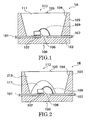
- Fig. 1 shows schematic cross-sectional view illustrating a configuration of the substantial part of a light emitting device according to the first embodiment of the invention.
- the light emitting device 1A shown here includes a resin stem 100, a semiconductor light emitting element 106 mounted on the resin stem 100 and a sealing element 111 provided to embed the element 106.
- the resin stem 100 includes leads 101, 102 shaped from a lead frame, and a resin portion 103 molded integrally with the leads 101, 102.
- the resin portion 103 is typically made of a thermoplastic resin preferably, for example, of a nylon system having inert coupling radicals.
- the thermoplastic resin may be a resin having a high resistance to heat, such as liquid crystal polymer (LCP), polyphenylene sulfide (PPS: thermoplastic resin) or syndiotactic polystyrene (SPS: crystalline polystyrene).
- LCP liquid crystal polymer
- PPS polyphenylene sulfide
- SPS syndiotactic polystyrene
- the plan-viewed outer configuration of the resin portion 103 may be a substantial square approximately sized 2.0 ⁇ 2.0mm through 6.0 ⁇ 6.0mm, or a substantial rectangular approximately sized 2.0 ⁇ 3.0mm through 5.0 ⁇ 7.0mm.
- the leads 101, 102 have opposed ends close to each other, and extend therefrom in the opposite directions to outside the resin portion 103.
- the resin portion 103 has formed an opening 105, and the semiconductor light emitting element 106 is mounted at the bottom of the opening 105.
- the plan-viewed shape of the opening 105 can be circular of approximately elliptical or approximately elongate-circular.
- the inner wall surface of the resin portion 103 surrounding the element 106 inclines to face toward the light extraction direction to function as a reflective surface 104 for reflecting light.
- the light emitting element 106 is placed to deviate from the center of the bottom surface of the opening 105.
- the reason of this off-center arrangement is to ensure a enough space for boding wire 109, and to realize a high optical output by increasing the reflection efficiency by placing the element 106 close to the reflective surface 104.
- the light emitting element 106 is mounted by an adhesive 107 such as silver (Ag) paste onto a lead 101 which is placed at the bottom of the opening 105.
- the element 106 has a electrode (not shown) on its surface, and is connected with the lead 102 by a bonding wire 109 such as a gold (Au) wire.
- the invention uses a silicone resin instead of a conventional epoxy resin as the sealing element 111 filling the opening 105.
- silicone resins are less fragile and less subjected to cracks.
- Silicone resins usable in the present invention exhibit a high bonding force with the resin portion 103 made of a thermoplastic resin, for example, and a high moisture resistance. Additionally, they do not crack or exfoliate so much due to a temperature stress. Furthermore, such a silicone resin filled in the opening produces only a remarkably small resin stress to the light emitting element 106 and the Au wire 109.
- silicone resins are more resistance to light irradiated from the light emitting element 106 than epoxy resins.
- Rubber-like silicone resins have a JISA hardness in the range of approximately 50 to 90.
- Epoxy resins widely used as the sealing element materials in conventional light emitting devices have a JISA hardness around 95.
- the light emitting device as shown in Fig. 1 is used as a "surface-mounting type" lamp, for example, and mounted on a packaging substrate with an assembly apparatus. In this process, a vacuum collet of the assembly apparatus is often pressed against the surface of the sealing element 111.
- the sealing element 111 may be deformed by the pressing force from the vacuum collet, which in turn may deform the wire 109 or give a stress to the light emitting element 106.
- rubber-like silicone resins having a JISA hardness in the range of 50 to 90 are prevented from deformation by a selector or an assembler used for selecting or assembling light emitting devices.
- a technique for increasing the hardness of a silicone resin is to add an agent for giving a thixotropy index.
- a silicone resin Upon burying a silicone resin, it is poured into the opening 105 of the resin stem through a thin nozzle, and thereafter cured. In this process, it is preferable to use a silicone resin having a pre-curing viscosity around 100cp through 10000cp. Thereby, it is possible to fully bury the opening including narrow spaces and to limit the residual stress upon curing within a sufficiently low range, without giving an excessive stress to the light emitting element 106 and the wire 109.
- the Inventor prepared light emitting devices according to the embodiment as shown in Fig. 1 by using a rubber-like silicone resin having the pre-during viscosity of 1000cp and post-curing JISA hardness value of 70, and carried out a temperature cycle test in the temperature range from -40°C to 110°C.
- a temperature cycle test in the temperature range from -40°C to 110°C.
- a silicone resin in particular, a rubber-like silicone resin, reduces the possibility of cracks and exfoliation that often occurred in conventional epoxy resins, breakage of wires, and so on.
- the Inventor has found that the optical output efficiency of the light emitting device can be improved by using the silicone resin. That is, the Inventor has found a substantially transparent resin material among the silicone resin, especially among the rubber-like silicone resin, which can be used in the present invention. By using such a transparent silicone resin, the optical output efficiency of the light emitted from the light emitting element 106 can be improved. As a result, a brighter light emitting device can be realized.
- silicone resin also improves the durability against light emitted from the semiconductor light emitting element 106 or light intruding from the exterior of the light emitting device. Epoxy resins change in color when exposed to light, and even if it is initially transparent, its optical transmittance decreases after long-time use.
- silicone resin leads to a very satisfactory result. That is, if a silicone resin is used, change or color and other types of deterioration do not occur even after it is exposed to short wavelength light such as ultraviolet rays. That is, the silicone resin can maintain its initial transparent state for a long period. Therefore, silicone resins contribute to realization of light emitting devices exhibiting excellent resistance to light and weather, and contribute to keep a high external output efficiency for a long period.
- the resin portion 103 may be equipped with optical reflectivity.
- the resin portion 103 may be made of 65 or more weight % of a thermoplastic resin and 35 or less weight % of a filling agent.
- the filling agent contains a, high-reflective material such as titanium oxide (TiO 3 ), silicon oxide, aluminum oxide, silica or alumina. In case of titanium oxide, its content is in the range from 10 to 15%.
- TiO 3 titanium oxide
- the reflective surface 104 is a part of the resin portion containing a diffusing material that reflects light, it can reflect light from the light emitting element 106 and the fluorescent element 110 upward to realize a high luminance of the light emitting device. If the reflective surface 104 is configured as a paraboloid of revolution, for example, the output and the quality of the light emitting device can be further improved.
- present invention is not limited to this specific example, but can be applied to all types of light emitting deices which has a structure where a semiconductor light emitting element is sealed by a resin.
- Fig. 2 is a cross-sectional view that schematically shows the second specific example of the light emitting device according to the invention.
- Fig. 1 the same or equivalent components as those already explained with reference to Fig. 1 are commonly labeled, and their detailed explanation is omitted for simplicity.
- the light emitting device 1B shown here also includes a resin stem 100, semiconductor light emitting element 106 mounted thereon, and sealing element 111 of a silicone resin provided to embed the element 106.
- the sealing element 111 merely embeds the light emitting element 106, and a second sealing element 213 of a transparent resin is provided outside the sealing element 111.
- the second sealing element 213 may be made of an epoxy resin, silicone resin or any of other various materials.
- the second sealing element 213 may be colored, and any material adaptable to the dye or coloring agent used can be selected.
- the second sealing element 213 may contain a diffusing material dispersed therein to scatter light. In this case, light can be diffused, and broader light distribution characteristics can be obtained.
- a silicone resin is used as the second sealing element 213, then its close contact with the sealing element 111 is enhanced, and the moisture resistance is improved.
- the sealing element 111 made of a silicone resin wraps the entirety of the Au wire 109. Therefore, a reliable light emitting element free from breakage of wire due to a resin stress can be realized. If the wire partly projects into the second sealing element 213, it will readily break due to a stress produced at the interface between the sealing elements 111, 213. In this specific example, however, since the wire 109 is entirely embedded by the sealing element 111, it is free from breakage.
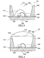
- Fig. 3 is a cross-sectional view that schematically shows the third specific example of the light emitting device according to the invention.
- the same or equivalent components as those already explained with reference to Figs. 1 and 2 are commonly labeled, and their detailed explanation is omitted for simplicity.
- the light emitting device 1C shown here also includes a resin stem 100, semiconductor light emitting element 106 mounted thereon, and sealing element 111 provided to embed the element 106.
- the sealing element 111 merely embeds the light emitting element 106. In this specific example, however, the space outside the sealing element 111 remains open, without being filled by any other sealing element.
- the limitative use of the sealing element 111 only to enclose the light emitting element 106 mounted at the bottom of the opening 105 contributes to small-sizing the emitting portion. Therefore, the luminance increases, and the function of the reflective surface 104 to gather rays of light is enhanced.
- the approximately hemispheric sealing element 111 serves as the emission point, and the reflective surface 104 surrounds it, the same optically converging effect as a conventional lamp can be obtained.
- the sealing element 111 embeds the entirety of the Au wires 108, 109, it prevents breakage of wire by a resin stress, and ensures a high reliability.
- Fig. 4 is a cross-sectional view that schematically shows the fourth specific example of the light emitting device according to the invention.
- the light emitting device 1D shown here also includes a resin stem 100, semiconductor light emitting element 106 mounted thereon, and sealing element 111 embedding the element 106.
- the embodiment shown here includes a convex transparent element 413 is provided on the sealing element 111 to ensure the function of gathering rays of light.
- the transparent element 413 may be made of a resin, for example.
- a silicone resin is advantageous for decreasing the difference of the refractive index from the sealing element 111 and to reduce the loss by reflection at the interface with the sealing element 111.
- the convex shape of the transparent element 413 is not limited to a spherical shape. Any appropriate shape can be selected depending on the required converging ratio or luminous intensity profile.
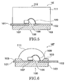
- Fig. 5 is a cross-sectional view that schematically shows a fifth example of a light emitting device of the invention.
- the same or equivalent components as those already explained with reference to Figs. 1 through 4 are commonly labeled, and their detailed explanation is omitted for simplicity.
- the light emitting device 1E shown here also includes a resin stem 100, semiconductor light emitting element 106 mounted thereon, and sealing element 111 embedding the stacked structure.
- the sealing element 111 is made of silicone resin having a hardness in a range from 50 through 90 in JISA value.
- the resin portion 103 has no side wall around the sealing element 111 such that the light from the element 106 both upwardly and laterally to realize a wide luminous intensity profile. This is suitable for applications expected to provide a wide field of view or a wide field of emission.
- Shapes of the sealing element and the resin stem 100 are not limited to those illustrated.
- the sealing element may be hemispherical as shown in Fig. 6, and the resin stem 100 may have a resin portion 103 configured to bury the leads 101, 102 and surround the element with a low side wall.
- Fig. 7 is a cross-sectional view that schematically shows a sixth example of a light emitting device according to the invention.
- the same or equivalent components as those already explained with reference to Figs. 1 through 6 are commonly labeled, and their detailed explanation is omitted for simplicity.
- the light emitting device IF shown here also includes a pair of leads 101, 102.
- the first lead 101 has formed a cup portion 601 at the distal end, and the stacked structure including the light emitting element 106 is mounted at the bottom of the cup portion 601. Then the wire 109 extending from the element 106 is connected to the lead 102.
- the sealing element 111 is formed to embed these components.
- the sealing element 111 is made of silicone resin having a hardness in a range from 50 through 90 in JISA value.
- the inner side wall surface of the cup portion 601 serves as the reflective surface to reflect the primary light from the light emitting element 106 upwardly.
- the transparent sealing element 111 can function as a convex lens to converge the light emitted from the element 106.
- the light emitting device shown here replaces conventional lamp-type semiconductor devices, and is operative as a general-purpose light emitting device having a relatively wide field of emission.
- Fig. 8 is a cross-sectional view that schematically shows a seventh example of a light emitting device according to the invention.
- the same or equivalent components as those already explained with reference to Figs. 1 through 7 are commonly labeled, and their detailed explanation is omitted for simplicity.
- the light emitting device 1G shown here has a structure similar to the light emitting device 1F shown in fig. 7.
- the light emitting device 1G also has a cup portion 601 at the distal end of the first lead 101, and the light emitting element 106 is mounted at the bottom thereof. Then the wire 109 from the element 106 is connected to the lead 102.
- the sealing element 111 is made of silicone resin having a hardness in a range from 50 through 90 in JISA value. The sealing element 111 is provided to embed those components.
- the sealing element 111 is small-sized, and a transparent element 713 is provided to enclose the sealing element 111.
- the small-sized sealing element 111 diminishes the emission portion and increases the luminance.
- the top surface of the transparent element 713 functions as a lens to gather rays of light, and makes it possible to extract converged light as well.
- the transparent element 713 enclosing the sealing element 111 isolates the element 111 from the outside atmosphere and improves its durability against moisture and corrosive atmosphere.
- the transparent element may be made of a resin. Especially, an epoxy resin or silicone resin is advantageous for close contact with the sealing element 111 to enhance the resistance to whether and the mechanical strength.
- the sealing element 111 may be limited only on the cup portion 601 to reduce the size of the emission portion and thereby increase the luminance.
- the wire 109 will extend beyond the boundary between the sealing element 111 and the transparent element 713.
- the sealing element 111 and the transparent element 713 are made of similar materials, the stress at the boundary will be minimized and will prevent breakage of wire.
Landscapes
- Led Device Packages (AREA)
Abstract
Description
Claims (9)
- A light emitting device comprising:a semiconductor light emitting element; anda silicone resin provided to embed said semiconductor light emitting element, said silicone resin having a hardness not lower than 50 in JISA value.
- A light emitting device according to claim 1, wherein said silicone resin has a hardness not higher than 90 in JISA value.
- A light emitting device according to claim 1, wherein said silicone resin has a pre-curing viscosity in the range not lower than 100cp and not higher than 10000cp.
- A light emitting device according to claim 1, further comprising a wire connected to said semiconductor light emitting element,
said silicone resin being provided to embed said wire as well. - A light emitting device according to claim 1, further comprising a resin stem having a pair of leads and a resin portion burying at least a part of said pair of leads,
said semiconductor light emitting element being mounted on one of said pair of leads. - A light emitting device according to claim 5, wherein said resin portion has an opening,said semiconductor light emitting element being mounted on one of said pair of leads at the bottom of said opening,said silicone resin being provided in said opening.
- A light emitting device according to claim 5, wherein said resin portion is made of a thermoplastic resin.
- A light emitting device according to claim 6, wherein said opening has an inner side wall which inclines to face toward the open end,
said resin portion containing a material which reflects visible light. - A light emitting device according to claim 1, wherein said silicone resin is substantially transparent to a light emitted from said semiconductor light emitting element.
Applications Claiming Priority (2)
| Application Number | Priority Date | Filing Date | Title |
|---|---|---|---|
| JP2001110675 | 2001-04-09 | ||
| JP2001110675A JP2002314139A (en) | 2001-04-09 | 2001-04-09 | Light emitting device |
Publications (4)
| Publication Number | Publication Date |
|---|---|
| EP1249875A2 true EP1249875A2 (en) | 2002-10-16 |
| EP1249875A3 EP1249875A3 (en) | 2007-12-19 |
| EP1249875B1 EP1249875B1 (en) | 2011-02-16 |
| EP1249875B2 EP1249875B2 (en) | 2019-02-20 |
Family
ID=18962398
Family Applications (1)
| Application Number | Title | Priority Date | Filing Date |
|---|---|---|---|
| EP02007380.5A Expired - Lifetime EP1249875B2 (en) | 2001-04-09 | 2002-04-09 | Light emitting device |
Country Status (6)
| Country | Link |
|---|---|
| US (1) | US6710377B2 (en) |
| EP (1) | EP1249875B2 (en) |
| JP (1) | JP2002314139A (en) |
| CN (1) | CN1262023C (en) |
| DE (1) | DE60239173D1 (en) |
| TW (1) | TW552722B (en) |
Cited By (9)
| Publication number | Priority date | Publication date | Assignee | Title |
|---|---|---|---|---|
| DE20301627U1 (en) | 2003-01-30 | 2003-04-17 | OSA Opto Light GmbH, 12555 Berlin | Optoelectronic component for non axial use has light emitting diode placed non centrally on a carrier beneath transparent dome |
| WO2007009528A1 (en) * | 2005-07-21 | 2007-01-25 | Wacker Chemie Ag | Silicone resin potting of light-emitting diodes |
| WO2008145718A1 (en) * | 2007-06-01 | 2008-12-04 | Wacker Chemie Ag | Silicon moulded part comprising luminous bodies |
| US7666969B2 (en) | 2006-05-11 | 2010-02-23 | Wacker Chemie Ag | Silicone resin coating for electronic components |
| US8227821B2 (en) | 2004-09-22 | 2012-07-24 | Osram Opto Semiconductors Gmbh | Housing for an optoelectronic component, optoelectronic component and method for the production of an optoelectronic component |
| EP1786045A3 (en) * | 2005-11-15 | 2012-08-29 | Samsung LED Co., Ltd. | LED package |
| DE102011100028A1 (en) * | 2011-04-29 | 2012-10-31 | Osram Opto Semiconductors Gmbh | Component and method for manufacturing a device |
| WO2020109023A1 (en) * | 2018-11-29 | 2020-06-04 | Lumileds Holding B.V. | Light-emitting device and method of packaging the same |
| US11600754B2 (en) | 2018-11-29 | 2023-03-07 | Lumileds Llc | Light-emitting device and method of packaging the same |
Families Citing this family (68)
| Publication number | Priority date | Publication date | Assignee | Title |
|---|---|---|---|---|
| DE10033502A1 (en) * | 2000-07-10 | 2002-01-31 | Osram Opto Semiconductors Gmbh | Optoelectronic module, process for its production and its use |
| JP2002314138A (en) * | 2001-04-09 | 2002-10-25 | Toshiba Corp | Light emitting device |
| JP4101468B2 (en) * | 2001-04-09 | 2008-06-18 | 豊田合成株式会社 | Method for manufacturing light emitting device |
| US7244965B2 (en) * | 2002-09-04 | 2007-07-17 | Cree Inc, | Power surface mount light emitting die package |
| DE10307800A1 (en) * | 2003-02-24 | 2004-09-02 | Vishay Semiconductor Gmbh | Semiconductor device |
| TW200427111A (en) | 2003-03-12 | 2004-12-01 | Shinetsu Chemical Co | Material for coating/protecting light-emitting semiconductor and the light-emitting semiconductor device |
| JP4599857B2 (en) * | 2003-04-24 | 2010-12-15 | 日亜化学工業株式会社 | Semiconductor device and manufacturing method thereof |
| JP4645071B2 (en) * | 2003-06-20 | 2011-03-09 | 日亜化学工業株式会社 | Package molded body and semiconductor device using the same |
| JP4586967B2 (en) * | 2003-07-09 | 2010-11-24 | 信越化学工業株式会社 | Light emitting semiconductor coating protective material and light emitting semiconductor device |
| TWI373150B (en) | 2003-07-09 | 2012-09-21 | Shinetsu Chemical Co | Silicone rubber composition, light-emitting semiconductor embedding/protecting material and light-emitting semiconductor device |
| US6995402B2 (en) * | 2003-10-03 | 2006-02-07 | Lumileds Lighting, U.S., Llc | Integrated reflector cup for a light emitting device mount |
| US7276782B2 (en) * | 2003-10-31 | 2007-10-02 | Harvatek Corporation | Package structure for semiconductor |
| WO2005043636A1 (en) * | 2003-11-04 | 2005-05-12 | Shin-Etsu Handotai Co., Ltd. | Light emitting element |
| JP4803339B2 (en) | 2003-11-20 | 2011-10-26 | 信越化学工業株式会社 | Epoxy / silicone hybrid resin composition and light emitting semiconductor device |
| US7329904B2 (en) * | 2004-01-30 | 2008-02-12 | Toyoda Gosei Co., Ltd. | LED lamp device |
| JP4300418B2 (en) | 2004-04-30 | 2009-07-22 | 信越化学工業株式会社 | Epoxy / silicone hybrid resin composition and light emitting semiconductor device |
| US20050280016A1 (en) * | 2004-06-17 | 2005-12-22 | Mok Thye L | PCB-based surface mount LED device with silicone-based encapsulation structure |
| US20060006791A1 (en) * | 2004-07-06 | 2006-01-12 | Chia Chee W | Light emitting diode display that does not require epoxy encapsulation of the light emitting diode |
| US20060046327A1 (en) * | 2004-08-30 | 2006-03-02 | Nan Ya Plastics Corporation | High heat dissipation LED device and its manufacturing method |
| KR100709890B1 (en) * | 2004-09-10 | 2007-04-20 | 서울반도체 주식회사 | LED Package with Multiple Molding Resins |
| EP1794808B1 (en) | 2004-09-10 | 2017-08-09 | Seoul Semiconductor Co., Ltd. | Light emitting diode package having multiple molding resins |
| DE102005043928B4 (en) * | 2004-09-16 | 2011-08-18 | Sharp Kk | Optical semiconductor device and method for its production |
| TWI405349B (en) | 2004-10-07 | 2013-08-11 | 首爾半導體股份有限公司 | Side illumination lens and light-emitting element using the same |
| CN100382287C (en) * | 2004-10-12 | 2008-04-16 | 宏齐科技股份有限公司 | Semiconductor packaging structure |
| US20060092644A1 (en) * | 2004-10-28 | 2006-05-04 | Mok Thye L | Small package high efficiency illuminator design |
| JP4634810B2 (en) * | 2005-01-20 | 2011-02-16 | 信越化学工業株式会社 | Silicone sealed LED |
| US7859006B2 (en) | 2005-02-23 | 2010-12-28 | Mitsubishi Chemical Corporation | Semiconductor light emitting device member, method for manufacturing such semiconductor light emitting device member and semiconductor light emitting device using such semiconductor light emitting device member |
| JP5694875B2 (en) * | 2005-02-23 | 2015-04-01 | 三菱化学株式会社 | SEMICONDUCTOR LIGHT EMITTING DEVICE MEMBER, ITS MANUFACTURING METHOD, AND SEMICONDUCTOR LIGHT EMITTING DEVICE USING THE SAME |
| CN100377376C (en) * | 2005-03-21 | 2008-03-26 | 亿光电子工业股份有限公司 | Method for manufacturing light-emitting diode reflecting cover |
| JP2006269531A (en) * | 2005-03-22 | 2006-10-05 | Matsushita Electric Ind Co Ltd | Optical semiconductor device |
| JP4744178B2 (en) * | 2005-04-08 | 2011-08-10 | シャープ株式会社 | Light emitting diode |
| US20060270808A1 (en) * | 2005-05-24 | 2006-11-30 | Shin-Etsu Chemical Co., Ltd. | Epoxy-silicone mixed resin composition, cured article thereof, and light-emitting semiconductor device |
| US7952108B2 (en) * | 2005-10-18 | 2011-05-31 | Finisar Corporation | Reducing thermal expansion effects in semiconductor packages |
| JP2007194401A (en) * | 2006-01-19 | 2007-08-02 | Showa Denko Kk | LED package using compound semiconductor light emitting device |
| US8044412B2 (en) | 2006-01-20 | 2011-10-25 | Taiwan Semiconductor Manufacturing Company, Ltd | Package for a light emitting element |
| JP5141107B2 (en) * | 2006-06-27 | 2013-02-13 | 三菱化学株式会社 | Lighting device |
| WO2008001799A1 (en) | 2006-06-27 | 2008-01-03 | Mitsubishi Chemical Corporation | Illuminating device |
| JP5205724B2 (en) * | 2006-08-04 | 2013-06-05 | 日亜化学工業株式会社 | Light emitting device |
| US20080049445A1 (en) * | 2006-08-25 | 2008-02-28 | Philips Lumileds Lighting Company, Llc | Backlight Using High-Powered Corner LED |
| KR101258227B1 (en) | 2006-08-29 | 2013-04-25 | 서울반도체 주식회사 | Light emitting device |
| KR100828900B1 (en) | 2006-09-04 | 2008-05-09 | 엘지이노텍 주식회사 | Light emitting diode package and manufacturing method thereof |
| JP5380774B2 (en) | 2006-12-28 | 2014-01-08 | 日亜化学工業株式会社 | Surface mount type side surface light emitting device and manufacturing method thereof |
| KR101119172B1 (en) * | 2007-02-05 | 2012-03-21 | 삼성전자주식회사 | Light emitting diode module and display device using the same |
| JP5052326B2 (en) * | 2007-10-31 | 2012-10-17 | シャープ株式会社 | Chip component type LED and manufacturing method thereof |
| DE102008014122A1 (en) | 2007-11-29 | 2009-06-04 | Osram Opto Semiconductors Gmbh | Method for producing an optoelectronic component and optoelectronic component |
| JP5136963B2 (en) * | 2008-03-24 | 2013-02-06 | 信越化学工業株式会社 | Curable silicone rubber composition and semiconductor device |
| JP2010031149A (en) | 2008-07-29 | 2010-02-12 | Shin-Etsu Chemical Co Ltd | Resin composition for sealing optical semiconductor device |
| RU2509393C2 (en) * | 2008-10-17 | 2014-03-10 | Конинклейке Филипс Электроникс Н.В. | Light-emitting device |
| TWI384591B (en) * | 2008-11-17 | 2013-02-01 | 億光電子工業股份有限公司 | LED circuit board |
| JP5333758B2 (en) | 2009-02-27 | 2013-11-06 | 東芝ライテック株式会社 | Lighting device and lighting fixture |
| US20100289055A1 (en) * | 2009-05-14 | 2010-11-18 | Avago Technologies Ecbu Ip (Singapore) Pte. Ltd. | Silicone leaded chip carrier |
| JP5305452B2 (en) | 2009-06-12 | 2013-10-02 | 信越化学工業株式会社 | Resin composition for optical semiconductor element sealing |
| JP5354191B2 (en) * | 2009-06-30 | 2013-11-27 | 東芝ライテック株式会社 | Light bulb shaped lamp and lighting equipment |
| JP2011049527A (en) | 2009-07-29 | 2011-03-10 | Toshiba Lighting & Technology Corp | Led lighting equipment |
| US8678618B2 (en) | 2009-09-25 | 2014-03-25 | Toshiba Lighting & Technology Corporation | Self-ballasted lamp having a light-transmissive member in contact with light emitting elements and lighting equipment incorporating the same |
| JP5257622B2 (en) | 2010-02-26 | 2013-08-07 | 東芝ライテック株式会社 | Light bulb shaped lamp and lighting equipment |
| JP5489280B2 (en) | 2010-04-07 | 2014-05-14 | 信越化学工業株式会社 | Epoxy composition for optical semiconductor encapsulation |
| JP2012019062A (en) | 2010-07-08 | 2012-01-26 | Shin Etsu Chem Co Ltd | Light emitting semiconductor device, mounting board, and method for manufacturing the light emitting semiconductor device and the mounting board |
| KR101626412B1 (en) | 2010-12-24 | 2016-06-02 | 삼성전자주식회사 | Light emitting device package and method of manufacturing the same |
| KR101830717B1 (en) * | 2011-06-30 | 2018-02-21 | 엘지이노텍 주식회사 | A light emitting device pakage |
| JP5682497B2 (en) * | 2011-07-29 | 2015-03-11 | 信越化学工業株式会社 | Method for manufacturing surface-mounted light-emitting device and reflector substrate |
| CN102623623A (en) * | 2012-03-26 | 2012-08-01 | 李海涛 | Surface-mounted type LED (light-emitting diode) device with inner core protected by flexible rubber |
| JP5721668B2 (en) * | 2012-06-29 | 2015-05-20 | シャープ株式会社 | LIGHT EMITTING DEVICE, LIGHTING DEVICE, AND DISPLAY DEVICE BACKLIGHT |
| JP2014120515A (en) * | 2012-12-13 | 2014-06-30 | Shin Etsu Chem Co Ltd | Substrate for optical semiconductor device and method of manufacturing the same, aggregate substrate, and optical semiconductor device and method of manufacturing the same |
| JP6707369B2 (en) | 2015-03-30 | 2020-06-10 | ダウ・東レ株式会社 | Silicone material, curable silicone composition, and optical device |
| CN105316564B (en) * | 2015-06-08 | 2017-05-17 | 天津达祥精密工业有限公司 | High-nickel austenite nodular cast iron production process adopting wire-feeding spheroidizing |
| JP6679306B2 (en) * | 2015-12-28 | 2020-04-15 | シャープ株式会社 | Method of manufacturing light emitting device |
| CN114784170A (en) * | 2022-04-14 | 2022-07-22 | 佛山市国星光电股份有限公司 | LED support, preparation method of support, light-emitting device and support array |
Family Cites Families (17)
| Publication number | Priority date | Publication date | Assignee | Title |
|---|---|---|---|---|
| JPS6254974A (en) * | 1985-09-04 | 1987-03-10 | Mitsubishi Electric Corp | Optical coupling semiconductor device |
| JP2715792B2 (en) * | 1992-02-13 | 1998-02-18 | 信越化学工業株式会社 | Light transmitting epoxy resin composition and optical semiconductor device |
| JPH065742A (en) * | 1992-06-22 | 1994-01-14 | Mitsubishi Electric Corp | Semiconductor device, resin used for sealing the same, and method of manufacturing semiconductor device |
| JPH07111343A (en) * | 1993-10-13 | 1995-04-25 | Matsushita Electron Corp | Photoelectric device |
| DE69428578T2 (en) * | 1993-12-16 | 2002-06-27 | Sharp K.K., Osaka | Manufacturing method for semiconductor light emitting devices |
| JP3648756B2 (en) * | 1994-03-22 | 2005-05-18 | Jsr株式会社 | Coating material for semiconductor devices |
| JPH07278438A (en) * | 1994-04-14 | 1995-10-24 | Toray Dow Corning Silicone Co Ltd | Curable organopolysiloxane composition for impregnation of electronic parts and electronic parts |
| US5832600A (en) * | 1995-06-06 | 1998-11-10 | Seiko Epson Corporation | Method of mounting electronic parts |
| JP3393247B2 (en) * | 1995-09-29 | 2003-04-07 | ソニー株式会社 | Optical device and method of manufacturing the same |
| JPH09246423A (en) * | 1996-03-13 | 1997-09-19 | Hitachi Ltd | Semiconductor device |
| JP3034363U (en) * | 1996-05-01 | 1997-02-18 | 武雄 稲垣 | Indicator with built-in light emitting element |
| US6274890B1 (en) * | 1997-01-15 | 2001-08-14 | Kabushiki Kaisha Toshiba | Semiconductor light emitting device and its manufacturing method |
| JP3492178B2 (en) * | 1997-01-15 | 2004-02-03 | 株式会社東芝 | Semiconductor light emitting device and method of manufacturing the same |
| TW414924B (en) * | 1998-05-29 | 2000-12-11 | Rohm Co Ltd | Semiconductor device of resin package |
| JP3618551B2 (en) * | 1998-06-30 | 2005-02-09 | 株式会社東芝 | Optical semiconductor module |
| JP2000156528A (en) * | 1998-11-19 | 2000-06-06 | Sharp Corp | Light emitting element |
| JP3613041B2 (en) * | 1998-12-16 | 2005-01-26 | 日亜化学工業株式会社 | Light emitting device and manufacturing method thereof |
-
2001
- 2001-04-09 JP JP2001110675A patent/JP2002314139A/en active Pending
-
2002
- 2002-04-04 TW TW091106884A patent/TW552722B/en active
- 2002-04-09 CN CNB02106198XA patent/CN1262023C/en not_active Expired - Fee Related
- 2002-04-09 US US10/119,413 patent/US6710377B2/en not_active Expired - Lifetime
- 2002-04-09 EP EP02007380.5A patent/EP1249875B2/en not_active Expired - Lifetime
- 2002-04-09 DE DE60239173T patent/DE60239173D1/en not_active Expired - Lifetime
Cited By (10)
| Publication number | Priority date | Publication date | Assignee | Title |
|---|---|---|---|---|
| DE20301627U1 (en) | 2003-01-30 | 2003-04-17 | OSA Opto Light GmbH, 12555 Berlin | Optoelectronic component for non axial use has light emitting diode placed non centrally on a carrier beneath transparent dome |
| US8227821B2 (en) | 2004-09-22 | 2012-07-24 | Osram Opto Semiconductors Gmbh | Housing for an optoelectronic component, optoelectronic component and method for the production of an optoelectronic component |
| WO2007009528A1 (en) * | 2005-07-21 | 2007-01-25 | Wacker Chemie Ag | Silicone resin potting of light-emitting diodes |
| EP1786045A3 (en) * | 2005-11-15 | 2012-08-29 | Samsung LED Co., Ltd. | LED package |
| US7666969B2 (en) | 2006-05-11 | 2010-02-23 | Wacker Chemie Ag | Silicone resin coating for electronic components |
| WO2008145718A1 (en) * | 2007-06-01 | 2008-12-04 | Wacker Chemie Ag | Silicon moulded part comprising luminous bodies |
| DE102011100028A1 (en) * | 2011-04-29 | 2012-10-31 | Osram Opto Semiconductors Gmbh | Component and method for manufacturing a device |
| US9252344B2 (en) | 2011-04-29 | 2016-02-02 | Osram Opto Semiconductors Gmbh | Structural component and method for producing a structural component |
| WO2020109023A1 (en) * | 2018-11-29 | 2020-06-04 | Lumileds Holding B.V. | Light-emitting device and method of packaging the same |
| US11600754B2 (en) | 2018-11-29 | 2023-03-07 | Lumileds Llc | Light-emitting device and method of packaging the same |
Also Published As
| Publication number | Publication date |
|---|---|
| DE60239173D1 (en) | 2011-03-31 |
| TW552722B (en) | 2003-09-11 |
| JP2002314139A (en) | 2002-10-25 |
| CN1380704A (en) | 2002-11-20 |
| EP1249875B2 (en) | 2019-02-20 |
| US6710377B2 (en) | 2004-03-23 |
| EP1249875B1 (en) | 2011-02-16 |
| CN1262023C (en) | 2006-06-28 |
| US20020145152A1 (en) | 2002-10-10 |
| EP1249875A3 (en) | 2007-12-19 |
Similar Documents
| Publication | Publication Date | Title |
|---|---|---|
| EP1249875B1 (en) | Light emitting device | |
| US6747293B2 (en) | Light emitting device | |
| CN100550439C (en) | Semiconductor light emitting device and manufacturing method | |
| JP4599857B2 (en) | Semiconductor device and manufacturing method thereof | |
| CN102804426B (en) | light emitting device | |
| CN102113139B (en) | Light-emitting device | |
| CN100382345C (en) | Optical semiconductor device | |
| JP5695488B2 (en) | Luminous body package | |
| EP1741315B1 (en) | Light-emitting devices having multiple encapsulation layers with at least one of the encapsulation layers including nanoparticles and methods of forming the same | |
| JP5596901B2 (en) | Power light emitting die package having a reflective lens and method of manufacturing the same | |
| KR100927077B1 (en) | Optical semiconductor device and manufacturing method thereof | |
| EP0854523B1 (en) | Semiconductor light emitting device and its manufacturing method | |
| CN101523621A (en) | Housing for an optoelectronic device, optoelectronic device and method for producing a housing for an optoelectronic device | |
| CN100527454C (en) | Optoelectronic component and housing for an optoelectronic component | |
| JP2007329502A (en) | Light emitting device | |
| JP4403199B2 (en) | Light emitting device | |
| JP4600404B2 (en) | Semiconductor device and manufacturing method thereof | |
| JP3931916B2 (en) | Semiconductor device and manufacturing method thereof | |
| CN102194975B (en) | Optical semiconductor package and optical semiconductor device | |
| CN108369979A (en) | Electro-optical components | |
| KR20090049466A (en) | Lamp Type LED Package | |
| KR100848873B1 (en) | LED lamp and manufacturing method thereof | |
| KR20080024031A (en) | Light emitting diode package and manufacturing method thereof | |
| KR20090132087A (en) | LED Package |
Legal Events
| Date | Code | Title | Description |
|---|---|---|---|
| PUAI | Public reference made under article 153(3) epc to a published international application that has entered the european phase |
Free format text: ORIGINAL CODE: 0009012 |
|
| 17P | Request for examination filed |
Effective date: 20020409 |
|
| AK | Designated contracting states |
Kind code of ref document: A2 Designated state(s): AT BE CH CY DE DK ES FI FR GB GR IE IT LI LU MC NL PT SE TR |
|
| AX | Request for extension of the european patent |
Free format text: AL;LT;LV;MK;RO;SI |
|
| PUAL | Search report despatched |
Free format text: ORIGINAL CODE: 0009013 |
|
| AK | Designated contracting states |
Kind code of ref document: A3 Designated state(s): AT BE CH CY DE DK ES FI FR GB GR IE IT LI LU MC NL PT SE TR |
|
| AX | Request for extension of the european patent |
Extension state: AL LT LV MK RO SI |
|
| AKX | Designation fees paid |
Designated state(s): DE FR GB |
|
| 17Q | First examination report despatched |
Effective date: 20091021 |
|
| GRAP | Despatch of communication of intention to grant a patent |
Free format text: ORIGINAL CODE: EPIDOSNIGR1 |
|
| RIC1 | Information provided on ipc code assigned before grant |
Ipc: H01L 33/56 20100101AFI20100830BHEP Ipc: H01L 33/48 20100101ALN20100830BHEP |
|
| GRAS | Grant fee paid |
Free format text: ORIGINAL CODE: EPIDOSNIGR3 |
|
| GRAA | (expected) grant |
Free format text: ORIGINAL CODE: 0009210 |
|
| AK | Designated contracting states |
Kind code of ref document: B1 Designated state(s): DE FR GB |
|
| REG | Reference to a national code |
Ref country code: GB Ref legal event code: FG4D |
|
| REF | Corresponds to: |
Ref document number: 60239173 Country of ref document: DE Date of ref document: 20110331 Kind code of ref document: P |
|
| REG | Reference to a national code |
Ref country code: DE Ref legal event code: R096 Ref document number: 60239173 Country of ref document: DE Effective date: 20110331 |
|
| PLBI | Opposition filed |
Free format text: ORIGINAL CODE: 0009260 |
|
| 26 | Opposition filed |
Opponent name: HENKEL AG & CO. KGAA Effective date: 20111115 |
|
| PLAX | Notice of opposition and request to file observation + time limit sent |
Free format text: ORIGINAL CODE: EPIDOSNOBS2 |
|
| REG | Reference to a national code |
Ref country code: DE Ref legal event code: R026 Ref document number: 60239173 Country of ref document: DE Effective date: 20111115 |
|
| PLAF | Information modified related to communication of a notice of opposition and request to file observations + time limit |
Free format text: ORIGINAL CODE: EPIDOSCOBS2 |
|
| PLBB | Reply of patent proprietor to notice(s) of opposition received |
Free format text: ORIGINAL CODE: EPIDOSNOBS3 |
|
| PGFP | Annual fee paid to national office [announced via postgrant information from national office to epo] |
Ref country code: GB Payment date: 20120404 Year of fee payment: 11 |
|
| GBPC | Gb: european patent ceased through non-payment of renewal fee |
Effective date: 20130409 |
|
| APAH | Appeal reference modified |
Free format text: ORIGINAL CODE: EPIDOSCREFNO |
|
| APBM | Appeal reference recorded |
Free format text: ORIGINAL CODE: EPIDOSNREFNO |
|
| APBP | Date of receipt of notice of appeal recorded |
Free format text: ORIGINAL CODE: EPIDOSNNOA2O |
|
| PG25 | Lapsed in a contracting state [announced via postgrant information from national office to epo] |
Ref country code: GB Free format text: LAPSE BECAUSE OF NON-PAYMENT OF DUE FEES Effective date: 20130409 |
|
| APBQ | Date of receipt of statement of grounds of appeal recorded |
Free format text: ORIGINAL CODE: EPIDOSNNOA3O |
|
| REG | Reference to a national code |
Ref country code: FR Ref legal event code: PLFP Year of fee payment: 15 |
|
| PGFP | Annual fee paid to national office [announced via postgrant information from national office to epo] |
Ref country code: FR Payment date: 20160309 Year of fee payment: 15 |
|
| REG | Reference to a national code |
Ref country code: FR Ref legal event code: ST Effective date: 20171229 |
|
| PG25 | Lapsed in a contracting state [announced via postgrant information from national office to epo] |
Ref country code: FR Free format text: LAPSE BECAUSE OF NON-PAYMENT OF DUE FEES Effective date: 20170502 |
|
| APBU | Appeal procedure closed |
Free format text: ORIGINAL CODE: EPIDOSNNOA9O |
|
| PUAH | Patent maintained in amended form |
Free format text: ORIGINAL CODE: 0009272 |
|
| STAA | Information on the status of an ep patent application or granted ep patent |
Free format text: STATUS: PATENT MAINTAINED AS AMENDED |
|
| 27A | Patent maintained in amended form |
Effective date: 20190220 |
|
| AK | Designated contracting states |
Kind code of ref document: B2 Designated state(s): DE FR GB |
|
| REG | Reference to a national code |
Ref country code: DE Ref legal event code: R102 Ref document number: 60239173 Country of ref document: DE |
|
| PGFP | Annual fee paid to national office [announced via postgrant information from national office to epo] |
Ref country code: DE Payment date: 20210316 Year of fee payment: 20 |
|
| REG | Reference to a national code |
Ref country code: DE Ref legal event code: R071 Ref document number: 60239173 Country of ref document: DE |