EP1248142A2 - Nematische Flüssigkristallvorrichtung und Verfahren zu ihrer Herstellung - Google Patents
Nematische Flüssigkristallvorrichtung und Verfahren zu ihrer Herstellung Download PDFInfo
- Publication number
- EP1248142A2 EP1248142A2 EP02250944A EP02250944A EP1248142A2 EP 1248142 A2 EP1248142 A2 EP 1248142A2 EP 02250944 A EP02250944 A EP 02250944A EP 02250944 A EP02250944 A EP 02250944A EP 1248142 A2 EP1248142 A2 EP 1248142A2
- Authority
- EP
- European Patent Office
- Prior art keywords
- liquid crystal
- protrusions
- crystal device
- operating state
- anisotropic
- Prior art date
- Legal status (The legal status is an assumption and is not a legal conclusion. Google has not performed a legal analysis and makes no representation as to the accuracy of the status listed.)
- Granted
Links
Images




Classifications
-
- G—PHYSICS
- G02—OPTICS
- G02F—OPTICAL DEVICES OR ARRANGEMENTS FOR THE CONTROL OF LIGHT BY MODIFICATION OF THE OPTICAL PROPERTIES OF THE MEDIA OF THE ELEMENTS INVOLVED THEREIN; NON-LINEAR OPTICS; FREQUENCY-CHANGING OF LIGHT; OPTICAL LOGIC ELEMENTS; OPTICAL ANALOGUE/DIGITAL CONVERTERS
- G02F1/00—Devices or arrangements for the control of the intensity, colour, phase, polarisation or direction of light arriving from an independent light source, e.g. switching, gating or modulating; Non-linear optics
- G02F1/01—Devices or arrangements for the control of the intensity, colour, phase, polarisation or direction of light arriving from an independent light source, e.g. switching, gating or modulating; Non-linear optics for the control of the intensity, phase, polarisation or colour
- G02F1/13—Devices or arrangements for the control of the intensity, colour, phase, polarisation or direction of light arriving from an independent light source, e.g. switching, gating or modulating; Non-linear optics for the control of the intensity, phase, polarisation or colour based on liquid crystals, e.g. single liquid crystal display cells
- G02F1/137—Devices or arrangements for the control of the intensity, colour, phase, polarisation or direction of light arriving from an independent light source, e.g. switching, gating or modulating; Non-linear optics for the control of the intensity, phase, polarisation or colour based on liquid crystals, e.g. single liquid crystal display cells characterised by the electro-optical or magneto-optical effect, e.g. field-induced phase transition, orientation effect, guest-host interaction or dynamic scattering
- G02F1/139—Devices or arrangements for the control of the intensity, colour, phase, polarisation or direction of light arriving from an independent light source, e.g. switching, gating or modulating; Non-linear optics for the control of the intensity, phase, polarisation or colour based on liquid crystals, e.g. single liquid crystal display cells characterised by the electro-optical or magneto-optical effect, e.g. field-induced phase transition, orientation effect, guest-host interaction or dynamic scattering based on orientation effects in which the liquid crystal remains transparent
- G02F1/1391—Bistable or multi-stable liquid crystal cells
-
- G—PHYSICS
- G02—OPTICS
- G02F—OPTICAL DEVICES OR ARRANGEMENTS FOR THE CONTROL OF LIGHT BY MODIFICATION OF THE OPTICAL PROPERTIES OF THE MEDIA OF THE ELEMENTS INVOLVED THEREIN; NON-LINEAR OPTICS; FREQUENCY-CHANGING OF LIGHT; OPTICAL LOGIC ELEMENTS; OPTICAL ANALOGUE/DIGITAL CONVERTERS
- G02F1/00—Devices or arrangements for the control of the intensity, colour, phase, polarisation or direction of light arriving from an independent light source, e.g. switching, gating or modulating; Non-linear optics
- G02F1/01—Devices or arrangements for the control of the intensity, colour, phase, polarisation or direction of light arriving from an independent light source, e.g. switching, gating or modulating; Non-linear optics for the control of the intensity, phase, polarisation or colour
- G02F1/13—Devices or arrangements for the control of the intensity, colour, phase, polarisation or direction of light arriving from an independent light source, e.g. switching, gating or modulating; Non-linear optics for the control of the intensity, phase, polarisation or colour based on liquid crystals, e.g. single liquid crystal display cells
-
- G—PHYSICS
- G02—OPTICS
- G02F—OPTICAL DEVICES OR ARRANGEMENTS FOR THE CONTROL OF LIGHT BY MODIFICATION OF THE OPTICAL PROPERTIES OF THE MEDIA OF THE ELEMENTS INVOLVED THEREIN; NON-LINEAR OPTICS; FREQUENCY-CHANGING OF LIGHT; OPTICAL LOGIC ELEMENTS; OPTICAL ANALOGUE/DIGITAL CONVERTERS
- G02F1/00—Devices or arrangements for the control of the intensity, colour, phase, polarisation or direction of light arriving from an independent light source, e.g. switching, gating or modulating; Non-linear optics
- G02F1/01—Devices or arrangements for the control of the intensity, colour, phase, polarisation or direction of light arriving from an independent light source, e.g. switching, gating or modulating; Non-linear optics for the control of the intensity, phase, polarisation or colour
- G02F1/13—Devices or arrangements for the control of the intensity, colour, phase, polarisation or direction of light arriving from an independent light source, e.g. switching, gating or modulating; Non-linear optics for the control of the intensity, phase, polarisation or colour based on liquid crystals, e.g. single liquid crystal display cells
- G02F1/137—Devices or arrangements for the control of the intensity, colour, phase, polarisation or direction of light arriving from an independent light source, e.g. switching, gating or modulating; Non-linear optics for the control of the intensity, phase, polarisation or colour based on liquid crystals, e.g. single liquid crystal display cells characterised by the electro-optical or magneto-optical effect, e.g. field-induced phase transition, orientation effect, guest-host interaction or dynamic scattering
- G02F1/139—Devices or arrangements for the control of the intensity, colour, phase, polarisation or direction of light arriving from an independent light source, e.g. switching, gating or modulating; Non-linear optics for the control of the intensity, phase, polarisation or colour based on liquid crystals, e.g. single liquid crystal display cells characterised by the electro-optical or magneto-optical effect, e.g. field-induced phase transition, orientation effect, guest-host interaction or dynamic scattering based on orientation effects in which the liquid crystal remains transparent
- G02F1/1393—Devices or arrangements for the control of the intensity, colour, phase, polarisation or direction of light arriving from an independent light source, e.g. switching, gating or modulating; Non-linear optics for the control of the intensity, phase, polarisation or colour based on liquid crystals, e.g. single liquid crystal display cells characterised by the electro-optical or magneto-optical effect, e.g. field-induced phase transition, orientation effect, guest-host interaction or dynamic scattering based on orientation effects in which the liquid crystal remains transparent the birefringence of the liquid crystal being electrically controlled, e.g. ECB-, DAP-, HAN-, PI-LC cells
- G02F1/1395—Optically compensated birefringence [OCB]- cells or PI- cells
-
- G—PHYSICS
- G02—OPTICS
- G02F—OPTICAL DEVICES OR ARRANGEMENTS FOR THE CONTROL OF LIGHT BY MODIFICATION OF THE OPTICAL PROPERTIES OF THE MEDIA OF THE ELEMENTS INVOLVED THEREIN; NON-LINEAR OPTICS; FREQUENCY-CHANGING OF LIGHT; OPTICAL LOGIC ELEMENTS; OPTICAL ANALOGUE/DIGITAL CONVERTERS
- G02F1/00—Devices or arrangements for the control of the intensity, colour, phase, polarisation or direction of light arriving from an independent light source, e.g. switching, gating or modulating; Non-linear optics
- G02F1/01—Devices or arrangements for the control of the intensity, colour, phase, polarisation or direction of light arriving from an independent light source, e.g. switching, gating or modulating; Non-linear optics for the control of the intensity, phase, polarisation or colour
- G02F1/13—Devices or arrangements for the control of the intensity, colour, phase, polarisation or direction of light arriving from an independent light source, e.g. switching, gating or modulating; Non-linear optics for the control of the intensity, phase, polarisation or colour based on liquid crystals, e.g. single liquid crystal display cells
- G02F1/133—Constructional arrangements; Operation of liquid crystal cells; Circuit arrangements
- G02F1/1333—Constructional arrangements; Manufacturing methods
- G02F1/1337—Surface-induced orientation of the liquid crystal molecules, e.g. by alignment layers
-
- G—PHYSICS
- G02—OPTICS
- G02F—OPTICAL DEVICES OR ARRANGEMENTS FOR THE CONTROL OF LIGHT BY MODIFICATION OF THE OPTICAL PROPERTIES OF THE MEDIA OF THE ELEMENTS INVOLVED THEREIN; NON-LINEAR OPTICS; FREQUENCY-CHANGING OF LIGHT; OPTICAL LOGIC ELEMENTS; OPTICAL ANALOGUE/DIGITAL CONVERTERS
- G02F1/00—Devices or arrangements for the control of the intensity, colour, phase, polarisation or direction of light arriving from an independent light source, e.g. switching, gating or modulating; Non-linear optics
- G02F1/01—Devices or arrangements for the control of the intensity, colour, phase, polarisation or direction of light arriving from an independent light source, e.g. switching, gating or modulating; Non-linear optics for the control of the intensity, phase, polarisation or colour
- G02F1/13—Devices or arrangements for the control of the intensity, colour, phase, polarisation or direction of light arriving from an independent light source, e.g. switching, gating or modulating; Non-linear optics for the control of the intensity, phase, polarisation or colour based on liquid crystals, e.g. single liquid crystal display cells
- G02F1/133—Constructional arrangements; Operation of liquid crystal cells; Circuit arrangements
- G02F1/1333—Constructional arrangements; Manufacturing methods
- G02F1/1337—Surface-induced orientation of the liquid crystal molecules, e.g. by alignment layers
- G02F1/133707—Structures for producing distorted electric fields, e.g. bumps, protrusions, recesses, slits in pixel electrodes
-
- G—PHYSICS
- G02—OPTICS
- G02F—OPTICAL DEVICES OR ARRANGEMENTS FOR THE CONTROL OF LIGHT BY MODIFICATION OF THE OPTICAL PROPERTIES OF THE MEDIA OF THE ELEMENTS INVOLVED THEREIN; NON-LINEAR OPTICS; FREQUENCY-CHANGING OF LIGHT; OPTICAL LOGIC ELEMENTS; OPTICAL ANALOGUE/DIGITAL CONVERTERS
- G02F1/00—Devices or arrangements for the control of the intensity, colour, phase, polarisation or direction of light arriving from an independent light source, e.g. switching, gating or modulating; Non-linear optics
- G02F1/01—Devices or arrangements for the control of the intensity, colour, phase, polarisation or direction of light arriving from an independent light source, e.g. switching, gating or modulating; Non-linear optics for the control of the intensity, phase, polarisation or colour
- G02F1/13—Devices or arrangements for the control of the intensity, colour, phase, polarisation or direction of light arriving from an independent light source, e.g. switching, gating or modulating; Non-linear optics for the control of the intensity, phase, polarisation or colour based on liquid crystals, e.g. single liquid crystal display cells
- G02F1/133—Constructional arrangements; Operation of liquid crystal cells; Circuit arrangements
- G02F1/1333—Constructional arrangements; Manufacturing methods
- G02F1/1337—Surface-induced orientation of the liquid crystal molecules, e.g. by alignment layers
- G02F1/133711—Surface-induced orientation of the liquid crystal molecules, e.g. by alignment layers by organic films, e.g. polymeric films
- G02F1/133726—Surface-induced orientation of the liquid crystal molecules, e.g. by alignment layers by organic films, e.g. polymeric films made of a mesogenic material
-
- G—PHYSICS
- G02—OPTICS
- G02F—OPTICAL DEVICES OR ARRANGEMENTS FOR THE CONTROL OF LIGHT BY MODIFICATION OF THE OPTICAL PROPERTIES OF THE MEDIA OF THE ELEMENTS INVOLVED THEREIN; NON-LINEAR OPTICS; FREQUENCY-CHANGING OF LIGHT; OPTICAL LOGIC ELEMENTS; OPTICAL ANALOGUE/DIGITAL CONVERTERS
- G02F1/00—Devices or arrangements for the control of the intensity, colour, phase, polarisation or direction of light arriving from an independent light source, e.g. switching, gating or modulating; Non-linear optics
- G02F1/01—Devices or arrangements for the control of the intensity, colour, phase, polarisation or direction of light arriving from an independent light source, e.g. switching, gating or modulating; Non-linear optics for the control of the intensity, phase, polarisation or colour
- G02F1/13—Devices or arrangements for the control of the intensity, colour, phase, polarisation or direction of light arriving from an independent light source, e.g. switching, gating or modulating; Non-linear optics for the control of the intensity, phase, polarisation or colour based on liquid crystals, e.g. single liquid crystal display cells
- G02F1/133—Constructional arrangements; Operation of liquid crystal cells; Circuit arrangements
- G02F1/1333—Constructional arrangements; Manufacturing methods
- G02F1/1337—Surface-induced orientation of the liquid crystal molecules, e.g. by alignment layers
- G02F1/133753—Surface-induced orientation of the liquid crystal molecules, e.g. by alignment layers with different alignment orientations or pretilt angles on a same surface, e.g. for grey scale or improved viewing angle
-
- G—PHYSICS
- G02—OPTICS
- G02F—OPTICAL DEVICES OR ARRANGEMENTS FOR THE CONTROL OF LIGHT BY MODIFICATION OF THE OPTICAL PROPERTIES OF THE MEDIA OF THE ELEMENTS INVOLVED THEREIN; NON-LINEAR OPTICS; FREQUENCY-CHANGING OF LIGHT; OPTICAL LOGIC ELEMENTS; OPTICAL ANALOGUE/DIGITAL CONVERTERS
- G02F1/00—Devices or arrangements for the control of the intensity, colour, phase, polarisation or direction of light arriving from an independent light source, e.g. switching, gating or modulating; Non-linear optics
- G02F1/01—Devices or arrangements for the control of the intensity, colour, phase, polarisation or direction of light arriving from an independent light source, e.g. switching, gating or modulating; Non-linear optics for the control of the intensity, phase, polarisation or colour
- G02F1/13—Devices or arrangements for the control of the intensity, colour, phase, polarisation or direction of light arriving from an independent light source, e.g. switching, gating or modulating; Non-linear optics for the control of the intensity, phase, polarisation or colour based on liquid crystals, e.g. single liquid crystal display cells
- G02F1/133—Constructional arrangements; Operation of liquid crystal cells; Circuit arrangements
- G02F1/1333—Constructional arrangements; Manufacturing methods
- G02F1/1337—Surface-induced orientation of the liquid crystal molecules, e.g. by alignment layers
- G02F1/133776—Surface-induced orientation of the liquid crystal molecules, e.g. by alignment layers having structures locally influencing the alignment, e.g. unevenness
Definitions
- the invention relates to nematic liquid crystal devices formed with anisotropic protrusions, and methods of production thereof.
- the invention can be used to provide an improvement in obtaining and if necessary isolating the operating state of a pi-cell liquid crystal device at low voltages.
- the invention can also be applied to nucleating the operating states from the globally stable states in the BTN device, and for isolating the operating states from each other and from the globally stable state.
- the invention is particularly applicable to flat panel displays and pi-cells used in LCTV. Another application is in using BTN displays in mobile products.
- pi-Cell A Fast Liquid Crystal Optical Switching Device' 1984 Mol. Cryst. Liq. Cryst. Vol. 113, pp. 329-339 is a paper which introduces the pi-cell as a liquid crystal display mode that is fundamentally fast, since the symmetry of the device eliminates the adverse effects of a flow induced "backwards" torque exerted on the liquid crystal director towards the cell centre.
- the pi-cell has parallel surface tilt (the term “parallel” here referring to the rubbing directions at the two cell surfaces, rather than to the directors) such that at low voltages the splay (or H-) state is stable (see Figure 3b, page 332). At higher voltages switching takes place between a high and low voltage bend (or V-) state (see Figure 2b, page 331).
- EP 0,996,028 describes the generic use of nucleation regions to initiate the growth of the V-state from the H-state. Particular examples are given of the pi-cell device and the complementary negative pi-cell or SBD. As well as teaching patterned surface pre-tilt to generate these nucleation regions, it also teaches in-situ polymerisation of a nucleation region e.g. in the inter-pixel gaps. One technique described for patterning surface tilt is to use patterned reactive mesogen layers. These are however thin and do not protrude considerably into the liquid crystal.
- EP 0,965,876A2 describes the use of substantially homeotropic alignment to surround the active pixel area within a conventionally low surface pretilt pi-cell based display. At zero volts the surrounding substantially homeotropic alignment isolates the pixel from the reformation of the H-state; at zero volts then the pixel relaxes into the twist state (T-state) (see abstract column 2, page 3, lines 39-44 and claim 1). The device is operated at higher voltages in the V-state.
- Japanese Patent Application JP-A-9 90432 discloses the provision of nucleation sites within a pi-cell panel.
- the nucleation sites are provided by including spacer balls or pillars within the pi-cell panel and cooling the liquid crystal material from an isotropic phase to a nematic phase while an electric field is applied across the panel. This results in some of the spacer balls or pillars acting as nucleation sites for growth of the V-state. However the positioning of the spacers cannot be easily controlled.
- Japanese Patent Application JP-A-9 218411 discloses a LCD having a bend alignment state, which is stabilised, in the absence of an applied field, by the presence of spacers in the form of spherical particles.
- the spacers have a surface energy such that liquid crystal molecules adjacent the alignment layers are mainly aligned parallel to the alignment layers.
- a field has to be applied during the initial alignment of the device.
- the particles can not be positioned so as to be outside the pixel apertures so that the contrast ratio of the display is reduced by the presence of the particles.
- European Patent Application No. 00310110.2 describes the use of birefringent spacers (for example those made from polymerisable reactive mesogens) in a liquid crystal display, said spacers having the same optical characteristic as one of the states of the switched states of the liquid crystal display.
- variable parts are liquid crystal, whilst the invariable parts are fabricated from a birefringent material running between the top and bottom surfaces. These invariable parts act also as spacers.
- British Patent Application No. 9704623.9 describes a liquid crystal device in which at least one alignment layer has been fabricated from a mixture of mono-functional and di-functional reactive mesogens, the ratio of these materials acting to control the surface pre-tilt of the contiguous liquid crystal material. It teaches that as the percentage of mono-functional reactive mesogen is increased then the tilt at the RM/air interface is increased.
- US 5,995,184 describes the fabrication of thin film retardation plates from polymerisable reactive mesogens. It teaches the addition of an additive that migrates to the RM/air interface to modify the surface energy and hence control the tilt of the reactive mesogen molecules at that surface, in particular it teaches reducing the tilt angle at the RM/air interface.
- EP 0,880,052 describes the fabrication of multi-domain liquid crystal devices by using a patterned, thin, twisted reactive mesogen layer above a conventional alignment layer.
- Figure 5 of the British Application shows parallel alignment in the none reactive mesogen region and twisted alignment above the reactive mesogen region, the regions above the reactive mesogen are not used for nucleating an operating state from a zero voltage non-operating state. This is additionally supported by the regions above the RM being of the same area as regions not above the RM, and that the application explicitly teaches to make the RM layer as thin as possible.
- BTN bistable twisted nematic
- a BTN device is a slower device than a pi-cell, but is stable in the two states of ⁇ ⁇ 180°, hence the name bistable.
- a typical BTN device is referred to as having antiparallel alignment because the rubbing directions at the two liquid crystal surfaces are antiparallel. This actually results in the directors at the two surfaces of the liquid crystal being aligned parallel to each other.
- British Patent Application No. 9911730.1 describes the fabrication of BTN devices with an isolation region between neighbouring pixels, the isolation region is a HAN state, a uniform lying helix or a focal conic texture. It is formed through patterning the surface pretilt of the alignment layer, such that the pretilt of interpixel gaps is different from that of the intrapixel region.
- the antiparallel BTN has three possible stable twist states e.g. 0°, 180° and 360°, more generally: (phi-pi), phi and (phi+pi) twist states. With suitable addressing, two of these states can be accessed and used as operating states.
- the energy of the three stable twist states depends on the thickness-to-pitch (d/p) ration and differs, such that the lowest energy state, which is normally topologically distinct to the other two stable twist states, does not correspond to an operating state, e.g. phi. This results in the energetically favourable (but undesirable) state nucleating and growing over a period of time once the voltage is turned off. Even if this undesired state does not nucleate when the voltage is turned off, bistability is not possible without isolation because the more energetically favourable of the operating states will slowly grow into the other one.
- the invention makes use of surface protrusions made from anisotropic materials (in particular from polymerisable reactive mesogens) to nucleate and/or isolate an operating state of a liquid crystal device from a non-operating state.
- the invention is particularly (though not exclusively) applicable to nematic devices in which the operating state is topologically distinct from the stable state at zero field applied.
- One such device is the pi-cell in which the operating V-state must be nucleated from the low voltage H-state.
- Another such device is the BTN device which when used as a storage device requires isolation of the operating states from the global minimum state and from each other.
- EP 0,996,028 and EP 0,965,876 particularly teach modifying surface pretilt to obtain low voltage nucleation. However patterning just at an alignment layer can produce occasional failure (and hence reduced yield) due to disclination trapping at the surface.
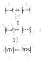
- Figure 1 is a schematic showing the orientation of directors 2 between substrates 4 and 6 in different states in the operation of a pi-cell, as described in the prior art documents mentioned above.
- Figure 2 is a schematic showing the orientation of directors 8 between substrates 10 and 12 in different states in the operation of a BTN device, as described in the prior art mentioned above.
- a first embodiment of the invention uses twisted anisotropic protrusions to nucleate V-state from H-state.
- indium tin oxide glass coated substrates 30 and 42 were coated, as known to those skilled in the art, with alignment layers 32 and 33 formed from SE610 (Nissan chemicals). Each substrate 30, 42 was then unidirectionally rubbed again as known to those skilled in the art.
- a mixture of 1:3 reactive mesogen RM257 (Merck) to toluene was spun at 1200rpm (at 80°C), the RM257 being previously doped with 1.2% CB15 (Merck) to form a protrusion layer 34.
- the RM257/CB15 protrusion layer 34 was UV cured through a mask 36 by UV radiation 38, and then rinsed in toluene to leave one substrate 30 coated with about 2.5 micron high twisted anisotropic protrusions 40, as shown in Figure 3c.
- This substrate 30 was then fabricated into a 5 micron thick pi-cell using the other substrate 42, as shown in Figure 3d.
- On application of 1.8 volts and greater the V-state was seen to grow out from the areas of anisotropic protrusion to cover the remainder of the display.
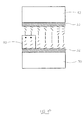
- Figures 4a to 4c offer a possible explanation of how nucleation of the V-state proceeds, for understanding only.
- Figure 4a shows the assumed cell cross-section at zero volts. The majority of the cell is in the H-state. However near the anisotropic protrusion 40 the liquid crystal is held in the twisted state, the state within the protrusion 40 being fixed. At about 1.8V or greater the twist state near to the anisotropic protrusion 40 develops into the V-state as shown in Figure 4b, and then grows to cover the rest of the cell area as shown in Figure 4c.
- a second embodiment of the invention uses tilted anisotropic protrusions to nucleate V-state from H-state
- two indium tin oxide glass coated substrates 30 and 42 were coated, as known to those skilled in the art, with alignment layers 32 and 33 formed from SE610 (Nissan chemicals). Each substrate 30, 42 was then unidirectionally rubbed again as known to those skilled in the art ( Figure 3a). On one of these substrates 30 a mixture of 4:1:15 diacrylate RM257 (Merck) to monoacrylate RM308 (Merck) to toluene was spun at 1200rpm (at 80°C) to form a protrusion layer 34.
- the RM257/RM308 protrusion layer 34 was UV cured through a mask ( Figure 3b) and then rinsed in toluene to leave one substrate 30 coated with about 2.5 micron high tilted anisotropic protrusions 40 ( Figure 3c).
- This substrate 30 was then fabricated into a 5-micron thick pi-cell using the other substrate 42 as shown in Figure 3d. On application of 1.8 volts and greater the V-state was seen to grow out from the areas of anisotropic protrusion to cover the remainder of the display.
- the protrusion height is substantially 50% of the cell gap, being the thickness of the liquid crystal.
- the protrusions may have a height of less than or greater than this, but that the protrusion height should be typically greater than 10% of the cell gap.
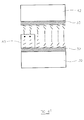
- Figures 5a to 5c offer a potential explanation at how nucleation of the V-state proceeds, for understanding only.
- Figure 5a shows the assumed cell-cross section at zero volts. The majority of the cell is in the H-state. However near the anisotropic protrusion 40 the liquid crystal is held in the V or T state. At about 1.8V and greater the V state near to the anisotropic protrusion 40 begins to grow (Figure 5b) and then grows to cover the rest of the cell area ( Figure 5c).
- the fabricated anisotropic protrusions 40 do not have a rectangular cross-section but a more trapezoidal, triangular or mitre-shaped cross-section depending upon exact processing conditions.
- a third embodiment of the invention uses twisted and tilted anisotropic protrusions to nucleate V-state from H-state. This is the same as the second embodiment with the addition of a small percentage of chiral dopant into the di-functional/mono-functional RM mixture.
- a fourth embodiment of the invention uses tilted anisotropic protrusions for isolation of states in a BTN Device.
- tilted anisotropic protrusions also act as isolation regions in BTN devices. In this case each pixel of a display panel is fully surrounded by such a protrusion
- a fifth embodiment of the invention uses twisted anisotropic protrusions for isolation of states in a BTN Device.
- twisted anisotropic protrusions also act as isolation regions in BTN devices. In this case each pixel of a display panel is fully surrounded by such a protrusion.
- a sixth embodiment of the invention uses tilted and twisted anisotropic protrusions for isolation of states in a BTN Device.
- tilted and twisted anisotropic protrusions also act as isolation regions in BTN devices. In this case each pixel of a display panel is fully surrounded by such a protrusion.
- the positioning of the protrusions depends on whether the protrusions are intended to nucleate, to isolate or both, as described below.
- the protrusion For nucleation, the protrusion need not surround a pixel. However it is preferably present in each pixel to guarantee nucleation within each pixel. Also, each protrusion should partially overlap with the active region of the pixel, or be located adjacent or close to the active region, in order for the applied field to be able to grow the desired state into the active region. For nucleation, the protrusion must be close enough to the active region to experience sufficient influence from any applied field. If aperture ratio and contrast ratios are not paramount the protrusions could be located totally within the active region.
- the protrusion needs to surround each pixel in order to prevent the undesired state growing into it.
- the protrusion need not be within the active region (it could be located in the inter-pixel gap) as isolation does not require a field and hence maximise the aperture ratio and contrast.
- the protrusion should both surround each pixel (for isolation) and overlap partially with, or lie adjacent or close to the active area to allow the field to grow the desired state.
- a black mask may be used to mask off the protrusion.
- isolation and nucleation can be applied to the pi-cell, SBD, BTN, reverse twist TN and other such devices.
Landscapes
- Physics & Mathematics (AREA)
- Nonlinear Science (AREA)
- Chemical & Material Sciences (AREA)
- Crystallography & Structural Chemistry (AREA)
- General Physics & Mathematics (AREA)
- Optics & Photonics (AREA)
- Liquid Crystal (AREA)
Applications Claiming Priority (2)
| Application Number | Priority Date | Filing Date | Title |
|---|---|---|---|
| GB0105434 | 2001-03-06 | ||
| GB0105434A GB2373062A (en) | 2001-03-06 | 2001-03-06 | Nematic Liquid Crystal Devices |
Publications (3)
| Publication Number | Publication Date |
|---|---|
| EP1248142A2 true EP1248142A2 (de) | 2002-10-09 |
| EP1248142A3 EP1248142A3 (de) | 2003-11-05 |
| EP1248142B1 EP1248142B1 (de) | 2007-04-04 |
Family
ID=9910022
Family Applications (1)
| Application Number | Title | Priority Date | Filing Date |
|---|---|---|---|
| EP02250944A Expired - Lifetime EP1248142B1 (de) | 2001-03-06 | 2002-02-12 | Nematische Flüssigkristallvorrichtung und Verfahren zu ihrer Herstellung |
Country Status (7)
| Country | Link |
|---|---|
| US (1) | US7259818B2 (de) |
| EP (1) | EP1248142B1 (de) |
| JP (1) | JP4107562B2 (de) |
| KR (1) | KR20020071766A (de) |
| DE (1) | DE60219232T2 (de) |
| GB (1) | GB2373062A (de) |
| TW (1) | TWI228185B (de) |
Cited By (1)
| Publication number | Priority date | Publication date | Assignee | Title |
|---|---|---|---|---|
| EP1484633A1 (de) * | 2003-06-06 | 2004-12-08 | Seiko Epson Corporation | Flüssigkristallanzeige-Vorrichtung, ihr Herstellungsverfahren und elektronisches Gerät |
Families Citing this family (6)
| Publication number | Priority date | Publication date | Assignee | Title |
|---|---|---|---|---|
| DE60034869T2 (de) * | 2000-03-27 | 2008-02-14 | Hewlett-Packard Co. (N.D.Ges.D.Staates Delaware), Palo Alto | Bistabile nematische Flüssigkristallvorrichtung |
| US7125469B2 (en) * | 2003-10-16 | 2006-10-24 | The Procter & Gamble Company | Temporary wet strength resins |
| JP2005215115A (ja) * | 2004-01-28 | 2005-08-11 | Fujitsu Display Technologies Corp | 液晶表示装置 |
| US7259218B2 (en) * | 2005-02-17 | 2007-08-21 | The Procter + Gamble Company | Processes for making temporary wet strength additives |
| TWI281063B (en) * | 2005-08-16 | 2007-05-11 | Chi Mei Optoelectronics Corp | Liquid crystal display panel and manufacturing method for the same |
| TWI400536B (zh) * | 2008-11-21 | 2013-07-01 | Taiwan Tft Lcd Ass | 光學補償雙折射液晶面板之製作與驅動方法 |
Family Cites Families (20)
| Publication number | Priority date | Publication date | Assignee | Title |
|---|---|---|---|---|
| JPS542580B2 (de) * | 1974-07-01 | 1979-02-09 | ||
| JPS58122516A (ja) * | 1982-01-11 | 1983-07-21 | Kawaguchiko Seimitsu Kk | 液晶カラ−表示体 |
| JPH07120764A (ja) | 1993-09-02 | 1995-05-12 | Matsushita Electric Ind Co Ltd | 液晶表示パネル及びその製造方法 |
| KR100236256B1 (ko) | 1995-04-24 | 1999-12-15 | 가네꼬 히사시 | 액정 표시 장치, 그 제조 방법 및 그 구동 방법 |
| GB9521106D0 (en) * | 1995-10-16 | 1995-12-20 | Secr Defence | Bistable nematic liquid crystal device |
| KR100208970B1 (ko) * | 1995-12-29 | 1999-07-15 | 구자홍 | 액정셀 및 그의 제조방법 |
| GB9615817D0 (en) * | 1996-07-26 | 1996-09-04 | Secr Defence | Liquid crystal device with greyscale |
| GB9704623D0 (en) * | 1997-03-06 | 1997-04-23 | Sharp Kk | Liquid crytal optical element and liquid crystal device incorporating same |
| GB2325530A (en) | 1997-05-22 | 1998-11-25 | Sharp Kk | Liquid crystal device |
| WO1999017153A1 (en) | 1997-10-01 | 1999-04-08 | Matsushita Electric Industrial Co., Ltd. | Liquid crystal alignment film and method of producing the same, and liquid crystal display using the same and method of producing the same |
| KR20010042407A (ko) * | 1998-04-08 | 2001-05-25 | 모리시타 요이찌 | 패럴렐배향 액정표시소자 및 그 제조방법, 그리고스플레이-벤드 전이시간의 평가법 및 그 평가장치 |
| JP3347678B2 (ja) * | 1998-06-18 | 2002-11-20 | キヤノン株式会社 | 液晶素子とその駆動方法 |
| US6879364B1 (en) * | 1998-09-18 | 2005-04-12 | Fujitsu Display Technologies Corporation | Liquid crystal display apparatus having alignment control for brightness and response |
| GB2343011A (en) * | 1998-10-20 | 2000-04-26 | Sharp Kk | A liquid crystal display device |
| WO2001023951A1 (en) | 1999-09-30 | 2001-04-05 | Technology Resource International Corporation | Multi-domain liquid crystal cell |
| US6671019B1 (en) | 1999-11-12 | 2003-12-30 | Case Western Reserve University | Electrode patterns for liquid crystal cells |
| GB2356462A (en) * | 1999-11-16 | 2001-05-23 | Sharp Kk | Optical properties of spacers in liquid crystal devices |
| JP3910370B2 (ja) | 2000-02-08 | 2007-04-25 | シャープ株式会社 | 液晶表示デバイス |
| DE60034869T2 (de) * | 2000-03-27 | 2008-02-14 | Hewlett-Packard Co. (N.D.Ges.D.Staates Delaware), Palo Alto | Bistabile nematische Flüssigkristallvorrichtung |
| US6897918B1 (en) * | 2000-09-15 | 2005-05-24 | Toray Industries, Inc. | Color filter with protrusion |
-
2001
- 2001-03-06 GB GB0105434A patent/GB2373062A/en not_active Withdrawn
-
2002
- 2002-02-12 EP EP02250944A patent/EP1248142B1/de not_active Expired - Lifetime
- 2002-02-12 DE DE60219232T patent/DE60219232T2/de not_active Expired - Lifetime
- 2002-02-26 JP JP2002050164A patent/JP4107562B2/ja not_active Expired - Fee Related
- 2002-03-01 US US10/087,660 patent/US7259818B2/en not_active Expired - Lifetime
- 2002-03-05 TW TW091104055A patent/TWI228185B/zh not_active IP Right Cessation
- 2002-03-06 KR KR1020020011897A patent/KR20020071766A/ko not_active Ceased
Cited By (2)
| Publication number | Priority date | Publication date | Assignee | Title |
|---|---|---|---|---|
| EP1484633A1 (de) * | 2003-06-06 | 2004-12-08 | Seiko Epson Corporation | Flüssigkristallanzeige-Vorrichtung, ihr Herstellungsverfahren und elektronisches Gerät |
| US7139052B2 (en) | 2003-06-06 | 2006-11-21 | Seiko Epson Corporation | Liquid crystal display device, method of manufacturing the same, and electronic apparatus |
Also Published As
| Publication number | Publication date |
|---|---|
| US20020126245A1 (en) | 2002-09-12 |
| EP1248142A3 (de) | 2003-11-05 |
| KR20020071766A (ko) | 2002-09-13 |
| DE60219232D1 (de) | 2007-05-16 |
| EP1248142B1 (de) | 2007-04-04 |
| JP2002311436A (ja) | 2002-10-23 |
| JP4107562B2 (ja) | 2008-06-25 |
| GB2373062A (en) | 2002-09-11 |
| GB0105434D0 (en) | 2001-04-25 |
| DE60219232T2 (de) | 2008-01-03 |
| TWI228185B (en) | 2005-02-21 |
| US7259818B2 (en) | 2007-08-21 |
Similar Documents
| Publication | Publication Date | Title |
|---|---|---|
| JP3338025B2 (ja) | 液晶表示素子 | |
| US6714276B2 (en) | Liquid crystal display device | |
| US6774967B2 (en) | Multi-domain liquid crystal display device | |
| US6512569B1 (en) | Liquid crystal display device and a method of manufacture thereof, and a substrate and a method of manufacture thereof | |
| US6201592B1 (en) | Liquid crystal display device and method for producing the same | |
| US6930739B2 (en) | Liquid crystal device | |
| US7379137B2 (en) | Liquid crystal display device | |
| JP4817589B2 (ja) | ネマチック液晶電気光学要素及びデバイス | |
| JPH06294959A (ja) | 液晶表示装置とその製造方法 | |
| US5877831A (en) | Multi-domain LCD with subpixels having twist angles with opposite twist sense of within 60 and small/greater 90 degrees | |
| JP3144329B2 (ja) | 液晶表示素子 | |
| US7259818B2 (en) | Nematic liquid crystal devices comprising surface protrusions formed of anisotropic material for nucleation of an active region | |
| JP4203943B2 (ja) | 液晶表示デバイス | |
| US20070013849A1 (en) | Multi-domain vertical alignment liquid crystal display | |
| JP4030362B2 (ja) | 液晶表示装置 | |
| JP4737913B2 (ja) | 液晶表示素子及び液晶表示素子の駆動方法 | |
| US6600537B2 (en) | Liquid crystal device | |
| KR100725218B1 (ko) | 듀얼모드 액정표시장치 및 그의 구동방법 | |
| US7307678B2 (en) | Liquid crystal display and fabricating method thereof | |
| JP2001235750A (ja) | 液晶表示装置 | |
| US20030067567A1 (en) | Ferroelectric liquid crystal display and driving method thereof | |
| Towler | Future LC Technologies | |
| JP2000275684A (ja) | 液晶素子およびそれを用いた液晶装置 | |
| JP2004078099A (ja) | 液晶素子の製造方法 | |
| GB2359142A (en) | A liquid crystal display device |
Legal Events
| Date | Code | Title | Description |
|---|---|---|---|
| PUAI | Public reference made under article 153(3) epc to a published international application that has entered the european phase |
Free format text: ORIGINAL CODE: 0009012 |
|
| AK | Designated contracting states |
Kind code of ref document: A2 Designated state(s): AT BE CH CY DE DK ES FI FR GB GR IE IT LI LU MC NL PT SE TR |
|
| AX | Request for extension of the european patent |
Free format text: AL;LT;LV;MK;RO;SI |
|
| PUAL | Search report despatched |
Free format text: ORIGINAL CODE: 0009013 |
|
| RIC1 | Information provided on ipc code assigned before grant |
Ipc: 7G 02F 1/139 A Ipc: 7G 02F 1/1337 B |
|
| AK | Designated contracting states |
Kind code of ref document: A3 Designated state(s): AT BE CH CY DE DK ES FI FR GB GR IE IT LI LU MC NL PT SE TR |
|
| AX | Request for extension of the european patent |
Extension state: AL LT LV MK RO SI |
|
| 17P | Request for examination filed |
Effective date: 20040430 |
|
| AKX | Designation fees paid |
Designated state(s): DE FR GB |
|
| 17Q | First examination report despatched |
Effective date: 20040923 |
|
| GRAP | Despatch of communication of intention to grant a patent |
Free format text: ORIGINAL CODE: EPIDOSNIGR1 |
|
| RTI1 | Title (correction) |
Free format text: NEMATIC LIQUID CRYSTAL DEVICE, AND METHOD OF PRODUCTION THEREOF |
|
| GRAS | Grant fee paid |
Free format text: ORIGINAL CODE: EPIDOSNIGR3 |
|
| GRAA | (expected) grant |
Free format text: ORIGINAL CODE: 0009210 |
|
| AK | Designated contracting states |
Kind code of ref document: B1 Designated state(s): DE FR GB |
|
| REG | Reference to a national code |
Ref country code: GB Ref legal event code: FG4D |
|
| REF | Corresponds to: |
Ref document number: 60219232 Country of ref document: DE Date of ref document: 20070516 Kind code of ref document: P |
|
| PLBE | No opposition filed within time limit |
Free format text: ORIGINAL CODE: 0009261 |
|
| STAA | Information on the status of an ep patent application or granted ep patent |
Free format text: STATUS: NO OPPOSITION FILED WITHIN TIME LIMIT |
|
| 26N | No opposition filed |
Effective date: 20080107 |
|
| PGFP | Annual fee paid to national office [announced via postgrant information from national office to epo] |
Ref country code: FR Payment date: 20130301 Year of fee payment: 12 Ref country code: GB Payment date: 20130207 Year of fee payment: 12 |
|
| GBPC | Gb: european patent ceased through non-payment of renewal fee |
Effective date: 20140212 |
|
| REG | Reference to a national code |
Ref country code: FR Ref legal event code: ST Effective date: 20141031 |
|
| PG25 | Lapsed in a contracting state [announced via postgrant information from national office to epo] |
Ref country code: FR Free format text: LAPSE BECAUSE OF NON-PAYMENT OF DUE FEES Effective date: 20140228 Ref country code: GB Free format text: LAPSE BECAUSE OF NON-PAYMENT OF DUE FEES Effective date: 20140212 |
|
| PGFP | Annual fee paid to national office [announced via postgrant information from national office to epo] |
Ref country code: DE Payment date: 20160218 Year of fee payment: 15 |
|
| REG | Reference to a national code |
Ref country code: DE Ref legal event code: R119 Ref document number: 60219232 Country of ref document: DE |
|
| PG25 | Lapsed in a contracting state [announced via postgrant information from national office to epo] |
Ref country code: DE Free format text: LAPSE BECAUSE OF NON-PAYMENT OF DUE FEES Effective date: 20170901 |