EP1247089B1 - Kohlenstoff-nano-röhrchen-vorrichtung - Google Patents
Kohlenstoff-nano-röhrchen-vorrichtung Download PDFInfo
- Publication number
- EP1247089B1 EP1247089B1 EP00992511A EP00992511A EP1247089B1 EP 1247089 B1 EP1247089 B1 EP 1247089B1 EP 00992511 A EP00992511 A EP 00992511A EP 00992511 A EP00992511 A EP 00992511A EP 1247089 B1 EP1247089 B1 EP 1247089B1
- Authority
- EP
- European Patent Office
- Prior art keywords
- nanotube
- molecular sensor
- gold
- molecular
- catalyst
- Prior art date
- Legal status (The legal status is an assumption and is not a legal conclusion. Google has not performed a legal analysis and makes no representation as to the accuracy of the status listed.)
- Expired - Lifetime
Links
Images


Classifications
-
- G—PHYSICS
- G01—MEASURING; TESTING
- G01N—INVESTIGATING OR ANALYSING MATERIALS BY DETERMINING THEIR CHEMICAL OR PHYSICAL PROPERTIES
- G01N27/00—Investigating or analysing materials by the use of electric, electrochemical, or magnetic means
- G01N27/02—Investigating or analysing materials by the use of electric, electrochemical, or magnetic means by investigating impedance
- G01N27/04—Investigating or analysing materials by the use of electric, electrochemical, or magnetic means by investigating impedance by investigating resistance
- G01N27/12—Investigating or analysing materials by the use of electric, electrochemical, or magnetic means by investigating impedance by investigating resistance of a solid body in dependence upon absorption of a fluid; of a solid body in dependence upon reaction with a fluid, for detecting components in the fluid
- G01N27/125—Composition of the body, e.g. the composition of its sensitive layer
- G01N27/127—Composition of the body, e.g. the composition of its sensitive layer comprising nanoparticles
-
- B—PERFORMING OPERATIONS; TRANSPORTING
- B82—NANOTECHNOLOGY
- B82Y—SPECIFIC USES OR APPLICATIONS OF NANOSTRUCTURES; MEASUREMENT OR ANALYSIS OF NANOSTRUCTURES; MANUFACTURE OR TREATMENT OF NANOSTRUCTURES
- B82Y15/00—Nanotechnology for interacting, sensing or actuating, e.g. quantum dots as markers in protein assays or molecular motors
-
- B—PERFORMING OPERATIONS; TRANSPORTING
- B82—NANOTECHNOLOGY
- B82Y—SPECIFIC USES OR APPLICATIONS OF NANOSTRUCTURES; MEASUREMENT OR ANALYSIS OF NANOSTRUCTURES; MANUFACTURE OR TREATMENT OF NANOSTRUCTURES
- B82Y30/00—Nanotechnology for materials or surface science, e.g. nanocomposites
Definitions
- This invention relates generally to nanotube devices. More particularly, it relates to a new class of nanotube chemical and biological sensors.
- Sensing chemical and biological species plays an important role in many industrial, agricultural, medical, and environmental processes. Detection of NO 2 gas, for example, provides a crucial measure of environmental pollution due to combustion or automotive emissions. The amount of NH 3 also needs to be closely monitored in industrial, medical and living environments. Moreover, there is a growing need to detect biological species in a variety of biomedical applications.
- Chemical sensors in the prior art commonly employ solid state materials, such as semiconducting metal oxides, as sensing agents.
- the sensing is achieved by detecting change in electrical resistance of the sensor resulted from adsorption of foreign chemical species onto the sensing material.
- sensors of this type In order to achieve significant sensitivity, however, sensors of this type must operate at elevated temperatures so to enhance chemical reactivity.
- Other drawbacks of these prior art sensors include long recovery times (if not rendering irreversibility), poor reproducibility, and very limited range of chemical species each sensor is able to detect.
- the present invention comprises a molecular sensor comprising: a) a nanotube device comprising at least one carbon nanotube, wherein a first end of said nanotube is in electrical contact with a first conducting element and a second end of said nanotube is in electrical contact with a second conducting element; and b) a coating of one or more sensing agents deposited on said nanotube; wherein said sensing agents are so chosen such that the agents-coated nanotube responds to a particular molecular species.
- the sensing agents may comprise one or more materials selected from the group consisting of metal particles, polymers, and biological species, and preferably including gold, platinum, nickel, rhodium, palladium, TiO 2 , thiol, and enzymes.
- the nanotube may be semiconducting.
- the molecular sensor may further comprise a voltage source applying a gating voltage to said nanotube, wherein said gating voltage is so chosen such that said nanotube, biased with said gating voltage, responds to a particular molecular species.
- the gating voltage may be in the range of-20 to 20 Volts.
- the at least one nanotube may be a single-walled nanotube.
- At least one of said conducting elements may comprise an island of a catalyst material covered by a metal electrode, and at least one of said ends of said nanotube may be rooted in said catalyst island and covered by said metal electrode.
- the metal electrode may comprise an alloy of nickel-gold or titanium-gold.
- the catalyst material may be selected from a groups consisting of iron, molybdenum, cobalt, nickel, ruthenium, zinc and oxides thereof or may comprise Fe 2 O 3 and alumina nanoparticles.
- the catalyst island may be in the range of 3-5 microns in size.
- At least one of said conducting elements may comprise a metal pad (33) covering at least one of said ends of said nanotube, and said metal pad may comprise a material selected from the group consisting of titanium, gold, aluminium, chromium, and platinum.
- the nanotube devices of the present invention demonstrate high sensitivity, robust response, and a tunable selectivity to a wide range of molecular species. They operate in gaseous and liquid environments.
- FIGS. 1A-1C illustrate a method for synthesizing individually distinct nanotubes on a silicon substrate that is patterned with catalyst islands.
- the principle procedures of the method have been reported in the art by the inventors ( Nature 395,878 (1998 )).
- a layer of resist 10 is disposed and patterned on a top surface of a substrate 11, as illustrated in FIG. 1A .
- the substrate 11 is made of doped silicon with a layer of native oxide. Patterning on the resist 10 is typically performed by electron-beam lithography, producing holes 12 that expose the underlying substrate 11.
- the holes 12 are typically 5 microns in size, spaced at a distance of 10 microns apart.
- a few drops of a catalyst material are placed on the surface of the substrate 11, filling the holes 12.
- the catalyst preparation includes mixing 15mg of alumina nanoparticles, 0.05 mmol of Fe(NO 3 ) 3 9H 2 O, and 0.015 mmol of MoO 2 (acac) 2 in 15ml
- FIG. 1B shows an array of isolated catalyst islands 13 on the substrate 11, as shown in FIG. 1B .
- the catalyst- patterned substrate is then heated in a tube furnace to above 900°C while exposed to a flow of methane. Heating decomposes Fe(NO 3 ) 3 to Fe 2 O 3 .
- the Fe 2 O 3 /nanoparticles mixture is capable of catalyzing the growth of carbon nanotubes when exposed to methane gas at elevated temperatures.
- the carbon nanotubes thus grown are predominantly individually distinct, single- walled nanotubes with few structural defects.
- FIG. 1C shows these nanotubes 14 emanated from the catalyst islands 13 on the substrate 11.
- nanotubes are found to be substantially straight, typically extending up to more than 10 microns in length with diameters ranging from 1-3 nanometers. Moreover, a number of the nanotubes are bridging adjacent islands. A nanotube bridge forms when a tube growing from one catalyst island falls on and interacts with another island during the synthesis process as described.
- the substrate can be made of a material selected from a group consisting of silicon, alumina, quartz, silica and silicon nitride.
- the catalyst islands comprise a material selected from a group including iron, molybdenum, cobalt, nickel, ruthenium, zinc and oxides thereof.
- the nanotubes can be semiconducting, or metallic.
- nanotubes made of other materials can also be grown by following a synthesis process similar to what is described above. Those skilled in the art will be able to implement the corresponding synthesis procedures.
- the nanotube chip thus produced can be incorporated into a variety of electronic and mechanical devices.
- a device comprising a single nanotube can also be readily made.
- AFM atomic force microscopy
- the nanotubes bridging two catalyst islands are cut mechanically or electrically until a single tube remains.
- Electron-beam lithography is then employed to deposit metal electrodes onto the two catalyst islands bridged by the nanotube.
- the electrodes are typically made of an alloy of nickel-gold, or titanium-gold. For example, they can be 20 nanometers of nickel with 60 nanometers gold on top. These electrodes provide electrical connections between the nanotube and macroscopic electronic circuits.
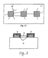
- FIG. 2 shows an exemplary embodiment of a nanotube device comprising a single nanotube 20 disposed between two catalyst islands 21 on a substrate 22.
- Two metal electrodes 23 are made to fully cover respective catalyst islands 21, including the two ends 24 of the bridging nanotube 20.
- FIGS. 3A-3B show a method for synthesizing a film of nanotubes on a substrate that is initially covered with a layer of catalyst.
- a quartz substrate 30 is coated with a layer of catalyst 31 by spin-coating, as shown in FIG. 3A .
- the catalyst is typically prepared by mixing 15mg of alumina nanoparticles, 0.05 mmol of Fe (NO 3 ) 3 9H 2 O, and 0.015 mmol of MoO 2 (acac) 2 in 15 ml of methanol.
- the catalyst-covered substrate is then heated to above 900°C in a flow of methane, yielding a film of interconnected single-walled carbon nanotubes 32 on the substrate, as shown in FIG. 3B .
- Two metal electrodes 33 each comprising 20 nanometers of titanium followed by 60 nanometre of gold, are then evaporated onto the nanotube film through a shadow mask, such that there is a metal-free gap forming between the two electrodes 33.
- Such a nanotube film device can be easily produced in a scaled-up fashion with low cost.
- the substrate in FIGS. 3A-3B is typically made of a material selected from a group consisting of silicon, alumina, quartz, silica and silicon nitride.
- the catalyst islands comprise a material selected from a group including iron, molybdenum, cobalt, nickel, ruthenium, zinc and oxides thereof.
- the nanotubes can be semiconducting, or metallic.
- the electrodes is typically made of an alloy of nickel-gold, or titanium-gold.
- the nanotube devices described above can be further physically or chemically modified, so as to be tailored for a particular application.
- a semiconducting or metallic carbon nanotube exhibits inherent change in electrical conductance when exposed to certain chemical gases, resulted from adsorption of the gas particles on the nanotube. More significantly, by depositing one or more sensing agents onto the nanotube, its sensitivity to a wide range of chemical and biological species can be achieved. The selectivity of the nanotube to chemical species can be also tuned by applying a gating voltage to the nanotube.
- the gating voltage effectively shifts the Fermi energy level of the nanotube, enabling the nanotube to be more responsive to a particular species.
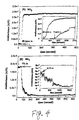
- FIG. 4 displays electrical responses of a device comprising a semiconducting single-walled carbon nanotube to various amounts of NO 2 and NH 3 gas, respectively.
- the gas sensing is carried out by enclosing the device in a glass flask.
- the flask is equipped with electrical feedthrough that makes electrical connections between the device and the electrical measurement circuits on the outside. It also permits a flow of gas.
- a carrier gas e. g., Ar or air
- diluted with NO 2 or NH 3 then flows through the flask, while the electrical response of the nanotube is recorded.
- the device displays fast and significant response to the arrival of NO 2 and NH 3 , respectively.
- the electrical characteristics of the nanotube is able to fully recover in a flow of pure carrier gas over a period of several hours.
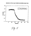
- FIG. 5 shows electrical response of a gold-decorated single nanotube to thiol vapor.
- Gold is deposited on the nanotube by evaporation. Since it does not wet carbon, the evaporated gold particles decorate, rather than forming a continuous layer on the nanotube.
- the observed response to thiol results from the presence of the gold particles in this case, since the carbon nanotube alone does not respond to thiol. Given that many biological molecules like to link themselves onto thiol, by attaching a layer of thiol to a gold-decorated nanotube, this composite system promises to be a versatile biological sensor.
- FIG. 6 shows electrical responses of an as-grown nanotube film (mat) device and a PMMA(polymethylmethacrylate)-covered nanotube film (mat) device to NO 2 gas.
- the PMMA coating in the later case is typically about 100 nanometers thick, and its presence significantly improves the sensitivity and the response time of the nanotube device to NO 2 .
- FIG. 7A displays electrical response of a gold-decorated nanotube film device to thiol vapor
- FIG. 7B shows the detection of avidin (a protein) using a thiol-coated-gold-decorated film device.
- avidin a protein
- FIG. 7B shows the detection of avidin (a protein) using a thiol-coated-gold-decorated film device.
- gold particles are first evaporated onto the nanotube film, followed by attaching a monolayer of thiol with carboxylic functional group to the gold particles.
- the presence of thiol modifies the electrical conductance of the nanotube device.
- the carboxylic groups of the thiol molecules like to be linked to avidin molecules via carbodimide chemistry, giving rise to further change in electrical conductance of the nanotube film device.
- the nanotube device operates in a liquid environment.
- FIG. 8 shows the detection of H 2 using a platinum-modified nanotube film device. Platinum particles are deposited onto and decorate the nanotubes film. It is their presence that enables the device to respond to H 2 molecules.
- the corresponding enzyme-coated nanotube device displays changes in its electrical conductance when exposed to glucose, and other biological species. This would have important implications in medicine. Sensing CO has also been achieved by using modified nanotube devices.
- sensing agents e.g., nickel, rhodium, palladium, TiO 2
- polymers e.g., polymers, and biological species
- the capabilities of the nanotube devices of the present invention as chemical and biological sensors are not merely limited to the exemplary embodiments described above.
- the nanotube devices of the present invention can be utilized as electrochemical, electromechanical and other functional devices.
Claims (12)
- Molekularer Sensor, umfassend:a) eine Nanoröhren-Vorrichtung, die wenigstens eine Kohlenstoffnanoröhre (20) umfasst, wobei ein erstes Ende der Nanoröhre (20) mit einem ersten leitenden Element in elektrischem Kontakt ist und ein zweites Ende der Nanoröhre (20) mit einem zweiten leitenden Element in elektrischem Kontakt ist; undb) eine auf der Nanoröhre (20) aufgebrachte Beschichtung aus einem oder mehreren Sensorstoffen, wobei die Sensorstoffe so gewählt sind, dass die stoffbeschichtete Nanoröhre (20) auf eine bestimmte molekulare Spezies anspricht.
- Molekularer Sensor nach Anspruch 1, wobei der eine oder die mehreren Sensorstoffe eine oder mehrere Substanzen umfassen, die aus der der Gruppe bestehend aus Metallpartikeln, Polymeren und biologischen Spezies ausgewählt sind, wobei diese Gruppe vorzugsweise Gold, Platin, Nickel, Rhodium, Palladium, TiO2, Thiol und Enzyme einschließt.
- Molekularer Sensor nach entweder Anspruch 1 oder Anspruch 2, wobei die Nanoröhre (20) halbleitend ist.
- Molekularer Sensor nach einem der Ansprüche 1 bis 3, der außerdem eine Spannungsquelle umfasst, die eine Gate-Spannung an die Nanoröhre (20) anlegt, wobei die Gate-Spannung so gewählt ist, dass die mit dieser Gate-Spannung vorgespannte Nanoröhre (20) auf eine bestimmte molekulare Spezies anspricht.
- Molekularer Sensor nach Anspruch 4, wobei die Gate-Spannung im Bereich von -20 bis 20 Volt liegt.
- Molekularer Sensor nach einem der Ansprüche 1 bis 5, wobei die wenigstens eine Nanoröhre (20) eine einwandige Nanoröhre ist.
- Molekularer Sensor nach einem der Ansprüche 1 bis 6, wobei wenigstens eines der leitenden Elemente eine Insel (21) aus einem Katalysatormaterial umfasst, die von einer Metallelektrode (23) bedeckt wird, und wobei wenigstens eines der Enden der Nanoröhre (20) in der Katalysatorinsel (21) verwurzelt ist und von der Metallelektrode (23) bedeckt wird.
- Molekularer Sensor nach Anspruch 7, wobei die Metallelektrode (23) eine Nickel-Gold- oder Titan-Gold-Legierung umfasst.
- Molekularer Sensor nach entweder Anspruch 7 oder Anspruch 8, wobei das Katalysatormaterial aus einer Gruppe bestehend aus Eisen, Molybdän, Cobalt, Nickel, Ruthenium, Zink und deren Oxiden ausgewählt ist.
- Molekularer Sensor nach entweder Anspruch 7 oder Anspruch 8, wobei das Katalysatormaterial Fe2O3 und Aluminiumoxid-Nanopartikel umfasst.
- Molekularer Sensor nach einem der Ansprüche 7 bis 10, wobei die Katalysatorinsel (21) in der Größe im Bereich von 3-5 Mikrometern liegt.
- Molekularer Sensor nach einem der Ansprüche 1 bis 6, wobei wenigstens eines der leitenden Elemente eine Metall-Kontaktierungsstelle (33) umfasst, die wenigstens eines der Enden der Nanoröhre (20) bedeckt, und die Metall-Kontaktierungsstelle (33) ein Material umfasst, das aus der Gruppe bestehend aus Titan, Gold, Aluminium, Chrom und Platin ausgewählt ist.
Applications Claiming Priority (3)
| Application Number | Priority Date | Filing Date | Title |
|---|---|---|---|
| US17120099P | 1999-12-15 | 1999-12-15 | |
| US171200P | 1999-12-15 | ||
| PCT/US2000/042186 WO2001044796A1 (en) | 1999-12-15 | 2000-11-15 | Carbon nanotube devices |
Publications (3)
| Publication Number | Publication Date |
|---|---|
| EP1247089A1 EP1247089A1 (de) | 2002-10-09 |
| EP1247089A4 EP1247089A4 (de) | 2003-05-07 |
| EP1247089B1 true EP1247089B1 (de) | 2008-07-23 |
Family
ID=22622902
Family Applications (1)
| Application Number | Title | Priority Date | Filing Date |
|---|---|---|---|
| EP00992511A Expired - Lifetime EP1247089B1 (de) | 1999-12-15 | 2000-11-15 | Kohlenstoff-nano-röhrchen-vorrichtung |
Country Status (5)
| Country | Link |
|---|---|
| EP (1) | EP1247089B1 (de) |
| JP (1) | JP2003517604A (de) |
| AT (1) | ATE402407T1 (de) |
| DE (1) | DE60039632D1 (de) |
| WO (1) | WO2001044796A1 (de) |
Families Citing this family (95)
| Publication number | Priority date | Publication date | Assignee | Title |
|---|---|---|---|---|
| AU2002324426B2 (en) * | 2000-08-22 | 2007-07-26 | President And Fellows Of Harvard College | Nanoscale wires and related devices |
| AU2007211919B2 (en) * | 2000-08-22 | 2009-01-08 | President And Fellows Of Harvard College | Nanoscale wires and related devices |
| EP1736760A3 (de) * | 2000-12-11 | 2008-06-18 | President And Fellows Of Harvard College | Nanosensoren |
| KR20090049095A (ko) | 2000-12-11 | 2009-05-15 | 프레지던트 앤드 펠로우즈 오브 하버드 칼리지 | 나노센서 |
| DE10123876A1 (de) * | 2001-05-16 | 2002-11-28 | Infineon Technologies Ag | Nanoröhren-Anordnung und Verfahren zum Herstellen einer Nanoröhren-Anordnung |
| US7259410B2 (en) | 2001-07-25 | 2007-08-21 | Nantero, Inc. | Devices having horizontally-disposed nanofabric articles and methods of making the same |
| US6835591B2 (en) * | 2001-07-25 | 2004-12-28 | Nantero, Inc. | Methods of nanotube films and articles |
| US6706402B2 (en) * | 2001-07-25 | 2004-03-16 | Nantero, Inc. | Nanotube films and articles |
| US6924538B2 (en) | 2001-07-25 | 2005-08-02 | Nantero, Inc. | Devices having vertically-disposed nanofabric articles and methods of making the same |
| CA2468251A1 (en) * | 2001-11-26 | 2003-06-05 | Sony International (Europe) G.M.B.H. | The use of 1d semiconductor materials as chemical sensing materials, produced and operated close to room temperature |
| US7531136B2 (en) | 2001-11-26 | 2009-05-12 | Sony Deutschland Gmbh | Chemical sensor |
| FR2833935B1 (fr) | 2001-12-26 | 2004-01-30 | Commissariat Energie Atomique | Procede de fabrication d'au moins un nanotube entre deux elements electriquement conducteurs et dispositif pour mettre en oeuvre un tel procede |
| US8152991B2 (en) | 2005-10-27 | 2012-04-10 | Nanomix, Inc. | Ammonia nanosensors, and environmental control system |
| US8154093B2 (en) | 2002-01-16 | 2012-04-10 | Nanomix, Inc. | Nano-electronic sensors for chemical and biological analytes, including capacitance and bio-membrane devices |
| US6894359B2 (en) | 2002-09-04 | 2005-05-17 | Nanomix, Inc. | Sensitivity control for nanotube sensors |
| US7522040B2 (en) | 2004-04-20 | 2009-04-21 | Nanomix, Inc. | Remotely communicating, battery-powered nanostructure sensor devices |
| US7312095B1 (en) | 2002-03-15 | 2007-12-25 | Nanomix, Inc. | Modification of selectivity for sensing for nanostructure sensing device arrays |
| US7547931B2 (en) | 2003-09-05 | 2009-06-16 | Nanomix, Inc. | Nanoelectronic capnometer adaptor including a nanoelectric sensor selectively sensitive to at least one gaseous constituent of exhaled breath |
| US7714398B2 (en) | 2002-09-05 | 2010-05-11 | Nanomix, Inc. | Nanoelectronic measurement system for physiologic gases and improved nanosensor for carbon dioxide |
| WO2003078652A2 (en) | 2002-03-15 | 2003-09-25 | Nanomix, Inc. | Modification of selectivity for sensing for nanostructure device arrays |
| DE10220194A1 (de) * | 2002-05-06 | 2003-11-27 | Infineon Technologies Ag | Kontaktierung von Nanoröhren |
| US7948041B2 (en) | 2005-05-19 | 2011-05-24 | Nanomix, Inc. | Sensor having a thin-film inhibition layer |
| DE10247679A1 (de) * | 2002-10-12 | 2004-04-22 | Fujitsu Ltd., Kawasaki | Halbleitergrundstruktur für Molekularelektronik und Molekularelektronik-basierte Biosensorik |
| AU2003304248A1 (en) | 2002-10-29 | 2005-01-13 | President And Fellows Of Harvard College | Carbon nanotube device fabrication |
| US7253434B2 (en) | 2002-10-29 | 2007-08-07 | President And Fellows Of Harvard College | Suspended carbon nanotube field effect transistor |
| WO2004044586A1 (en) * | 2002-11-08 | 2004-05-27 | Nanomix, Inc. | Nanotube-based electronic detection of biological molecules |
| US6949931B2 (en) | 2002-11-26 | 2005-09-27 | Honeywell International Inc. | Nanotube sensor |
| US6936496B2 (en) | 2002-12-20 | 2005-08-30 | Hewlett-Packard Development Company, L.P. | Nanowire filament |
| US6870361B2 (en) | 2002-12-21 | 2005-03-22 | Agilent Technologies, Inc. | System with nano-scale conductor and nano-opening |
| US7075141B2 (en) | 2003-03-28 | 2006-07-11 | Nantero, Inc. | Four terminal non-volatile transistor device |
| US7113426B2 (en) | 2003-03-28 | 2006-09-26 | Nantero, Inc. | Non-volatile RAM cell and array using nanotube switch position for information state |
| US6944054B2 (en) | 2003-03-28 | 2005-09-13 | Nantero, Inc. | NRAM bit selectable two-device nanotube array |
| US7045421B2 (en) | 2003-04-22 | 2006-05-16 | Nantero, Inc. | Process for making bit selectable devices having elements made with nanotubes |
| US6995046B2 (en) | 2003-04-22 | 2006-02-07 | Nantero, Inc. | Process for making byte erasable devices having elements made with nanotubes |
| WO2005019793A2 (en) | 2003-05-14 | 2005-03-03 | Nantero, Inc. | Sensor platform using a horizontally oriented nanotube element |
| JP4774476B2 (ja) * | 2004-02-16 | 2011-09-14 | 独立行政法人科学技術振興機構 | センサー |
| CN102183569B (zh) * | 2003-05-23 | 2013-09-04 | 独立行政法人科学技术振兴机构 | 试样中的被检测物质的检测方法 |
| WO2005005687A1 (en) * | 2003-07-02 | 2005-01-20 | Seldon Technologies, Llc | Method of coating nanosturctures with metal using metal salts |
| US7750285B2 (en) | 2003-07-18 | 2010-07-06 | Japan Science And Technology Agency | Optical sensor including photoconductive material and carbon nanotube |
| US20050036905A1 (en) * | 2003-08-12 | 2005-02-17 | Matsushita Electric Works, Ltd. | Defect controlled nanotube sensor and method of production |
| CN101562049B (zh) | 2003-08-13 | 2012-09-05 | 南泰若股份有限公司 | 具有多个控件的基于纳米管的开关元件及由其制成的电路 |
| US7115960B2 (en) | 2003-08-13 | 2006-10-03 | Nantero, Inc. | Nanotube-based switching elements |
| WO2005048296A2 (en) | 2003-08-13 | 2005-05-26 | Nantero, Inc. | Nanotube-based switching elements with multiple controls and circuits made from same |
| JP4669213B2 (ja) * | 2003-08-29 | 2011-04-13 | 独立行政法人科学技術振興機構 | 電界効果トランジスタ及び単一電子トランジスタ並びにそれを用いたセンサ |
| EP1664724A4 (de) * | 2003-09-12 | 2007-05-02 | Nanomix Inc | Nanoelektronischer kohlendioxidsensor |
| US7378715B2 (en) * | 2003-10-10 | 2008-05-27 | General Electric Company | Free-standing electrostatically-doped carbon nanotube device |
| US6921684B2 (en) * | 2003-10-17 | 2005-07-26 | Intel Corporation | Method of sorting carbon nanotubes including protecting metallic nanotubes and removing the semiconducting nanotubes |
| JP4238715B2 (ja) * | 2003-12-15 | 2009-03-18 | 富士ゼロックス株式会社 | 電気化学測定用電極 |
| US7208094B2 (en) | 2003-12-17 | 2007-04-24 | Hewlett-Packard Development Company, L.P. | Methods of bridging lateral nanowires and device using same |
| US8048377B1 (en) * | 2004-03-08 | 2011-11-01 | Hewlett-Packard Development Company, L.P. | Immobilizing chemical or biological sensing molecules on semi-conducting nanowires |
| WO2006071895A2 (en) * | 2004-12-28 | 2006-07-06 | Nanomix, Inc. | Nanoelectronic devices for dna detection, and recognition of polynucleotide sequences |
| US7652342B2 (en) | 2004-06-18 | 2010-01-26 | Nantero, Inc. | Nanotube-based transfer devices and related circuits |
| US7161403B2 (en) | 2004-06-18 | 2007-01-09 | Nantero, Inc. | Storage elements using nanotube switching elements |
| US7329931B2 (en) | 2004-06-18 | 2008-02-12 | Nantero, Inc. | Receiver circuit using nanotube-based switches and transistors |
| US7330709B2 (en) | 2004-06-18 | 2008-02-12 | Nantero, Inc. | Receiver circuit using nanotube-based switches and logic |
| US7164744B2 (en) | 2004-06-18 | 2007-01-16 | Nantero, Inc. | Nanotube-based logic driver circuits |
| WO2007013872A2 (en) | 2004-07-22 | 2007-02-01 | The Board Of Trustees Of The University Of Illinois | Sensors employing single-walled carbon nanotubes |
| WO2006024023A2 (en) * | 2004-08-24 | 2006-03-02 | Nanomix, Inc. | Nanotube sensor devices for dna detection |
| US7226818B2 (en) | 2004-10-15 | 2007-06-05 | General Electric Company | High performance field effect transistors comprising carbon nanotubes fabricated using solution based processing |
| JP5048213B2 (ja) * | 2004-12-07 | 2012-10-17 | 国立大学法人大阪大学 | 半導体式ガス検知素子 |
| WO2007084163A2 (en) | 2005-04-06 | 2007-07-26 | President And Fellows Of Harvard College | Molecular characterization with carbon nanotube control |
| US20100227382A1 (en) | 2005-05-25 | 2010-09-09 | President And Fellows Of Harvard College | Nanoscale sensors |
| JP4825968B2 (ja) * | 2005-05-26 | 2011-11-30 | 国立大学法人九州大学 | カーボンナノチューブセンサ及びその製造方法 |
| US7645482B2 (en) * | 2005-08-04 | 2010-01-12 | The Regents Of The University Of California | Method to make and use long single-walled carbon nanotubes as electrical conductors |
| US7718224B2 (en) * | 2005-08-04 | 2010-05-18 | The Regents Of The University Of California | Synthesis of single-walled carbon nanotubes |
| US8240190B2 (en) | 2005-08-23 | 2012-08-14 | Uwm Research Foundation, Inc. | Ambient-temperature gas sensor |
| US8268405B2 (en) | 2005-08-23 | 2012-09-18 | Uwm Research Foundation, Inc. | Controlled decoration of carbon nanotubes with aerosol nanoparticles |
| DE602007012248D1 (de) | 2006-06-12 | 2011-03-10 | Harvard College | Nanosensoren und entsprechende technologien |
| KR100790884B1 (ko) * | 2006-08-10 | 2008-01-02 | 삼성전자주식회사 | 탄소나노튜브를 이용한 가스 센서 |
| US8058640B2 (en) | 2006-09-11 | 2011-11-15 | President And Fellows Of Harvard College | Branched nanoscale wires |
| KR100758285B1 (ko) * | 2006-09-27 | 2007-09-12 | 한국전자통신연구원 | 바이오 센서, 그 제조방법 및 이를 구비한 바이오 감지장치 |
| US8575663B2 (en) | 2006-11-22 | 2013-11-05 | President And Fellows Of Harvard College | High-sensitivity nanoscale wire sensors |
| WO2008108371A1 (ja) | 2007-03-05 | 2008-09-12 | Sharp Kabushiki Kaisha | 化学物質センシング素子、化学物質センシング装置、及び化学物質センシング素子の製造方法 |
| JP4953072B2 (ja) * | 2007-04-11 | 2012-06-13 | 独立行政法人物質・材料研究機構 | レドックスたんぱく質を非共有結合で結合させ機能化した生体反応性カーボンナノチューブ |
| JP4953306B2 (ja) * | 2007-06-27 | 2012-06-13 | 国立大学法人九州大学 | 水素ガスセンサ製造方法 |
| WO2009045473A2 (en) | 2007-10-02 | 2009-04-09 | President And Fellows Of Harvard College | Carbon nanotube synthesis for nanopore devices |
| JP5160939B2 (ja) * | 2008-04-11 | 2013-03-13 | シャープ株式会社 | ガスセンサ装置 |
| JP5129011B2 (ja) * | 2008-04-24 | 2013-01-23 | シャープ株式会社 | ナノ構造体を用いたセンサ素子、分析チップ、分析装置 |
| JP5129049B2 (ja) * | 2008-07-18 | 2013-01-23 | シャープ株式会社 | 認証装置、並びに、それを備える携帯端末装置及び鍵開閉管理装置 |
| KR101201897B1 (ko) * | 2008-12-12 | 2012-11-16 | 한국전자통신연구원 | 산화물 반도체 나노섬유를 이용한 초고감도 가스센서 및 그제조방법 |
| US20120135158A1 (en) | 2009-05-26 | 2012-05-31 | Sharp Kabushiki Kaisha | Methods and systems for electric field deposition of nanowires and other devices |
| US8993346B2 (en) | 2009-08-07 | 2015-03-31 | Nanomix, Inc. | Magnetic carbon nanotube based biodetection |
| EP2475612A4 (de) * | 2009-09-11 | 2017-09-13 | Jp Laboratories, Inc. | Auf der umformung, zersetzung und umwandlung von nanostrukturen beruhende überwachungsvorrichtungen und -verfahren |
| WO2011038228A1 (en) | 2009-09-24 | 2011-03-31 | President And Fellows Of Harvard College | Bent nanowires and related probing of species |
| CN101893599A (zh) * | 2010-06-24 | 2010-11-24 | 浙江大学 | 基于碳纳米管电晕放电的气敏传感器的制造方法 |
| JP5294339B2 (ja) * | 2010-10-25 | 2013-09-18 | 独立行政法人科学技術振興機構 | 試料中の被検出物質の検出方法 |
| JP5401636B2 (ja) * | 2010-10-25 | 2014-01-29 | 独立行政法人科学技術振興機構 | 試料中の被検出物質の検出方法 |
| MY177552A (en) * | 2012-12-07 | 2020-09-18 | Mimos Berhad | A method of fabricating a resistive gas sensor device |
| KR102063812B1 (ko) * | 2013-06-05 | 2020-01-08 | 엘지이노텍 주식회사 | 가스 센서 |
| EP3100049B1 (de) | 2014-01-31 | 2019-11-06 | Ulisse Biomed S.R.L. | Biosensoren fur analyse infektionen und deren krankheiten |
| US9678030B2 (en) * | 2014-12-30 | 2017-06-13 | General Electricity Company | Materials and sensors for detecting gaseous agents |
| CN106757155A (zh) * | 2016-12-19 | 2017-05-31 | 内蒙古兴安铜锌冶炼有限公司 | 一种电解槽电压的测量方法 |
| US11650175B2 (en) | 2017-02-13 | 2023-05-16 | Nec Corporation | Dispersion liquid, preparation method thereof, gas sensor, and method for manufacturing same |
| US10957626B2 (en) * | 2017-12-19 | 2021-03-23 | Thermo Electron Scientific Instruments Llc | Sensor device with carbon nanotube sensor positioned on first and second substrates |
| WO2024043324A1 (ja) * | 2022-08-25 | 2024-02-29 | 三菱マテリアル株式会社 | ガスセンサ |
Family Cites Families (7)
| Publication number | Priority date | Publication date | Assignee | Title |
|---|---|---|---|---|
| US5334351A (en) * | 1992-06-27 | 1994-08-02 | Dragerwerk Aktiengesellschaft | Sensor for detecting analytes in a fluid medium |
| US5866434A (en) * | 1994-12-08 | 1999-02-02 | Meso Scale Technology | Graphitic nanotubes in luminescence assays |
| US6207369B1 (en) * | 1995-03-10 | 2001-03-27 | Meso Scale Technologies, Llc | Multi-array, multi-specific electrochemiluminescence testing |
| US5872422A (en) * | 1995-12-20 | 1999-02-16 | Advanced Technology Materials, Inc. | Carbon fiber-based field emission devices |
| BR9707845A (pt) * | 1996-03-06 | 1999-07-27 | Hyperion Catalysis Int | Nanotubos funcionalizados |
| US5726524A (en) * | 1996-05-31 | 1998-03-10 | Minnesota Mining And Manufacturing Company | Field emission device having nanostructured emitters |
| JPH11329413A (ja) * | 1998-03-31 | 1999-11-30 | Aventis Res & Technol Gmbh & Co Kg | リチウム電池および電極 |
-
2000
- 2000-11-15 AT AT00992511T patent/ATE402407T1/de not_active IP Right Cessation
- 2000-11-15 JP JP2001545835A patent/JP2003517604A/ja active Pending
- 2000-11-15 DE DE60039632T patent/DE60039632D1/de not_active Expired - Lifetime
- 2000-11-15 EP EP00992511A patent/EP1247089B1/de not_active Expired - Lifetime
- 2000-11-15 WO PCT/US2000/042186 patent/WO2001044796A1/en active Application Filing
Also Published As
| Publication number | Publication date |
|---|---|
| WO2001044796A1 (en) | 2001-06-21 |
| WO2001044796A9 (en) | 2003-01-30 |
| WO2001044796A8 (en) | 2001-10-04 |
| EP1247089A4 (de) | 2003-05-07 |
| ATE402407T1 (de) | 2008-08-15 |
| EP1247089A1 (de) | 2002-10-09 |
| JP2003517604A (ja) | 2003-05-27 |
| DE60039632D1 (de) | 2008-09-04 |
Similar Documents
| Publication | Publication Date | Title |
|---|---|---|
| EP1247089B1 (de) | Kohlenstoff-nano-röhrchen-vorrichtung | |
| US6528020B1 (en) | Carbon nanotube devices | |
| US7416699B2 (en) | Carbon nanotube devices | |
| Chen et al. | ZnO-nanowire size effect induced ultra-high sensing response to ppb-level H2S | |
| US7052588B2 (en) | Nanotube chemical sensor based on work function of electrodes | |
| Qureshi et al. | Review on carbon-derived, solid-state, micro and nano sensors for electrochemical sensing applications | |
| Liu | Towards development of chemosensors and biosensors with metal-oxide-based nanowires or nanotubes | |
| US9103776B2 (en) | Carbon based biosensors and processes of manufacturing the same | |
| Riu et al. | Nanosensors in environmental analysis | |
| Huang et al. | Chemical sensors based on nanostructured materials | |
| Kumar | Nanomaterials for biosensors | |
| US20060263255A1 (en) | Nanoelectronic sensor system and hydrogen-sensitive functionalization | |
| JP5061342B2 (ja) | カーボンナノチューブ電極及び当該電極を用いたセンサー | |
| KR101798295B1 (ko) | 그래핀 및 단백질을 이용한 바이오센서 플랫폼의 제조방법, 이에 따라 제조된 바이오센서 플랫폼, 및 이를 포함하는 전계 효과 트랜지스터형 바이오센서 | |
| EP1645871A1 (de) | Einzelelektronentransistor, feldeffekttransistor, sensor, verfahren zur herstellung des sensors und abtastverfahren | |
| JP2009532697A (ja) | ナノワイヤを用いたバイオセンサ及びその製造方法 | |
| US20180059080A1 (en) | Highly sensitive carbon-nanomaterial-based gas sensor for use in high-humidity environment | |
| Hrachowina et al. | Site-specific growth and in situ integration of different nanowire material networks on a single chip: toward a nanowire-based electronic nose for gas detection | |
| Baek et al. | Fabrication of suspended nanowires for highly sensitive gas sensing | |
| US11192780B1 (en) | Templated nanostructure sensors and methods of manufacture | |
| Liu et al. | Gold electrode modification with thiolated hapten for the design of amperometric and piezoelectric immunosensors | |
| Macagnano et al. | Nanostructured composite materials for advanced chemical sensors | |
| Li et al. | Nanostructure-engineered chemical sensors for hazardous gas and vapor detection | |
| Kannan et al. | Chemical and biosensors based on graphene analogue 2D materials and their hybrids | |
| Masrournia et al. | Survey of the Application Nanoscale Material in Chemical Sensors |
Legal Events
| Date | Code | Title | Description |
|---|---|---|---|
| PUAI | Public reference made under article 153(3) epc to a published international application that has entered the european phase |
Free format text: ORIGINAL CODE: 0009012 |
|
| 17P | Request for examination filed |
Effective date: 20020620 |
|
| AK | Designated contracting states |
Kind code of ref document: A1 Designated state(s): AT BE CH CY DE DK ES FI FR GB GR IE IT LI LU MC NL PT SE TR |
|
| AX | Request for extension of the european patent |
Free format text: AL;LT;LV;MK;RO;SI |
|
| RAP1 | Party data changed (applicant data changed or rights of an application transferred) |
Owner name: BOARD OF TRUSTEES OFTHE LELAND STANFORD JUNIOR UNI |
|
| A4 | Supplementary search report drawn up and despatched |
Effective date: 20030326 |
|
| GRAP | Despatch of communication of intention to grant a patent |
Free format text: ORIGINAL CODE: EPIDOSNIGR1 |
|
| GRAS | Grant fee paid |
Free format text: ORIGINAL CODE: EPIDOSNIGR3 |
|
| GRAA | (expected) grant |
Free format text: ORIGINAL CODE: 0009210 |
|
| AK | Designated contracting states |
Kind code of ref document: B1 Designated state(s): AT BE CH CY DE DK ES FI FR GB GR IE IT LI LU MC NL PT SE TR |
|
| REG | Reference to a national code |
Ref country code: GB Ref legal event code: FG4D |
|
| REG | Reference to a national code |
Ref country code: CH Ref legal event code: EP |
|
| REG | Reference to a national code |
Ref country code: IE Ref legal event code: FG4D |
|
| REF | Corresponds to: |
Ref document number: 60039632 Country of ref document: DE Date of ref document: 20080904 Kind code of ref document: P |
|
| RAP2 | Party data changed (patent owner data changed or rights of a patent transferred) |
Owner name: BOARD OF TRUSTEES OF THE LELAND STANFORD JUNIOR UN |
|
| NLT2 | Nl: modifications (of names), taken from the european patent patent bulletin |
Owner name: BOARD OF TRUSTEES OF Effective date: 20081112 |
|
| NLV1 | Nl: lapsed or annulled due to failure to fulfill the requirements of art. 29p and 29m of the patents act | ||
| PG25 | Lapsed in a contracting state [announced via postgrant information from national office to epo] |
Ref country code: PT Free format text: LAPSE BECAUSE OF FAILURE TO SUBMIT A TRANSLATION OF THE DESCRIPTION OR TO PAY THE FEE WITHIN THE PRESCRIBED TIME-LIMIT Effective date: 20081223 Ref country code: ES Free format text: LAPSE BECAUSE OF FAILURE TO SUBMIT A TRANSLATION OF THE DESCRIPTION OR TO PAY THE FEE WITHIN THE PRESCRIBED TIME-LIMIT Effective date: 20081103 Ref country code: NL Free format text: LAPSE BECAUSE OF FAILURE TO SUBMIT A TRANSLATION OF THE DESCRIPTION OR TO PAY THE FEE WITHIN THE PRESCRIBED TIME-LIMIT Effective date: 20080723 |
|
| PG25 | Lapsed in a contracting state [announced via postgrant information from national office to epo] |
Ref country code: FI Free format text: LAPSE BECAUSE OF FAILURE TO SUBMIT A TRANSLATION OF THE DESCRIPTION OR TO PAY THE FEE WITHIN THE PRESCRIBED TIME-LIMIT Effective date: 20080723 Ref country code: AT Free format text: LAPSE BECAUSE OF FAILURE TO SUBMIT A TRANSLATION OF THE DESCRIPTION OR TO PAY THE FEE WITHIN THE PRESCRIBED TIME-LIMIT Effective date: 20080723 |
|
| PG25 | Lapsed in a contracting state [announced via postgrant information from national office to epo] |
Ref country code: BE Free format text: LAPSE BECAUSE OF FAILURE TO SUBMIT A TRANSLATION OF THE DESCRIPTION OR TO PAY THE FEE WITHIN THE PRESCRIBED TIME-LIMIT Effective date: 20080723 |
|
| PG25 | Lapsed in a contracting state [announced via postgrant information from national office to epo] |
Ref country code: DK Free format text: LAPSE BECAUSE OF FAILURE TO SUBMIT A TRANSLATION OF THE DESCRIPTION OR TO PAY THE FEE WITHIN THE PRESCRIBED TIME-LIMIT Effective date: 20080723 |
|
| PLBE | No opposition filed within time limit |
Free format text: ORIGINAL CODE: 0009261 |
|
| STAA | Information on the status of an ep patent application or granted ep patent |
Free format text: STATUS: NO OPPOSITION FILED WITHIN TIME LIMIT |
|
| PG25 | Lapsed in a contracting state [announced via postgrant information from national office to epo] |
Ref country code: MC Free format text: LAPSE BECAUSE OF NON-PAYMENT OF DUE FEES Effective date: 20081130 |
|
| REG | Reference to a national code |
Ref country code: CH Ref legal event code: PL |
|
| 26N | No opposition filed |
Effective date: 20090424 |
|
| PG25 | Lapsed in a contracting state [announced via postgrant information from national office to epo] |
Ref country code: IT Free format text: LAPSE BECAUSE OF FAILURE TO SUBMIT A TRANSLATION OF THE DESCRIPTION OR TO PAY THE FEE WITHIN THE PRESCRIBED TIME-LIMIT Effective date: 20080723 |
|
| PG25 | Lapsed in a contracting state [announced via postgrant information from national office to epo] |
Ref country code: CH Free format text: LAPSE BECAUSE OF NON-PAYMENT OF DUE FEES Effective date: 20081130 Ref country code: LI Free format text: LAPSE BECAUSE OF NON-PAYMENT OF DUE FEES Effective date: 20081130 Ref country code: IE Free format text: LAPSE BECAUSE OF NON-PAYMENT OF DUE FEES Effective date: 20081115 |
|
| PG25 | Lapsed in a contracting state [announced via postgrant information from national office to epo] |
Ref country code: SE Free format text: LAPSE BECAUSE OF FAILURE TO SUBMIT A TRANSLATION OF THE DESCRIPTION OR TO PAY THE FEE WITHIN THE PRESCRIBED TIME-LIMIT Effective date: 20081023 |
|
| PGFP | Annual fee paid to national office [announced via postgrant information from national office to epo] |
Ref country code: GB Payment date: 20091120 Year of fee payment: 10 Ref country code: FR Payment date: 20091216 Year of fee payment: 10 |
|
| PGFP | Annual fee paid to national office [announced via postgrant information from national office to epo] |
Ref country code: DE Payment date: 20100122 Year of fee payment: 10 |
|
| PG25 | Lapsed in a contracting state [announced via postgrant information from national office to epo] |
Ref country code: LU Free format text: LAPSE BECAUSE OF NON-PAYMENT OF DUE FEES Effective date: 20081115 Ref country code: CY Free format text: LAPSE BECAUSE OF FAILURE TO SUBMIT A TRANSLATION OF THE DESCRIPTION OR TO PAY THE FEE WITHIN THE PRESCRIBED TIME-LIMIT Effective date: 20080723 |
|
| PG25 | Lapsed in a contracting state [announced via postgrant information from national office to epo] |
Ref country code: TR Free format text: LAPSE BECAUSE OF FAILURE TO SUBMIT A TRANSLATION OF THE DESCRIPTION OR TO PAY THE FEE WITHIN THE PRESCRIBED TIME-LIMIT Effective date: 20080723 |
|
| PG25 | Lapsed in a contracting state [announced via postgrant information from national office to epo] |
Ref country code: GR Free format text: LAPSE BECAUSE OF FAILURE TO SUBMIT A TRANSLATION OF THE DESCRIPTION OR TO PAY THE FEE WITHIN THE PRESCRIBED TIME-LIMIT Effective date: 20081024 |
|
| GBPC | Gb: european patent ceased through non-payment of renewal fee |
Effective date: 20101115 |
|
| REG | Reference to a national code |
Ref country code: FR Ref legal event code: ST Effective date: 20110801 |
|
| REG | Reference to a national code |
Ref country code: DE Ref legal event code: R119 Ref document number: 60039632 Country of ref document: DE Effective date: 20110601 Ref country code: DE Ref legal event code: R119 Ref document number: 60039632 Country of ref document: DE Effective date: 20110531 |
|
| PG25 | Lapsed in a contracting state [announced via postgrant information from national office to epo] |
Ref country code: FR Free format text: LAPSE BECAUSE OF NON-PAYMENT OF DUE FEES Effective date: 20101130 |
|
| PG25 | Lapsed in a contracting state [announced via postgrant information from national office to epo] |
Ref country code: GB Free format text: LAPSE BECAUSE OF NON-PAYMENT OF DUE FEES Effective date: 20101115 |
|
| PG25 | Lapsed in a contracting state [announced via postgrant information from national office to epo] |
Ref country code: DE Free format text: LAPSE BECAUSE OF NON-PAYMENT OF DUE FEES Effective date: 20110531 |