EP1237268A2 - Convertisseur de tension - Google Patents
Convertisseur de tension Download PDFInfo
- Publication number
- EP1237268A2 EP1237268A2 EP01130956A EP01130956A EP1237268A2 EP 1237268 A2 EP1237268 A2 EP 1237268A2 EP 01130956 A EP01130956 A EP 01130956A EP 01130956 A EP01130956 A EP 01130956A EP 1237268 A2 EP1237268 A2 EP 1237268A2
- Authority
- EP
- European Patent Office
- Prior art keywords
- voltage
- voltage converter
- active switching
- rectifier
- capacitor
- Prior art date
- Legal status (The legal status is an assumption and is not a legal conclusion. Google has not performed a legal analysis and makes no representation as to the accuracy of the status listed.)
- Withdrawn
Links
Images
Classifications
-
- H—ELECTRICITY
- H02—GENERATION; CONVERSION OR DISTRIBUTION OF ELECTRIC POWER
- H02M—APPARATUS FOR CONVERSION BETWEEN AC AND AC, BETWEEN AC AND DC, OR BETWEEN DC AND DC, AND FOR USE WITH MAINS OR SIMILAR POWER SUPPLY SYSTEMS; CONVERSION OF DC OR AC INPUT POWER INTO SURGE OUTPUT POWER; CONTROL OR REGULATION THEREOF
- H02M3/00—Conversion of DC power input into DC power output
- H02M3/22—Conversion of DC power input into DC power output with intermediate conversion into AC
- H02M3/24—Conversion of DC power input into DC power output with intermediate conversion into AC by static converters
- H02M3/28—Conversion of DC power input into DC power output with intermediate conversion into AC by static converters using discharge tubes with control electrode or semiconductor devices with control electrode to produce the intermediate AC
- H02M3/325—Conversion of DC power input into DC power output with intermediate conversion into AC by static converters using discharge tubes with control electrode or semiconductor devices with control electrode to produce the intermediate AC using devices of a triode or a transistor type requiring continuous application of a control signal
- H02M3/335—Conversion of DC power input into DC power output with intermediate conversion into AC by static converters using discharge tubes with control electrode or semiconductor devices with control electrode to produce the intermediate AC using devices of a triode or a transistor type requiring continuous application of a control signal using semiconductor devices only
- H02M3/33569—Conversion of DC power input into DC power output with intermediate conversion into AC by static converters using discharge tubes with control electrode or semiconductor devices with control electrode to produce the intermediate AC using devices of a triode or a transistor type requiring continuous application of a control signal using semiconductor devices only having several active switching elements
- H02M3/33576—Conversion of DC power input into DC power output with intermediate conversion into AC by static converters using discharge tubes with control electrode or semiconductor devices with control electrode to produce the intermediate AC using devices of a triode or a transistor type requiring continuous application of a control signal using semiconductor devices only having several active switching elements having at least one active switching element at the secondary side of an isolation transformer
- H02M3/33592—Conversion of DC power input into DC power output with intermediate conversion into AC by static converters using discharge tubes with control electrode or semiconductor devices with control electrode to produce the intermediate AC using devices of a triode or a transistor type requiring continuous application of a control signal using semiconductor devices only having several active switching elements having at least one active switching element at the secondary side of an isolation transformer having a synchronous rectifier circuit or a synchronous freewheeling circuit at the secondary side of an isolation transformer
-
- Y—GENERAL TAGGING OF NEW TECHNOLOGICAL DEVELOPMENTS; GENERAL TAGGING OF CROSS-SECTIONAL TECHNOLOGIES SPANNING OVER SEVERAL SECTIONS OF THE IPC; TECHNICAL SUBJECTS COVERED BY FORMER USPC CROSS-REFERENCE ART COLLECTIONS [XRACs] AND DIGESTS
- Y02—TECHNOLOGIES OR APPLICATIONS FOR MITIGATION OR ADAPTATION AGAINST CLIMATE CHANGE
- Y02B—CLIMATE CHANGE MITIGATION TECHNOLOGIES RELATED TO BUILDINGS, e.g. HOUSING, HOUSE APPLIANCES OR RELATED END-USER APPLICATIONS
- Y02B70/00—Technologies for an efficient end-user side electric power management and consumption
- Y02B70/10—Technologies improving the efficiency by using switched-mode power supplies [SMPS], i.e. efficient power electronics conversion e.g. power factor correction or reduction of losses in power supplies or efficient standby modes
Definitions
- the present invention relates to a voltage converter of the river converter type according to the preamble of the claim 1.
- Such voltage converters have one on the secondary side Synchronous rectifier, which to achieve one if possible favorable efficiency typically with MOSFETs is realized.
- flux converters such as single-ended, push-pull, Half-bridge, push-pull, full-bridge or phase-shift flux converter.
- a PWM control unit 10 controls both a primary-side (otherwise known) switch arrangement itself and a pair acting as a synchronous rectifier via a control unit 14 arranged on the secondary side of a transmitter 16 Power semiconductors 18, 20, wherein the converter output voltage signal drops across a load resistor R L.
- the voltage curves in FIG. 7 illustrate the switching behavior of the rectifier elements 18 and 20 relative to Transformer voltage (first curve) which, due to the primary control, in the manner shown to the Zero voltage fluctuates: In contrast, the control signals have for the transistors 18, 20 (second and third curve) one Level greater than zero to activate the respective semiconductor for the freewheeling current.
- the object of the present invention is therefore a control of active switching elements of a synchronous rectifier in a generic voltage converter to simplify the topologies mentioned, in particular the to reduce circuit complexity, the Principle of self-control, d. H. Regeneration of the control signals from existing ones in the converter circuit Signals without the need for external signal logic, to be used.
- a capacitance device which with their charge the control energy (or control voltage) cached for the active switching elements that especially at those times in the operating cycle, to which on the secondary side of the invention Auxiliary winding there is no voltage signal, the control mode and therefore the proper functioning of the synchronous rectifier can.
- the signal generated by the auxiliary winding is synchronous to the transformer voltage, so that the input or Switch off the active switching elements of the rectifier done with high accuracy and thus with little loss.
- the invention to control the synchronous rectifier (more precisely: the control connection of a concerned Rectifier switching element) used semiconductor element, Diode or transistor, allows in circuitry extremely simple way the signal generation and signal application through interaction of auxiliary winding and capacity.
- a capacitance value for to choose the capacity device that is significantly higher as a drive capacity (e.g. gate capacity in the case a MOSFET) of the control connection, so that the relevant Charge conditions a safe control and stable Ensure switching. It has proven particularly useful for the capacity of the capacity device at least that five to ten times that available for the active switching element Select control capacity.
- the present invention is suitable for any Topologies on primary and secondary side; as on the primary side, push-pull, full-bridge, Half-bridge or phase-shift topologies, and on the secondary side Current doubler or simple center configuration view with storage choke.
- a particularly preferred embodiment of the invention is the secondary side with two circuit branches as Bridge rectifier realized so that for each circuit branch there is an active switching element, which consists of an associated auxiliary winding of the pair of auxiliary windings is supplied with charge or voltage. It can on the one hand it should be favorable for both branches to have a common one Provide a capacitor as a capacitance device; alternative sees another preferred embodiment of the Invention before, a series connection of inductance for each branch (i.e. respective auxiliary winding) and capacitor to provide, in which case the semiconductor element as Transistor (particularly preferred: MOSFET) is realized and its control signal from a node between inductance and capacitor of an opposite branch receives.
- Transistor particularly preferred: MOSFET
- Another preferred embodiment of the invention lies in each of the branches with a voltage limiter combine as the voltage across one used in each branch Capacitor as a capacitance element from the input voltage depends on the converter and therefore, for example at large input voltage variations, a maximum control voltage exceeded on the active switching element can. It is particularly suitable for this purpose arranged and controlled MOSFETs on the channel side Voltage limitation of the respective control connections of the upstream active switching elements.
- the present invention results in In terms of circuit technology, a voltage converter is surprisingly simple with self-controlled synchronous rectifier, which is characterized by the precise switching behavior of the secondary side Rectifier elements and thus low loss. At the same time minimizes the small number of used circuit elements the manufacturing technology Effort, so that in particular also from a manufacturing point of view Point of view, the present invention has great advantages.
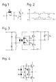
- Fig. 1 and Fig. 2 illustrate how with the help of a capacitor C 1 as a capacitance device and a diode D 1 as a semiconductor element, a transformer voltage signal U W1 generated by the transformer by means of an auxiliary winding W 1 in the manner of a voltage doubler for generating a drive voltage U V1 for the Power semiconductor component V 1 can be raised in such a way that, from a high (ie switch-on) level, the power semiconductor element is switched off periodically in rectifier mode in a synchronous and otherwise known manner.
- the signal peaks generated by the voltage doubling in the signal U V1 are harmless for an operation of the power semiconductor V 1 .
- the auxiliary winding is mounted in an otherwise known manner on the main transformer (not explained in more detail) and has a close coupling with its power windings.
- a pair of auxiliary windings W 1 , W 2 for a respective power semiconductor V 1 or V 2 generates an antiphase voltage signal in an otherwise known manner.
- the drive signal for the power semiconductors V 1 , V 2 is shown in the manner shown in FIG. 2, lower curve raised that a sufficient charge and thus voltage level is available for the desired control of the semiconductors.
- capacitor C 1 is dimensioned such that it exceeds a (parasitic) gate capacitance of the MOSFETs V 1 or V 2 by a multiple, so that the voltage drop across C 1 is only insignificant as a result of the control of the semiconductors decreases.
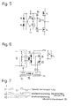
- FIGS. 1 to 3 A further development of the basic idea of FIGS. 1 to 3 is explained on the basis of FIGS. 4 and 5, the principle-related disadvantages of FIG. 3 being able to be improved by using (MOSFET) transistors instead of the diodes.
- the main disadvantages have already been set out above: the problem is that the capacitor voltage is an image of the input voltage, and if this varies, the capacitor voltage also changes. However, since the capacitance value C 1 must be chosen to be relatively large, the adaptation of the capacitor voltage can take a long time.
- the solution with (MOSFET) transistors acc. Fig. 4, Fig. 5 is advantageous because the transistors 30, 32 in Fig. 4, Fig. 5 (in particular MOSFETs) are in principle driven with low resistance in both "current directions" and can therefore quickly charge and discharge the capacitor ; thus the voltage on this capacitor always follows the input voltage, regardless of how it changes. (If this is not the case, there is a risk that the synchronous rectifier will no longer be switched off properly in the event of a negative input voltage jump.)
- each branch of the partial circuit shown in FIG. 4 has its own capacitor C 1 or C 2 has.
- a respective diode is replaced by a MOSFET 30, 32, such that the relevant channel of the MOSFET runs instead of the diode of FIG. 3, and the (gate) control of a relevant MOSFET is tapped by the signal on the opposite branch, ie MOSFET 32 is tapped by the signal at the node between W 1 and C 1 , while the control signal for MOSFET 30 is tapped at the node between W 2 and C 2 .
- MOSFET 30 ensures that when the power semiconductor V 1 is switched off, its gate electrode is pulled to zero potential with a low resistance (and this applies correspondingly to MOSFET 32 or V 2 ), with the effect that, in particular even in the case of fast ones Voltage changes at the drain electrode of the active rectifier elements V 1 , V 2 , these cannot turn on again due to parasitic (feedback) capacitances between the drain and gate.
- FIG. 4 is supplemented further by the fact that a semiconductor 34 or 36, preferably MOSFET, is also connected in the branch between the capacitor and the respective control electrode of the power semiconductor element for voltage limitation, which symbolically shown in FIG. is preset with a selected voltage U G and thus defines or limits a maximum control voltage for V 1 or V 2 .
- a semiconductor 34 or 36 preferably MOSFET
Landscapes
- Engineering & Computer Science (AREA)
- Power Engineering (AREA)
- Dc-Dc Converters (AREA)
- Rectifiers (AREA)
Applications Claiming Priority (2)
| Application Number | Priority Date | Filing Date | Title |
|---|---|---|---|
| DE10109768A DE10109768A1 (de) | 2001-03-01 | 2001-03-01 | Spannungskonverter |
| DE10109768 | 2001-03-01 |
Publications (2)
| Publication Number | Publication Date |
|---|---|
| EP1237268A2 true EP1237268A2 (fr) | 2002-09-04 |
| EP1237268A3 EP1237268A3 (fr) | 2004-12-29 |
Family
ID=7675873
Family Applications (1)
| Application Number | Title | Priority Date | Filing Date |
|---|---|---|---|
| EP01130956A Withdrawn EP1237268A3 (fr) | 2001-03-01 | 2001-12-28 | Convertisseur de tension |
Country Status (3)
| Country | Link |
|---|---|
| US (1) | US6657872B2 (fr) |
| EP (1) | EP1237268A3 (fr) |
| DE (1) | DE10109768A1 (fr) |
Families Citing this family (7)
| Publication number | Priority date | Publication date | Assignee | Title |
|---|---|---|---|---|
| GB0127586D0 (en) * | 2001-11-17 | 2002-01-09 | Advanced Power Conversion Ltd | DC-DC Converters |
| US7203041B2 (en) * | 2004-04-30 | 2007-04-10 | Power-One, Inc | Primary side turn-off of self-driven synchronous rectifiers |
| TWI384735B (zh) * | 2009-09-23 | 2013-02-01 | Chung Hsin Elec & Mach Mfg | 倍壓電路結構 |
| DE102012219365A1 (de) * | 2012-10-23 | 2014-04-24 | Schmidhauser Ag | Gleichspannungswandler |
| EP2963587B1 (fr) * | 2014-07-04 | 2017-03-15 | Nxp B.V. | Convertisseur de tension |
| US10439431B2 (en) | 2016-02-23 | 2019-10-08 | Vertiv Corporation | Method to reduce inrush currents in a transformer-less rectifier uninterruptible power supply system |
| US12283893B2 (en) * | 2022-12-20 | 2025-04-22 | Monolithic Power Systems, Inc. | Converter circuit with half-bridge current-doubler rectifier and integrated magnetics |
Family Cites Families (13)
| Publication number | Priority date | Publication date | Assignee | Title |
|---|---|---|---|---|
| US3866107A (en) * | 1974-01-28 | 1975-02-11 | Bendix Corp | Starting circuit for inverter |
| SU957368A1 (ru) * | 1980-12-23 | 1982-09-07 | Предприятие П/Я Г-4084 | Устройство дл управлени двухтактным транзисторным ключом |
| DE3727170A1 (de) * | 1987-08-14 | 1989-02-23 | Philips Patentverwaltung | Gleichspannungswandler mit einem uebertrager |
| ATE88304T1 (de) * | 1987-10-29 | 1993-04-15 | Rifala Pty Ltd | Umwandler mit hohem wirkungsgrad. |
| JPH09149636A (ja) * | 1995-11-20 | 1997-06-06 | Hitachi Ltd | スイッチング電源装置 |
| JP2000511040A (ja) * | 1997-03-12 | 2000-08-22 | コーニンクレッカ フィリップス エレクトロニクス エヌ ヴィ | 変換器、電源及びバッテリー充電器 |
| US6011703A (en) * | 1997-07-30 | 2000-01-04 | Lucent Technologies Inc. | Self-synchronized gate drive for power converter employing self-driven synchronous rectifier and method of operation thereof |
| JP3673075B2 (ja) * | 1998-03-09 | 2005-07-20 | 新電元工業株式会社 | スイッチング電源装置 |
| JP4381493B2 (ja) * | 1998-03-17 | 2009-12-09 | ソニー株式会社 | 電流共振型スイッチング電源 |
| US6084792A (en) * | 1998-08-21 | 2000-07-04 | Vpt, Inc. | Power converter with circuits for providing gate driving |
| US6091616A (en) * | 1998-10-21 | 2000-07-18 | Lucent Technologies Inc. | Drive compensation circuit for synchronous rectifier and method of operating the same |
| US6304461B1 (en) * | 2000-06-15 | 2001-10-16 | Supertex, Inc. | DC power converter having bipolar output and bi-directional reactive current transfer |
| CN1144346C (zh) * | 2000-08-17 | 2004-03-31 | 伊博电源(杭州)有限公司 | 同步整流管的自驱动电路 |
-
2001
- 2001-03-01 DE DE10109768A patent/DE10109768A1/de not_active Withdrawn
- 2001-12-28 EP EP01130956A patent/EP1237268A3/fr not_active Withdrawn
-
2002
- 2002-02-26 US US10/082,625 patent/US6657872B2/en not_active Expired - Fee Related
Also Published As
| Publication number | Publication date |
|---|---|
| EP1237268A3 (fr) | 2004-12-29 |
| US6657872B2 (en) | 2003-12-02 |
| DE10109768A1 (de) | 2002-09-05 |
| US20020122321A1 (en) | 2002-09-05 |
Similar Documents
| Publication | Publication Date | Title |
|---|---|---|
| DE102008032876B4 (de) | Verfahren, Schaltungsanordnung und Brückenschaltung | |
| DE2834512C2 (de) | Umformer mit ausschaltbaren Thyristoren | |
| DE1763820A1 (de) | Gleichspannungs-Gleichspannungs-Wandler | |
| EP2237404A1 (fr) | Onduleur avec deux ponts asymmetrics et une branche à roue libre découplante l'entrée du courant continu de la sortie du courant alternatif | |
| EP2852044B1 (fr) | Convertisseur bidirectionnel à direction préférentielle et onduleur capable de produire de la puissance reactive | |
| DE102007015302A1 (de) | Konverter, insbesondere für ein Ionentriebwerk | |
| AT515242B1 (de) | Verfahren zum Steuern eines Vollbrücken DC/DC-Wandlers | |
| EP2709257A2 (fr) | Circuit de convertisseur de courant et procédé de commande du circuit de convertisseur de courant | |
| DE102006012164B4 (de) | Schaltungsanordnung zur Erzeugung einer Wechselspannung oder eines Wechselstroms | |
| DE4421249C2 (de) | Schaltstromversorgungsgerät mit Snubber-Schaltung | |
| DE102010060508B4 (de) | Spannungswandler mit einer Speicherdrossel mit einer Wicklung und einer Speicherdrossel mit zwei Wicklungen | |
| EP0099596B1 (fr) | Circuit d'alimentation en courant électrique | |
| EP1237268A2 (fr) | Convertisseur de tension | |
| EP2992598A1 (fr) | Convertisseur élévateur ou abaisseur à condensateur de décharge | |
| DE19711017A1 (de) | Stromversorgungseinrichtung | |
| DE4001325B4 (de) | Gleichspannungssperrwandler | |
| WO2020152076A1 (fr) | Convertisseur continu-continu comprenant un circuit de pont pour la mise hors tension ainsi que procédé correspondant | |
| DE10257908A1 (de) | Getaktete Leistungsversorgung | |
| WO2022167192A1 (fr) | Convertisseur indirect monté en série sur le côté primaire et doté d'un circuit de verrouillage | |
| DE3049020C2 (de) | Regelbarer Gleichspannungswandler für Leistungsschaltnetzteile | |
| EP3120447A1 (fr) | Circuit électrique comprenant un demi-pont | |
| DE3833700C2 (fr) | ||
| DE102006016284A1 (de) | Schaltungsanordnung zur Umwandlung einer Gleichspannung in eine Wechselspannung oder einen Wechselstrom | |
| DE4019158C2 (de) | Schalteinrichtung für eine Spannungsquelle | |
| WO2013092286A2 (fr) | Cellule de commutation comportant une diode à décharge statique |
Legal Events
| Date | Code | Title | Description |
|---|---|---|---|
| PUAI | Public reference made under article 153(3) epc to a published international application that has entered the european phase |
Free format text: ORIGINAL CODE: 0009012 |
|
| AK | Designated contracting states |
Kind code of ref document: A2 Designated state(s): AT BE CH CY DE DK ES FI FR GB GR IE IT LI LU MC NL PT SE TR |
|
| AX | Request for extension of the european patent |
Free format text: AL;LT;LV;MK;RO;SI |
|
| PUAL | Search report despatched |
Free format text: ORIGINAL CODE: 0009013 |
|
| AK | Designated contracting states |
Kind code of ref document: A3 Designated state(s): AT BE CH CY DE DK ES FI FR GB GR IE IT LI LU MC NL PT SE TR |
|
| AX | Request for extension of the european patent |
Extension state: AL LT LV MK RO SI |
|
| 17P | Request for examination filed |
Effective date: 20050510 |
|
| AKX | Designation fees paid |
Designated state(s): DE GB |
|
| STAA | Information on the status of an ep patent application or granted ep patent |
Free format text: STATUS: THE APPLICATION IS DEEMED TO BE WITHDRAWN |
|
| 18D | Application deemed to be withdrawn |
Effective date: 20070703 |