EP1237016A2 - Réflecteur et dispositif LCD de type réflectif l'utilisant - Google Patents
Réflecteur et dispositif LCD de type réflectif l'utilisant Download PDFInfo
- Publication number
- EP1237016A2 EP1237016A2 EP02004688A EP02004688A EP1237016A2 EP 1237016 A2 EP1237016 A2 EP 1237016A2 EP 02004688 A EP02004688 A EP 02004688A EP 02004688 A EP02004688 A EP 02004688A EP 1237016 A2 EP1237016 A2 EP 1237016A2
- Authority
- EP
- European Patent Office
- Prior art keywords
- reflector
- protrusions
- layer
- inclination angle
- protrusion pattern
- Prior art date
- Legal status (The legal status is an assumption and is not a legal conclusion. Google has not performed a legal analysis and makes no representation as to the accuracy of the status listed.)
- Granted
Links
Images


Classifications
-
- G—PHYSICS
- G02—OPTICS
- G02B—OPTICAL ELEMENTS, SYSTEMS OR APPARATUS
- G02B5/00—Optical elements other than lenses
- G02B5/02—Diffusing elements; Afocal elements
- G02B5/0205—Diffusing elements; Afocal elements characterised by the diffusing properties
- G02B5/021—Diffusing elements; Afocal elements characterised by the diffusing properties the diffusion taking place at the element's surface, e.g. by means of surface roughening or microprismatic structures
-
- G—PHYSICS
- G02—OPTICS
- G02F—OPTICAL DEVICES OR ARRANGEMENTS FOR THE CONTROL OF LIGHT BY MODIFICATION OF THE OPTICAL PROPERTIES OF THE MEDIA OF THE ELEMENTS INVOLVED THEREIN; NON-LINEAR OPTICS; FREQUENCY-CHANGING OF LIGHT; OPTICAL LOGIC ELEMENTS; OPTICAL ANALOGUE/DIGITAL CONVERTERS
- G02F1/00—Devices or arrangements for the control of the intensity, colour, phase, polarisation or direction of light arriving from an independent light source, e.g. switching, gating or modulating; Non-linear optics
- G02F1/01—Devices or arrangements for the control of the intensity, colour, phase, polarisation or direction of light arriving from an independent light source, e.g. switching, gating or modulating; Non-linear optics for the control of the intensity, phase, polarisation or colour
- G02F1/13—Devices or arrangements for the control of the intensity, colour, phase, polarisation or direction of light arriving from an independent light source, e.g. switching, gating or modulating; Non-linear optics for the control of the intensity, phase, polarisation or colour based on liquid crystals, e.g. single liquid crystal display cells
- G02F1/133—Constructional arrangements; Operation of liquid crystal cells; Circuit arrangements
- G02F1/1333—Constructional arrangements; Manufacturing methods
- G02F1/1335—Structural association of cells with optical devices, e.g. polarisers or reflectors
-
- G—PHYSICS
- G02—OPTICS
- G02B—OPTICAL ELEMENTS, SYSTEMS OR APPARATUS
- G02B5/00—Optical elements other than lenses
- G02B5/02—Diffusing elements; Afocal elements
- G02B5/0205—Diffusing elements; Afocal elements characterised by the diffusing properties
- G02B5/021—Diffusing elements; Afocal elements characterised by the diffusing properties the diffusion taking place at the element's surface, e.g. by means of surface roughening or microprismatic structures
- G02B5/0221—Diffusing elements; Afocal elements characterised by the diffusing properties the diffusion taking place at the element's surface, e.g. by means of surface roughening or microprismatic structures the surface having an irregular structure
-
- G—PHYSICS
- G02—OPTICS
- G02B—OPTICAL ELEMENTS, SYSTEMS OR APPARATUS
- G02B5/00—Optical elements other than lenses
- G02B5/02—Diffusing elements; Afocal elements
- G02B5/0205—Diffusing elements; Afocal elements characterised by the diffusing properties
- G02B5/021—Diffusing elements; Afocal elements characterised by the diffusing properties the diffusion taking place at the element's surface, e.g. by means of surface roughening or microprismatic structures
- G02B5/0226—Diffusing elements; Afocal elements characterised by the diffusing properties the diffusion taking place at the element's surface, e.g. by means of surface roughening or microprismatic structures having particles on the surface
-
- G—PHYSICS
- G02—OPTICS
- G02B—OPTICAL ELEMENTS, SYSTEMS OR APPARATUS
- G02B5/00—Optical elements other than lenses
- G02B5/02—Diffusing elements; Afocal elements
- G02B5/0273—Diffusing elements; Afocal elements characterized by the use
- G02B5/0284—Diffusing elements; Afocal elements characterized by the use used in reflection
-
- G—PHYSICS
- G02—OPTICS
- G02B—OPTICAL ELEMENTS, SYSTEMS OR APPARATUS
- G02B5/00—Optical elements other than lenses
- G02B5/08—Mirrors
- G02B5/10—Mirrors with curved faces
-
- G—PHYSICS
- G02—OPTICS
- G02F—OPTICAL DEVICES OR ARRANGEMENTS FOR THE CONTROL OF LIGHT BY MODIFICATION OF THE OPTICAL PROPERTIES OF THE MEDIA OF THE ELEMENTS INVOLVED THEREIN; NON-LINEAR OPTICS; FREQUENCY-CHANGING OF LIGHT; OPTICAL LOGIC ELEMENTS; OPTICAL ANALOGUE/DIGITAL CONVERTERS
- G02F1/00—Devices or arrangements for the control of the intensity, colour, phase, polarisation or direction of light arriving from an independent light source, e.g. switching, gating or modulating; Non-linear optics
- G02F1/01—Devices or arrangements for the control of the intensity, colour, phase, polarisation or direction of light arriving from an independent light source, e.g. switching, gating or modulating; Non-linear optics for the control of the intensity, phase, polarisation or colour
- G02F1/13—Devices or arrangements for the control of the intensity, colour, phase, polarisation or direction of light arriving from an independent light source, e.g. switching, gating or modulating; Non-linear optics for the control of the intensity, phase, polarisation or colour based on liquid crystals, e.g. single liquid crystal display cells
- G02F1/133—Constructional arrangements; Operation of liquid crystal cells; Circuit arrangements
- G02F1/1333—Constructional arrangements; Manufacturing methods
- G02F1/1335—Structural association of cells with optical devices, e.g. polarisers or reflectors
- G02F1/133553—Reflecting elements
Definitions
- the present invention relates to a reflection-type Liquid-Crystal Display (LCD) device. More particularly, the invention relates to a reflector for a reflection-type LCD device that forms its light source by reflecting external incident light, and a LCD device using the reflector.
- LCD Liquid-Crystal Display
- reflection-type LCD devices are known well. Reflection-type LCD devices have an advantage that the power consumption is low and the body is thin and light, compared with transmission-type LCD devices. This is because external light can be used for their light source by reflecting it with a built-in reflector, which eliminates the backlight. Thus, reflection-type LCD devices are mainly used for portable electronic terminals such as portable telephones.
- the reflection-type LCD device comprises various modes or types, such as the twisted-nematic (TN) mode, the single polarizer type, the super twisted-nematic (STN) mode, the guest-host mode, the polymer-distributed liquid crystal (PDLC) type, and the cholesteric phase type.
- the basic configuration of the reflection-type LCD device comprises a liquid crystal layer, switching elements for driving the liquid crystal in the layer, and a reflector plate provided inside or outside the LCD cell.
- the active-matrix addressing method using Thin-Film Transistors (TFTs) or Metal/Insulator/Metal (MIM) diodes as the switching elements is employed along with the reflector. This is because it generates high resolution and high quality of image.
- TFTs Thin-Film Transistors
- MIM Metal/Insulator/Metal
- reflection-type LCD devices An example of the reflection-type LCD devices is as follows:
- An organic dielectric film is formed on a plate and then, the film is patterned by photolithography and etching processes, forming isolated protrusions on the surface of the plate.
- the protrusions are formed by the remaining organic film.
- An interlayer dielectric film is formed on the plate to cover the protrusions, making protrusions on the surface of the interlayer dielectric film, in other words, making a bumpy surface of the interlayer dielectric film.
- the Japanese Patent No. 2825713 issued on September 11, 1998 discloses another example of the reflection-type LCD devices.
- an organic dielectric film is formed over a plate and then, the film is patterned by photolithography and etching processes, forming protrusions on the surface of the film. Thereafter, a patterned metal film serving as a reflector electrode is formed on the dielectric film to cover the protrusions.
- a substrate with the reflector electrode whose surface is smoothly roughened is formed.
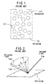
- Fig. 1 is a plan view showing a prior-art plate-shaped reflector 101, in which protrusions 102 are formed on the surface of the reflector 101. As shown in Fig. 1, all the protrusions 102 are circular in plan shape and arranged to be isolated from each other.
- the prior-art reflector 101 has a purpose of reflecting incident light while diffusing the same at a certain extent and therefore, the reflected light has large dispersion.
- the incident light is reflected in such a way that the reflected light is diffused within a conical region approximately uniformly, as shown in Fig. 2.
- Fig. 2 shows the relationship between the incident light and the reflected light by the prior-art reflector plate 101.
- the incident light L IN e.g., a fluorescent lamp or the sunlight
- the light L IN irradiated is reflected by the plate 101, forming reflected light beams L REF .
- the reflected beams L REF are approximately uniformly diffused by the reflector 101. Accordingly, the prior-art reflector 101 with the circular protrusions 102 has the following disadvantages.
- the prior-art reflector 101 when the prior-art reflector 101 is located in a situation (e.g., in a room) where direct light is dominant and indirect light is weak, part of the incident light L IN that propagates in a specific direction is not reflected efficiently toward the viewer.
- the "direct light” is strong light emitted from a light source, such as a fluorescent lamp, and directly irradiated to the reflector 101 without reflection.
- the "indirect light” is light emitted from a light source, such as a fluorescent lamp, and indirectly irradiated to the reflector 101 after reflection at some positions (e.g., a wall). This means that the incident light L IN is not utilized effectively.
- the intensity of the reflected right L REF toward the viewer decreases, resulting in the viewer's feeling that images on the displaying screen is dark or is not sufficiently light.
- the protrusions 102 of the reflector 101 have a specific geometric shape or arrangement pattern, there is a possibility that the color tone of images on the screen changes outstandingly according to the angle with respect to the LCD panel, the incident light L IN , and the position of the viewer. This is due to the optical interference caused by the difference between the optical path lengths of the beams of the reflected light L REF (i.e., which positions of the roughening pattern for the reflector 101 the incident light beam is reflected at). As a result, there is a possibility that the displaying performance of the LCD device of this type degrades.
- an object of the present invention is to provide a reflector for a reflection-type LCD device that reflects efficiently incident light to the viewer's side, and a reflection-type LCD device using the same.
- Another object of the present invention is to provide a reflector for a reflection-type LCD device that suppresses optical interference effectively, and a reflection-type LCD device using the same.
- Still another object of the present invention is to provide a reflector for a reflection-type LCD device that suppresses the change of color tone, and a reflection-type LCD device using the same.
- a further object of the present invention is to provide a reflector for a reflection-type LCD device that is easily designed, and a reflection-type LCD device using the same.
- a reflector for a reflection-type LCD device is provided.
- This reflector comprises a roughened surface having a protrusion pattern.
- the protrusion pattern gives inclination angle to the surface according to a specific distribution where a first component with an inclination angle value of 0° is 15% or less in area and a second component with an inclination angle value from 2° to 10° is 50% or greater in area.
- the roughened surface has the protrusion pattern that gives inclination angle to the surface according to a specific distribution.
- the distribution is determined in such a way that the first component with an inclination angle value of 0° is 15% or less in area and the second component with an inclination angle value from 2° to 10° is 50% or greater in area.
- the proportion of the reflected light traveling in a specific direction is increased. This means that the amount of the component of the reflected light that travels toward a viewer is increased. Accordingly, the incident light is efficiently reflected by the roughened surface of the reflector of the first aspect to the viewer's side.
- the specific distribution of the inclination angle values of the roughened surface has an average value within a range from 2° to 6°.
- the reflector can be fitted to a typical arrangement of light source in a circumstance or situation where the reflector is used, thereby optimizing the reflection efficiency.
- the reflector further comprises protrusions arranged in such a way that depressed areas are formed among adjoining ones of the protrusions, a first bumpy layer formed to cover the protrusions, and a base layer of the reflector formed on the first layer.
- Each of the depressed areas has a closed geometric shape.
- the first layer has a bumpiness generated by the protrusions.
- the base layer has a bumpiness corresponding to the bumpiness of the first layer, thereby forming the protrusion pattern of the surface of the reflector.
- the protrusions are arranged in such a way that the depressed areas, each of which has a closed geometric shape, are formed among adjoining ones of the protrusions. Moreover, the bumpiness of the first layer is generated by the protrusions. The bumpiness of the base layer corresponds to the bumpiness of the first layer, thereby forming the protrusion pattern of the surface of the reflector. As a result, the protrusion pattern of the surface of the reflector can be formed in such a way that protruding areas of the surface are distributed uniformly over the entire reflector.
- each of the depressed areas is like one selected from the group consisting of triangle, rectangular, and ellipse. In this case, there is an additional advantage that values of the protrusions and the depressed areas can be determined easily.
- each of the protrusions has a width W and a height D, where the width W and the height D have a relationship of 0.5 ⁇ ( D/W ) ⁇ 1.0.
- the shape of the protrusions is properly determined by the ratio ( D/W ), which determines the curvature of the surfaces of the protrusions. Therefore, the distribution of the incident angle values can be easily designed in such a way that the amount of the component of the reflected light that travels toward a viewer is increased.
- the ratio ( D/W ) is greater than 1.0, the total area of the protrusions with the inclination angle value of 10° or greater is likely to be excessive. If the ratio ( D/W ) is less than 0.5, the total area of the protrusions with the inclination angle value of 2° or less is likely to be excessive. As a result, the second component with the inclination angle value from 2° to 10° will be less than 50% in area. This leads to the viewer's feeling that the screen of the LCD device is not sufficiently light.
- the first bumpy layer has a minimum height d and the protrusions have an inter-center distance L, where the minimum height d and the inter-center distance L have a relationship of (1/20) ⁇ ( d/L ) ⁇ (1/5).
- the shape of the protrusions is properly determined by the ratio ( d/L ), which determines the curvature of the surfaces of the protrusions. Therefore, the distribution of the incident angle values can be easily designed in such a way that the amount of the component of the reflected light that travels toward a viewer is increased.
- the ratio ( d/L ) is greater than (1/5), the total area of the protrusions with the inclination angle value of 10° or greater is likely to be excessive. If the ratio ( d/L ) is less than (1/20), the total area of the protrusions with the inclination angle value of 2° or less is likely to be excessive. As a result, the second component with the inclination angle value from 2° to 10° will be less than 50% in area. This leads to the viewer's feeling that the screen of the LCD device is not sufficiently light.
- each of the protrusions has a height D and the first bumpy layer has a minimum height d, where the height D and the minimum height d have a relationship of ( D/d ) ⁇ 3.
- the shape of the protrusions is properly determined by the ratio ( D/d ), which determines the curvature of the surfaces of the protrusions. Therefore, the distribution of the incident angle values can be easily designed in such a way that the amount of the component of the reflected light that travels toward a viewer is increased.
- the ratio ( D/d ) is greater than 3, the total area of the protrusions with the inclination angle value of 10° or greater is likely to be excessive. As a result, the second component with the inclination angle value from 2° to 10° will be less than 50% in area. This leads to the viewer's feeling that the screen of the LCD device is not sufficiently light.
- the protrusions included in a single pixel have a single maximum value of height.
- the protrusions included in a single pixel have a single maximum value of height
- the first component with the inclination angle value of 0° of the protrusion pattern which is typically located right above the top of the protrusion or the bottom of the depressed area, will be decreased in area. This leads to the viewer's feeling that the screen of the LCD device is not sufficiently light.
- the distribution of the incident angle values can be easily designed in such a way that the amount of the component of the reflected light that travels toward a viewer is increased.
- another reflector for a reflection-type LCD device is provided.
- This reflector comprises a roughened surface having a protrusion pattern.
- the protrusion pattern gives a variation range of chromaticity coordinates (x, y) on a chromaticity diagram dependent on an angle of view.
- the variation range is limited in a circle on the chromaticity diagram.
- the circle has a radius of approximately 0.05 and a center at a point corresponding to white color.
- the roughened surface has the protrusion pattern that gives a variation range of chromaticity coordinates (x, y) on the chromaticity diagram dependent on the angle of view.
- the variation range is limited in the circle on the chromaticity diagram.
- the circle has a radius of approximately 0.05 and a center at a point corresponding to white color.
- optical interference can be suppressed effectively. This means that the variation of color tone due to optical interference can be suppressed.
- the optical characteristics of the reflector can be easily known with a measuring apparatus, not with labor, by way of measuring the variation of chromaticity coordinates (x, y) on the chromaticity diagram.
- the reflector further comprises protrusions arranged in such a way that depressed areas are formed among adjoining ones of the protrusions, a first bumpy layer formed to cover the protrusions, and a base layer of the reflector formed on the first layer.
- Each of the depressed areas has a closed geometric shape.
- the first layer has a bumpiness generated by the protrusions.
- the base layer has a bumpiness corresponding to the bumpiness of the first layer, thereby forming the protrusion pattern of the surface of the reflector.
- each of the depressed areas is like one selected from the group consisting of triangle, rectangular, and ellipse. In this case, there is an additional advantage that values of the protrusions and the depressed areas can be determined easily.
- the first bumpy layer has a minimum height d and the protrusions have an inter-center distance L , where the minimum height d and the inter-center distance L have a relationship of (1/15) ⁇ ( d/L ).
- the shape of the protrusions is properly determined by the ratio ( d/L ), which determines the curvature of the surfaces of the protrusions. Therefore, the distribution of the incident angle values can be easily designed in such a way that the amount of the component of the reflected light that travels toward a viewer is increased.
- the ratio ( d/L ) is greater than (1/15)
- the inclination angle value is increased and the curvature of the protrusions is decreased.
- the positional dispersion of the bright spots or bright regions will be small, which means that the dispersion of the wavelength is unable to be cancelled as desired.
- the change of color tone will be conspicuous.
- the protrusion pattern gives a specific distribution of inclination angle values to the surface.
- incident light is irradiated to the surface of the reflector, bright regions with specific extent are generated, each of which has an inclination angle value within a range from 2° to 6°.
- the bright regions with specific extent are generated.
- Each of the regions has an inclination angle value within a range from 2° to 6°.
- the regions can be arranged in such a way as to cover or compensate the wavelength variation of the reflected light corresponding to the change of color tone thereof. This means that the distribution of the inclination angle values can be easily designed or determined to suppress the change of color tone dependent on the angle of view.
- the bright regions include a closest bright region.
- the regions can be surely arranged in such a way as to cover or compensate the wavelength variation of the reflected light corresponding to the change of color tone thereof.
- the distribution of the inclination angle values can be easily designed or determined to suppress the change of color tone dependent on the angle of view.
- each of the depressed areas is like one selected from the group consisting of triangle, rectangular, and ellipse.
- L min , L max , and L mean can be determined easily.
- a reflection-type LCD device comprises one of the reflectors according to the first and second aspects of the invention described above.
- reflection-type LCD device since one of the reflectors according to the first and second aspects of the invention is used, desired brightness is obtainable in typical situations of use of the device and/or the change of color tone dependent on the angel of view is suppressed.
- Fig. 1 is a schematic plan view showing a prior-art reflector having protrusions on its surface.
- Fig. 2 is a schematic view showing the relationship between the incident light and the reflected light by the prior-art reflector of Fig. 1.
- Fig. 3 is a schematic, partial cross-sectional view showing the configuration of a reflection-type LCD device according to an embodiment of the invention, in which the partial configuration corresponding to one of the pixels is mainly shown.
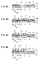
- Figs. 4A to 4D are schematic, partial cross-sectional views showing the process steps of a method of fabricating the reflection-type LCD device according to the embodiment of Fig. 3, respectively.
- Fig. 5A is a schematic side view showing the relationship between the incident light and the reflected light by the reflector according to the embodiment of the invention.
- Fig. 5B is an enlarged, schematic side view showing the relationship between the incident light and the reflected light by the reflector according to the embodiment of the invention.
- Fig. 6A is a schematic side view showing the relationship between the incident light, the viewer, and the reflector according to the embodiment of the invention.
- Fig. 6B is a schematic perspective view showing the relationship between the incident light, the viewer, and the reflector according to the embodiment of the invention.
- Fig. 7 is a schematic plan view showing the protrusion pattern of the second dielectric layer formed to cover the underlying protrusions in the LCD device of Fig. 3, which is substantially the same as the protrusion pattern of the reflector according to the embodiment of the invention.
- Fig. 8 is an enlarged, schematic cross-sectional view showing the detailed structure of the protrusion pattern of the second dielectric layer formed to cover the underlying protrusions in the LCD device of Fig. 3, which is substantially the same as the protrusion pattern of the reflector according to the embodiment of the invention.
- Fig. 9 is a graph showing the distribution of the incident angle values of the protrusions of the samples of the reflector.
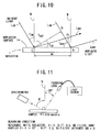
- Fig. 10 is a schematic side view explaining the cause of optical interference in the reflector according to the embodiment of the invention.
- Fig. 11 is a schematic side view showing the method of measuring the optical characteristics of the reflector according to the embodiment of the invention.
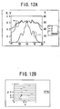
- Fig. 12A is a graph showing the emission angle dependence of the brightness (Y) of the sample 1 of the reflector.
- Fig. 12B is a graph showing the emission angle dependence of the color coordinates (x, y) of the sample 1 of the reflector.
- Fig. 12C is a graph showing the emission angle dependence of the brightness (Y) of the sample 2 of the reflector.
- Fig. 12D is a graph showing the emission angle dependence of the color coordinates (x, y) of the sample 2 of the reflector.
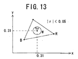
- Fig. 13 is a graph showing the permissible range of the color coordinates (x, y) of the reflector according to the embodiment of the invention.
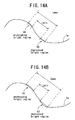
- Fig. 14A is a schematic view showing the bright regions of the bumpy surface of the reflector according to the embodiment of the invention, where the protruding and depressed bright regions are comparatively narrow.
- Fig. 14B is a schematic view showing the bright regions of the bumpy surface of the reflector according to the embodiment of the invention, where the protruding and depressed bright regions are comparatively wide.
- Fig. 15A is a graph showing the distribution of the height of the bumpy surface of the reflector according to the embodiment of the invention, as a function the position or distance.
- Fig. 15B is a graph showing the distribution of the inclination angle of the bumpy surface of the reflector according to the embodiment of the invention, as a function the position or distance.
- Fig. 16 is a schematic plan view showing a variation of the protrusion pattern of the second dielectric layer formed to cover the underlying protrusions in the LCD device of Fig. 3.
- Fig. 17 is a schematic plan view showing another variation of the protrusion pattern of the second dielectric layer formed to cover the underlying protrusions in the LCD device of Fig. 3.
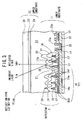
- a reflection-type LCD device 10 has the configuration as shown in Fig. 3, in which the structure corresponding to one of the pixels is illustrated. As seen from Fig. 3, this device 10 comprises a lower substrate 11, an opposite or upper substrate 12 located to be opposite to the lower substrate 11, and a liquid-crystal (LC) layer 13 sandwiched by the substrates 11 and 12.
- LC liquid-crystal
- the LCD device 10 includes thin-film transistors (TFTs) 16 as the switching elements for turning on and off the respective pixels.
- TFTs thin-film transistors
- only one TFT 16 is shown in Fig. 3.
- the device 10 has a plurality of TFTs 16 arranged in a matrix array.
- the lower substrate 11 comprises a dielectric plate 14, a dielectric protection layer 15, the TFTs 16, a first dielectric layer 17, approximately conical protrusions 18, a second dielectric layer 19, reflector electrodes 20, and contact holes 21. Since the TFTs 16 are formed on the substrate 11, the substrate 11 may be termed the "TFT substrate".
- the dielectric protection layer 15 is formed on the dielectric plate 14.
- the TFTs 16 are formed regularly on the plate 14. Each of the TFTs 16 has a gate electrode 16a, a drain electrode 16b, a patterned semiconductor layer 16c, and a source electrode 16d.
- the gate electrode 16a is formed on the plate 14.
- the drain electrode 16b is formed on the protection layer 15 that covers the gate electrode 16a.
- the semiconductor layer 16c is formed on the protection layer 15 to be entirely overlapped with the gate electrode 16a.
- the source electrode 16d is formed on the protection layer 15 to be apart from the drain electrode 16b.
- the semiconductor layer 16c is located between the drain and source electrodes 16b and 16d to be contacted with them.
- the first dielectric layer 17, which is formed to cover the TFTs 16, has penetrating contact holes 17a that expose the corresponding source electrodes 16d.
- the protrusions 18 are located on the layer 17 and the exposed source electrodes 16d in such a way as to be isolated from each other.
- the second dielectric layer 19 is formed on the first dielectric layer 17 and the exposed source electrodes 16d to cover the protrusions 18. Because of the existence of the underlying protrusions 18, the layer 19 has specific protrusions (i.e., a specific unevenness) on its surface; in other words, the surface of the layer 19 is bumpy. The layer 19 has the contact holes 21 that expose the corresponding source electrodes 16d while none of the protrusions 18 are exposed.
- the reflector electrodes 20 are formed on the second dielectric layer 19 to be overlapped with the TFTs 16 and the contact holes 21 of the layer 19.
- the electrodes 20 are contacted with and electrically connected to the corresponding source electrodes 16d by way of the corresponding contact holes 21.
- Each of the electrodes 20 serves as a reflector and a pixel electrode.
- gate terminals 22 and drain terminals 23 are formed in the terminal area of the lower substrate 11, which is located in the periphery of the substrate 11.
- the gate terminals 22, which are located on the plate 14, are contacted with and electrically connected to corresponding, overlying scan lines 22a.
- the drain terminals 23, which are located on the protection layer 15, are contacted with and electrically connected to corresponding, overlying data lines 23a.
- the opposing, upper substrate 12 comprises a transparent electrode 24, a color filter 25, and a transparent, dielectric plate 26.
- the filter 25 is formed on the plate 26.
- the electrode 24 is formed on the filter 25. Since the filter 25 is formed on the substrate 12, the substrate 12 may be termed the "color filter substrate".
- the lower and upper substrates 11 and 12 are fixed together at a specific distance.
- the LC layer 13 is located in the gap formed by the substrates 11 and 12.
- Incident light L IN which is irradiated from the outside of the LCD device 10 to the upper substrate 12, penetrates the substrate 12 to enter the LC layer 13. Then, the light L IN reaches the reflector electrode 20 of the lower substrate 11 by way of the layer 13 and then, reflected toward the substrate 12. Thus, the reflected light L REF is generated. The reflected light L REF thus generated travels through the LC layer 13 and the substrate 12 and then, goes out of the device 10.
- the protrusions 18, the second dielectric layer 19, and the reflector electrode 20 constitute a reflector of the embodiment.
- the reflector may have any other structure than this.
- the TFTs 16 as the switching elements are formed on the dielectric plate 14 of the lower substrate 11 by a known method.
- the gate electrodes 6a are formed on the plate 14 and then, the dielectric protection layer 15 is formed on the plate 14 to cover the gate electrodes 16a. Thereafter, the semiconductor layers 16c are formed on the layer 15 to be overlapped with the corresponding gate electrodes 16a. Furthermore, the drain and source electrodes 16b and 16c are formed on the layer 15 to contact with the corresponding semiconductor layers 16c, resulting in the TFTs 16. Finally, the first dielectric layer 17 is formed to cover the TFTs 16 thus formed and then, the contact holes 17a are formed to penetrate the same. The source electrodes 16d are exposed from the layer 17 by way of the holes 17a. The state at this stage is shown in Fig. 4A.
- the surface of the first dielectric layer 17 is planarized according to the necessity.
- the TFT 16 may be replaced with any other switching element, such as a diode.
- an organic resin layer (not shown) for the protrusions 18 is formed by a coating process on the first dielectric layer 17 and the exposed source electrodes 16d.
- the organic resin layer thus formed is then patterned by known optical exposure and development methods.
- frustum-shaped protrusions 18a are formed on the first dielectric layer 17 and the exposed source electrodes 16d.
- the state at this stage is shown in Fig. 4B.
- the frustum-shaped protrusions 18a which are made of the remaining organic resin layer, are subjected to a sintering process at a specific high temperature. Through this process, the top corners of the protrusions 18a are rounded. As a result, the protrusions 18 are made approximately conical. The state at this stage is shown in Fig. 4C.
- An organic resin layer (not shown) serving as an interlayer dielectric layer is formed by a coating process to cover the protrusions 18 and then, the contact holes 21 are formed in the organic resin layer thus formed by known optical exposure and development methods. Thereafter, the organic resin layer is subjected to a sintering process at a specific high temperature, thereby forming the second dielectric layer 19. The state at this stage is shown in Fig. 4D.
- an aluminum (Al) film (not shown) is formed on the second dielectric layer 19 with the contact holes 21 and then, is patterned to form the reflector electrodes 20, as shown in Fig. 1.
- the A1 film may be replaced with any other conductive film.
- Each of the electrodes 20 includes protrusions or unevenness according to the underlying protrusions 18.
- the protrusions 18 are formed by pattering the organic resin layer.
- the protrusions 18 may be formed by patterning two or more stacked organic resin layers.
- the plan shape of the protrusions 18 will change through the exposure and development processes for the organic resin layer for the protrusions 18 and the sintering process therefor.
- the difference of the plan shape of the protrusions 18 will not cause any substantial change of the resultant protrusions or unevenness of the reflector electrodes 20.
- the plan shape of the protrusions 18 is rectangular, the change of the distance between the adjacent protrusions 18 will not cause any substantial change of the resultant protrusions or unevenness of the electrodes 20, regardless of the long sides of each rectangle being equal or not.
- Fig. 5A shows the state that the incident light L IN emitted from the light source S is reflected by the roughened or bumpy surface 1a of the reflector 1 according to the embodiment of the invention, thereby forming reflected light L REF , and that the reflected light L REF thus formed is observed by the viewer P.
- the bumpy surface 1a of the reflector 1 is formed by the underlying protrusions 18 explained above.
- the incident light L IN has an incident angle T IN defined as the angle between the incident light L IN and the normal N of the reflector 1.
- the reflected light L REF has a reflection angle T REF defined as the angle between the reflected light L REF and the normal of the reflector 1. Since the incident light L IN is reflected by the bumpy surface 1a of the reflector 1, the incident angle T IN is usually unequal to the reflection angle T REF .
- Fig. 5B schematically shows the enlarged state that the incident light L IN is reflected by the surface 1a of the reflector 1 according to the embodiment of the invention.
- the incident light L IN is reflected at the point A on the surface 1a, it is reflected by the tangent plane TP of the surface 1a.
- the reflected light L REF is formed symmetrically with respect to the normal N' of the tangent plane TP at the point A.
- the angle between the reference plane RP of the reflector 1 and the tangent plane TP at the point A is defined as the "inclination angle ⁇ at the point A”. Then, the distribution of the reflection direction of the reflected light L REF is dependent on the inclination angle ⁇ . Therefore, it is important that the viewer P evaluates subjectively the brightness of the reflector 1 and that the inclination angle ⁇ is determined'in such a way that the viewer P recognizes the reflection state as sufficiently bright one.
- the incident angle TIN is within the range from 0° to -60° while the reflection angle T REF is within the range from -10° to 20°.
- the incident angle T IN ' in the horizontal direction is within the range from -20° to 20° while the reflection angle T REF ' in the horizontal direction is within the range from -20° to 20°.
- the reflector 1 can be designed to have a satisfactory directionality in such a way that the incident light L IN from the light source S is effectively turned to the reflected light L REF traveling toward the viewer P. As a result, the reflector 1 can be suitable to the situation of Figs. 6A and 6B.
- Fig. 7 shows an example of the protrusion pattern of the second dielectric layer 19 formed to cover the underlying protrusions 18 in the LCD device 10 of Fig. 3. Since the Al layer (i.e., the reflector electrode 20) formed on the layer 19 is very thin, the protrusion pattern of the reflector 1 according to the embodiment is substantially the same as that of the layer 19.
- the hatched area 51 denotes the protrusions of the surface of the second dielectric layer 19 while the non-hatched triangular areas 52 denote depressed areas thereof.
- the protrusions 51 which are approximately linear, are connected to each other.
- the depressed areas 52 are arranged at a specific level of disorder.
- the edges of the protrusions 51 constitute the sides of the triangular'depressed areas 52.
- approximately linear protrusions 51 which are unified together, constitute the triangular depressed areas 52.
- the invention is not limited this. It is sufficient for the invention that approximately linear protrusions 51 constitute closed geometric shapes (e.g., triangle, rectangle, square, circle, or ellipse) corresponding to depressed areas 52.
- Fig. 8 schematically shows the partial cross section of the second dielectric layer 19 and the protrusions 18 in the device 10 between the points P1 and P2 in Fig. 7.
- the protrusions 51 of the layer 19 are formed by the corresponding protrusions 18 of the device 10.
- the depressed areas 52 of the layer 19 are formed by the corresponding depressed areas between the adjoining protrusions 18.
- the distance between the adjoining protrusions 18 is defined as L, and the width and height of the protrusions 18 are defined as W and D , respectively.
- the minimum height of the second dielectric layer 19 is defined as d .
- the height D and the minimum height d are measured with reference to the reference plane 53.
- the plane 53 is determined as a plane in which the height of the layer 19 is minimum.
- the height difference of the layer 19 between the maximum and minimum points is defined as ⁇ D.
- the reflector electrode 20 is formed on the second dielectric layer 19, it is omitted from Fig. 8. This is because the electrode 20, which is made of the Al film, is actually very thin.
- the inventors To subjectively evaluate the effect of the reflector 1, the inventors fabricated samples of the reflector 1 as shown in Figs. 7 and 8 while changing the values of L, W, D, d, and ⁇ D. Thereafter, they built the samples thus fabricated into the LCD device 10 of Fig. 3 and evaluated subjectively the brightness and interference thereof. The result of this subjective evaluation test is shown in Table 1 below.
- the shape of the protrusions 51 (18) is determined by the ratio of the height D of the protrusions 51 (18) to the width W thereof, i.e., ( D/W ), which determines the curvature of the protrusions 51 (18). Therefore, the distribution of the values of the inclination angle ⁇ (see Fig. 5B) can be designed as desired. If the ratio ( D/W ) is greater than 1.0, the value of the angle ⁇ is likely to be too large. If the ratio ( D/W ) is less than 0.5, the value of the angle ⁇ is likely to be too small.
- the relationship of (1/20) ⁇ (d/L) ⁇ (1/5) is preferably satisfied.
- the shape of the bumpy surface of the second dielectric layer 19 is determined by the ratio of the minimum height d of the protrusions 18 the inter-center distance L thereof, i.e., ( d/L ), which determines the curvature of the surface of the layer 19. Therefore, the distribution of the values of the inclination angle ⁇ can be designed as desired. If the ratio ( d/L ) is greater than 1/5, the value of the angle ⁇ is likely to be too large. If the ratio ( d/L ) is less than 1/20, the value of the angle ⁇ is likely to be too small.
- the shape of the bumpy surface of the second dielectric layer 19 is determined by the ratio of the minimum height d of the layer 19 to the height D thereof, i.e., ( D/d ), which determines the curvature of the surface of the layer 19. Therefore, the distribution of the values of the inclination angle ⁇ can be designed as desired. If the ratio ( D/d ) is greater than 3, the value of the angle ⁇ is likely to be too large.
- Fig. 9 shows the distribution of the inclination angle ⁇ of the good reflectors 1 (the reflector electrodes 20) and the bad ones from the result of the above-described subjective evaluation test.
- the curve A for the good ones 50% or greater of the measured values of the inclination angle ⁇ are within the range from 2° to 10°.
- the curve B for the bad ones 15% or greater of the measured values of the inclination angle ⁇ were 0°.
- the bottom of the second dielectric layer 19 having the minimum height d and/or the top of the layer 19 having the maximum height ( d + ⁇ D ) is/are wide, it/they tend(s) to be partially flat.
- the total area i.e., size
- the height distribution of the second dielectric layer 19 i.e. the bumpy surface 1a of the reflector 1 are not maximized at both the top and bottom of the layer 19.
- the "bright spots” means the positions on the surface 1a of the reflector 1 the viewer P recognizes bright due to reflection of the beams of the incident light L IN at the surface 1a.
- optical interference occurs between the triangular depressed area 52 and the adjoining protruding part 51.
- optical interference occurs between the adjoining triangular depressed areas 52 or between the adjoining protruding parts 51.
- the pitch m of the depressed area 52 and the adjoining protruding part 51 is approximately 3 ⁇ m
- the pitch of the adjoining protruding parts 51 is approximately 10 ⁇ m
- the height difference h between the depressed area 52 and the adjoining part 51 is approximately 0.5 ⁇ m. Therefore, here, it is supposed that the pitch m is much greater than the height difference h, i.e., m >> h, and thus, the height difference h is ignored for simplification in the following explanation for simplification.
- Fig. 10 schematically shows the optical paths of the beams of the incident light L IN and the beams of the reflected light L REF , where the inclination angle ⁇ at the points A and C is equal and the reflected beams L REF are in the same direction as the incident beams L IN .
- the wavelength of the incident beams L IN is defined as ⁇ .
- the phase difference ⁇ of the adjoining reflected beams L REF that cause optical interference satisfies the following equation, where n is a natural number.
- the intensity I of the resultant reflected light varies dependent on the wavelength ⁇ of the incident beams L IN .
- the viewer P recognizes the light of a wavelength strongly and the light of another wavelength weakly.
- the images the viewer P recognizes on the screen of the device 10 includes conspicuous change of color tone.
- the emission or reflection angle T REF of the reflected light L REF that induces constructive interference is given as shown in Table 5, where the pitch m is used as a parameter.
- the first peak was found at the emission or reflection angle T REF of approximately 36°. Therefore, the effective value of the pitch m that induces no optical interference was greater than approximately 3 ⁇ m (i.e., m > 3 ⁇ m). Since the pitch of the protruding parts 51 and that of the depressed areas 52 are approximately 10 ⁇ m, it was considered that optical interference is caused by the adjoining protruding part and the depressed area, and that the effect by the adjoining protruding parts 51 and the adjoining depressed areas 52 is ignorable.
- Fig. 11 shows a method of measuring the optical characteristics of the reflector 1 according to the embodiment of the invention, which was carried by the inventors.
- Figs. 12A and 12C show the emission (reflection) angle dependence of the Y value (i.e., brightness) and the chromaticity coordinates (x, y) of the samples 1 and 2, respectively.
- Figs. 12B and 12D show the chromaticity coordinates (x, y) of the samples 1 and 2 plotted on the x,y chromaticity diagram, respectively.
- the variation of (x, y) of the sample 1 is limited within the range where ⁇ x is less than approximately 0.05 and ⁇ y is less than approximately 0.05 (i.e., ⁇ x ⁇ approximately 0.05, ⁇ y ⁇ approximately 0.05).
- the variation of (x, y) of the sample 2 is limited within the range where ⁇ x is increased to approximately 0.1 and ⁇ y is increased to approximately 0.1 (i.e., ⁇ x ⁇ approximately 0.1, ⁇ y ⁇ approximately 0.1). Therefore, it is seen that the level of strength of optical interference of the sample 2 is higher than that of the sample 1.
- the x and y coordinates of white may be (0.29 - 0.33, 0.29 - 0.33), in other words, each of the x and y coordinates may be changed within the range of 0.29 to 0. 33, according to the color temperature.
- Figs. 14A and 14B show the protruding bright region 61 and the depressed bright region 62 of the same elemental shape (or, the protruding part 51 and the adjoining depressed area 52 in Fig. 7) of the reflector 1 of the embodiment, where these two bright regions 61 and 62 have approximately equal values of the inclination angle ⁇ .
- the protruding bright region 61 and the depressed bright region 62 have approximately the same inclination angles, optical interference will occur according to the model of Fig. 10.
- the regions 61 and 62 have specific scope wider than a spot and thus, the phase difference of the overall reflected light is formed by Superposition of the reflected light beams at all the protruding and depressed bright regions 61 and 62 of the reflector 1.
- the minimum and maximum distances between the protruding bright region 61 and the adjoining depressed bright region 62 are defined as L min and L max , respectively.
- the dispersion of the regions 61 and 62 is given as ( L max + L min )/ L mean . It is preferred that the dispersion of the bright regions 61 and 62, i.e., [( L max + L min ) / L mean ], is designed to cancel the dispersion of the wavelength.
- the curvature of the bumpy surface 1a of the reflector 1 can be determined well. This means that the inclination angles of the regions 61 and 62 can be designed as desired. If ( d/L ) is equal to or less than (1/15), the inclination angle is likely to be too large and the curvature be too small, resulting in the dispersion of the bright regions 61 and 62 being too small. Thus, it is preferred that the relationship of ( d/L ) > (1/15) is satisfied.
- Fig. 15A shows the height change of the surface 1a as a function of the distance along the line P1P2.
- Fig. 15B shows the inclination angle change of the surface 1a as a function of the distance along the line P1P2.
- the bold lines A1, A2, B1, and B2 on the curve denote the areas having the inclination angle from 2° to 6°.
- the bold lines A1 and A2 correspond to the bright regions 61 and 62 near the corner of the triangular depressed area 52 in Fig. 7, respectively.
- the bold lines B1 and B2 correspond to the bright regions 61 and 62 near the base of the triangular area 52 in Fig. 7, respectively.
- This value of wavelength dispersion of 0.2 can be effectively canceled by the value of the dispersion of the bright regions 61 and 62 of 1.0.
- wavelength dispersion of 0.2 is not effectively canceled by the value of the dispersion of the bright regions 61 and 62 of approximately 0.3.
- the roughening pattern comprises triangular depressed areas 52
- each area 52 may have any closed geometric shape other than triangle, e.g., rectangle or ellipse, as shown in Figs. 16 and 17.
- the inclination angle of the protruding bright regions 61 and the depressed bright regions 62 are controlled
- the roughened surface 1a of the reflector 1 has the protrusion pattern that gives inclination angle to the surface 1a according to the specific distribution.
- the distribution is determined in such a way that the first component with an inclination angle value ⁇ of 0° is 15% or less in area and the second component with an inclination angle value ⁇ from 2° to 10° is 50% or greater in area.
- the proportion of the reflected light L REF traveling in a specific direction is increased.
- the amount of the component of the reflected light L REF that travels toward the viewer is increased. Accordingly, the incident light L IN is efficiently reflected by the roughened surface 1a of the reflector 1 of the embodiment to the viewer's side.
- the distribution of the incident angle values can be easily designed in such a way that the amount of the component of the reflected light that travels toward a viewer is increased.
- the visibility is improved over the whole surface of the reflector.
- the specific distribution of the inclination angle values of the roughened surface 1a has an average value within a range from 2° to 6°, there is an additional advantage that the reflector can be fitted to a typical arrangement of light source in a circumstance or situation where the reflector is used, thereby optimizing the reflection efficiency.
- the roughened surface 1a of the reflector 1 has the protrusion pattern that gives a variation range of chromaticity coordinates (x, y) on the chromaticity diagram dependent on the angle of view, and the variation range is limited in the circle on the chromaticity diagram, where the circle has a radius of approximately 0.05 and a center at a point corresponding to white color, optical interference can be suppressed effectively. This means that the variation of color tone due to optical interference can be suppressed.
- the optical characteristics of the reflector 1 can be easily known with a measuring apparatus, not with labor, by way of measuring the variation of chromaticity coordinates (x, y) on the chromaticity diagram.
- Figs. 16 and 17 show variations of the protrusion pattern of the second dielectric layer 19 formed to cover the underlying protrusions 18 in the LCD device 10 of Fig. 3.
- the depressed areas 52 are triangular. Unlike this, the depressed areas 52 are rectangular in the variation of Fig. 16 while the depressed areas 52 are elliptic in the variation of Fig. 17. In these variations, the same advantage as those in the above-embodiment is obtainable.
- the present invention is not limited to the above-described embodiment. Any change or modification may be added to the embodiment within the spirit of the invention.
- the reflector 1 comprises the protrusions 18, the second dielectric layer 19, and the reflector electrode 20 in the LCD device of the above embodiment, it may have any other structure than this.
Landscapes
- Physics & Mathematics (AREA)
- General Physics & Mathematics (AREA)
- Optics & Photonics (AREA)
- Nonlinear Science (AREA)
- Mathematical Physics (AREA)
- Chemical & Material Sciences (AREA)
- Crystallography & Structural Chemistry (AREA)
- Liquid Crystal (AREA)
- Optical Elements Other Than Lenses (AREA)
Applications Claiming Priority (2)
| Application Number | Priority Date | Filing Date | Title |
|---|---|---|---|
| JP2001055229 | 2001-02-28 | ||
| JP2001055229A JP2002258272A (ja) | 2001-02-28 | 2001-02-28 | 反射板並びに反射型液晶表示装置 |
Publications (3)
| Publication Number | Publication Date |
|---|---|
| EP1237016A2 true EP1237016A2 (fr) | 2002-09-04 |
| EP1237016A3 EP1237016A3 (fr) | 2005-01-12 |
| EP1237016B1 EP1237016B1 (fr) | 2013-04-03 |
Family
ID=18915439
Family Applications (1)
| Application Number | Title | Priority Date | Filing Date |
|---|---|---|---|
| EP02004688A Expired - Lifetime EP1237016B1 (fr) | 2001-02-28 | 2002-02-28 | Réflecteur et dispositif LCD de type réflectif l'utilisant |
Country Status (6)
| Country | Link |
|---|---|
| US (2) | US7092051B2 (fr) |
| EP (1) | EP1237016B1 (fr) |
| JP (1) | JP2002258272A (fr) |
| KR (1) | KR100454722B1 (fr) |
| NO (1) | NO335108B1 (fr) |
| TW (1) | TWI279618B (fr) |
Cited By (1)
| Publication number | Priority date | Publication date | Assignee | Title |
|---|---|---|---|---|
| JPWO2021186822A1 (fr) * | 2020-03-18 | 2021-09-23 |
Families Citing this family (9)
| Publication number | Priority date | Publication date | Assignee | Title |
|---|---|---|---|---|
| US6816216B2 (en) * | 2001-04-12 | 2004-11-09 | Omron Corporation | Optical component and reflective plate, and device using the same optical component |
| KR100483979B1 (ko) | 2001-06-22 | 2005-04-18 | 엔이씨 엘씨디 테크놀로지스, 엘티디. | 반사판, 그 제조방법, 액정표시장치 및 그 제조방법 |
| JP3990141B2 (ja) | 2001-11-08 | 2007-10-10 | Nec液晶テクノロジー株式会社 | 液晶表示装置 |
| KR100737895B1 (ko) * | 2002-09-18 | 2007-07-10 | 삼성전자주식회사 | 반사형 및 반사-투과형 액정표시장치 및 이의 제조방법 |
| JP4480599B2 (ja) | 2005-02-14 | 2010-06-16 | Nec液晶テクノロジー株式会社 | 反射板、その製造方法及び液晶表示装置 |
| KR100707037B1 (ko) * | 2005-11-24 | 2007-04-12 | 비오이 하이디스 테크놀로지 주식회사 | 반사형 액정표시장치 |
| JP2008140714A (ja) * | 2006-12-04 | 2008-06-19 | Toshiba Matsushita Display Technology Co Ltd | 表示装置 |
| JP2011180449A (ja) * | 2010-03-02 | 2011-09-15 | Sony Corp | 光学体およびその製造方法、窓材、ならびに光学体の貼り合わせ方法 |
| CN113013212B (zh) * | 2021-02-25 | 2022-07-12 | 京东方科技集团股份有限公司 | 显示面板及其制备方法、显示设备 |
Citations (2)
| Publication number | Priority date | Publication date | Assignee | Title |
|---|---|---|---|---|
| US5691791A (en) | 1993-07-30 | 1997-11-25 | Sharp Kabushiki Kaisha | Reflective liquid crystal display device and reflector |
| EP0965863A2 (fr) | 1998-06-19 | 1999-12-22 | Sony Corporation | Miroir de dispersion et sa méthode de fabrication et afficheur du type réflectif |
Family Cites Families (20)
| Publication number | Priority date | Publication date | Assignee | Title |
|---|---|---|---|---|
| JP2698218B2 (ja) * | 1991-01-18 | 1998-01-19 | シャープ株式会社 | 反射型液晶表示装置及びその製造方法 |
| DE69220643T2 (de) * | 1991-09-10 | 1998-01-22 | Sharp Kk | Flüssigkristall-Anzeigegerät vom Reflexionstyp und Verfahren zu dessen Herstellung |
| JP2825713B2 (ja) | 1991-09-10 | 1998-11-18 | シャープ株式会社 | 反射型液晶表示装置およびその製造方法 |
| JP3066192B2 (ja) * | 1992-07-10 | 2000-07-17 | シャープ株式会社 | 反射型アクティブマトリクス基板の製造方法 |
| JPH0743707A (ja) * | 1993-07-30 | 1995-02-14 | Sharp Corp | 液晶表示装置及びその製造方法 |
| JP3146138B2 (ja) * | 1995-08-30 | 2001-03-12 | シャープ株式会社 | 反射型液晶表示装置及び情報端末機器 |
| US6097458A (en) * | 1995-12-11 | 2000-08-01 | Sharp Kabushiki Kaisha | Reflector, reflective liquid crystal display incorporating the same and method for fabricating the same |
| JPH09292504A (ja) * | 1996-02-27 | 1997-11-11 | Sharp Corp | 反射板及びその作製方法及びその反射板を用いた反射型液晶表示装置 |
| TW455729B (en) * | 1997-06-06 | 2001-09-21 | Sharp Kk | Reflection type liquid crystal display device |
| JP3376308B2 (ja) * | 1998-03-16 | 2003-02-10 | 株式会社東芝 | 反射板および液晶表示装置 |
| JP3187369B2 (ja) * | 1998-05-19 | 2001-07-11 | シャープ株式会社 | 反射板及び反射型液晶表示装置 |
| JP3487782B2 (ja) * | 1999-03-17 | 2004-01-19 | 株式会社日立製作所 | 液晶表示装置 |
| JP3219391B2 (ja) * | 1999-05-19 | 2001-10-15 | 松下電器産業株式会社 | 反射型液晶表示装置とその製造方法 |
| KR100294822B1 (ko) * | 1999-06-05 | 2001-07-12 | 구본준, 론 위라하디락사 | 반사형 액정표시소자. |
| EP1113308A4 (fr) * | 1999-07-07 | 2006-07-05 | Matsushita Electric Industrial Co Ltd | Dispositif d'affichage a cristaux liquides translucide |
| KR100627109B1 (ko) * | 2000-01-07 | 2006-09-22 | 엘지.필립스 엘시디 주식회사 | 반사형 표시장치 |
| JP3384398B2 (ja) * | 2000-05-25 | 2003-03-10 | セイコーエプソン株式会社 | 液晶装置、その製造方法および電子機器 |
| US7215393B2 (en) * | 2000-07-28 | 2007-05-08 | Matsushita Electric Industrial Co., Ltd. | Reflective plate and display device using the plate |
| JP3941481B2 (ja) * | 2000-12-22 | 2007-07-04 | セイコーエプソン株式会社 | 液晶表示装置および電子機器 |
| JP2004177806A (ja) * | 2002-11-28 | 2004-06-24 | Alps Electric Co Ltd | 反射防止構造および照明装置と液晶表示装置並びに反射防止膜成型用金型 |
-
2001
- 2001-02-28 JP JP2001055229A patent/JP2002258272A/ja active Pending
-
2002
- 2002-02-28 US US10/084,356 patent/US7092051B2/en not_active Expired - Lifetime
- 2002-02-28 NO NO20021012A patent/NO335108B1/no not_active IP Right Cessation
- 2002-02-28 EP EP02004688A patent/EP1237016B1/fr not_active Expired - Lifetime
- 2002-02-28 KR KR10-2002-0011113A patent/KR100454722B1/ko not_active Expired - Fee Related
- 2002-03-01 TW TW091104108A patent/TWI279618B/zh active
-
2003
- 2003-09-04 US US10/653,898 patent/US7196755B2/en not_active Expired - Lifetime
Patent Citations (2)
| Publication number | Priority date | Publication date | Assignee | Title |
|---|---|---|---|---|
| US5691791A (en) | 1993-07-30 | 1997-11-25 | Sharp Kabushiki Kaisha | Reflective liquid crystal display device and reflector |
| EP0965863A2 (fr) | 1998-06-19 | 1999-12-22 | Sony Corporation | Miroir de dispersion et sa méthode de fabrication et afficheur du type réflectif |
Cited By (2)
| Publication number | Priority date | Publication date | Assignee | Title |
|---|---|---|---|---|
| JPWO2021186822A1 (fr) * | 2020-03-18 | 2021-09-23 | ||
| EP4123271A4 (fr) * | 2020-03-18 | 2023-07-26 | Panasonic Intellectual Property Management Co., Ltd. | Dispositif photographique |
Also Published As
| Publication number | Publication date |
|---|---|
| NO20021012D0 (no) | 2002-02-28 |
| JP2002258272A (ja) | 2002-09-11 |
| US20040051828A1 (en) | 2004-03-18 |
| US20020163609A1 (en) | 2002-11-07 |
| US7092051B2 (en) | 2006-08-15 |
| TWI279618B (en) | 2007-04-21 |
| KR20020070651A (ko) | 2002-09-10 |
| KR100454722B1 (ko) | 2004-11-05 |
| EP1237016A3 (fr) | 2005-01-12 |
| NO335108B1 (no) | 2014-09-15 |
| NO20021012L (no) | 2002-08-29 |
| US7196755B2 (en) | 2007-03-27 |
| EP1237016B1 (fr) | 2013-04-03 |
Similar Documents
| Publication | Publication Date | Title |
|---|---|---|
| KR100529264B1 (ko) | 액정 표시 장치 | |
| US7030946B2 (en) | Liquid crystal display device, substrate assembly for liquid crystal display device, and electronic apparatus having a substantially equivalent display quality in both transmissive and reflective display modes | |
| US6215538B1 (en) | Liquid crystal display including both color filter and non-color filter regions for increasing brightness | |
| US6452654B2 (en) | Liquid crystal display in which at least one pixel includes both a transmissive region and a reflective region | |
| KR100708584B1 (ko) | 액정 표시 장치 및 전자 기기 | |
| TWI257501B (en) | Liquid crystal display device and electronic apparatus | |
| US7212267B2 (en) | Liquid crystal display device with color filter substrate height greater in reflection region than transmission region | |
| CN102890357B (zh) | 液晶显示装置和电子设备 | |
| JP2001075091A (ja) | 半透過型液晶表示装置 | |
| KR20110001862A (ko) | 액정 표시 장치 및 이의 제조 방법 | |
| US7196755B2 (en) | Reflector and reflection-type LCD device using the same | |
| US6972814B2 (en) | Reflection type color liquid crystal display (LCD) | |
| US7948588B2 (en) | Thin film transistor array panel comprising first and second reflective electrodes | |
| US7652733B2 (en) | Liquid crystal display device with reflector having alternating rugged patterns | |
| US6958793B2 (en) | Liquid crystal display device | |
| US7008807B2 (en) | Manufacturing method of electro-optical device substrate and manufacturing method of electro-optical device | |
| CN100489619C (zh) | 反射器和使用反射器的反射型液晶显示器 | |
| JP4396249B2 (ja) | 液晶表示装置 |
Legal Events
| Date | Code | Title | Description |
|---|---|---|---|
| PUAI | Public reference made under article 153(3) epc to a published international application that has entered the european phase |
Free format text: ORIGINAL CODE: 0009012 |
|
| AK | Designated contracting states |
Kind code of ref document: A2 Designated state(s): AT BE CH CY DE DK ES FI FR GB GR IE IT LI LU MC NL PT SE TR |
|
| AX | Request for extension of the european patent |
Free format text: AL;LT;LV;MK;RO;SI |
|
| RAP1 | Party data changed (applicant data changed or rights of an application transferred) |
Owner name: NEC LCD TECHNOLOGIES, LTD. |
|
| PUAL | Search report despatched |
Free format text: ORIGINAL CODE: 0009013 |
|
| AK | Designated contracting states |
Kind code of ref document: A3 Designated state(s): AT BE CH CY DE DK ES FI FR GB GR IE IT LI LU MC NL PT SE TR |
|
| AX | Request for extension of the european patent |
Extension state: AL LT LV MK RO SI |
|
| 17P | Request for examination filed |
Effective date: 20041202 |
|
| AKX | Designation fees paid |
Designated state(s): AT BE CH CY DE DK ES FI FR GB GR IE IT LI LU MC NL PT SE TR |
|
| 17Q | First examination report despatched |
Effective date: 20060104 |
|
| RAP1 | Party data changed (applicant data changed or rights of an application transferred) |
Owner name: NLT TECHNOLOGIES, LTD. |
|
| RIC1 | Information provided on ipc code assigned before grant |
Ipc: G02B 5/10 20060101ALI20120910BHEP Ipc: G02B 5/02 20060101AFI20120910BHEP Ipc: G02F 1/1335 20060101ALI20120910BHEP |
|
| GRAP | Despatch of communication of intention to grant a patent |
Free format text: ORIGINAL CODE: EPIDOSNIGR1 |
|
| GRAS | Grant fee paid |
Free format text: ORIGINAL CODE: EPIDOSNIGR3 |
|
| GRAA | (expected) grant |
Free format text: ORIGINAL CODE: 0009210 |
|
| AK | Designated contracting states |
Kind code of ref document: B1 Designated state(s): AT BE CH CY DE DK ES FI FR GB GR IE IT LI LU MC NL PT SE TR |
|
| REG | Reference to a national code |
Ref country code: GB Ref legal event code: FG4D |
|
| REG | Reference to a national code |
Ref country code: AT Ref legal event code: REF Ref document number: 605059 Country of ref document: AT Kind code of ref document: T Effective date: 20130415 Ref country code: CH Ref legal event code: EP |
|
| REG | Reference to a national code |
Ref country code: IE Ref legal event code: FG4D |
|
| REG | Reference to a national code |
Ref country code: SE Ref legal event code: TRGR |
|
| REG | Reference to a national code |
Ref country code: DE Ref legal event code: R096 Ref document number: 60244731 Country of ref document: DE Effective date: 20130529 |
|
| REG | Reference to a national code |
Ref country code: NL Ref legal event code: T3 |
|
| REG | Reference to a national code |
Ref country code: AT Ref legal event code: MK05 Ref document number: 605059 Country of ref document: AT Kind code of ref document: T Effective date: 20130403 |
|
| PG25 | Lapsed in a contracting state [announced via postgrant information from national office to epo] |
Ref country code: GR Free format text: LAPSE BECAUSE OF FAILURE TO SUBMIT A TRANSLATION OF THE DESCRIPTION OR TO PAY THE FEE WITHIN THE PRESCRIBED TIME-LIMIT Effective date: 20130704 Ref country code: PT Free format text: LAPSE BECAUSE OF FAILURE TO SUBMIT A TRANSLATION OF THE DESCRIPTION OR TO PAY THE FEE WITHIN THE PRESCRIBED TIME-LIMIT Effective date: 20130805 Ref country code: AT Free format text: LAPSE BECAUSE OF FAILURE TO SUBMIT A TRANSLATION OF THE DESCRIPTION OR TO PAY THE FEE WITHIN THE PRESCRIBED TIME-LIMIT Effective date: 20130403 Ref country code: BE Free format text: LAPSE BECAUSE OF FAILURE TO SUBMIT A TRANSLATION OF THE DESCRIPTION OR TO PAY THE FEE WITHIN THE PRESCRIBED TIME-LIMIT Effective date: 20130403 Ref country code: ES Free format text: LAPSE BECAUSE OF FAILURE TO SUBMIT A TRANSLATION OF THE DESCRIPTION OR TO PAY THE FEE WITHIN THE PRESCRIBED TIME-LIMIT Effective date: 20130714 |
|
| PG25 | Lapsed in a contracting state [announced via postgrant information from national office to epo] |
Ref country code: CY Free format text: LAPSE BECAUSE OF FAILURE TO SUBMIT A TRANSLATION OF THE DESCRIPTION OR TO PAY THE FEE WITHIN THE PRESCRIBED TIME-LIMIT Effective date: 20130403 |
|
| PG25 | Lapsed in a contracting state [announced via postgrant information from national office to epo] |
Ref country code: DK Free format text: LAPSE BECAUSE OF FAILURE TO SUBMIT A TRANSLATION OF THE DESCRIPTION OR TO PAY THE FEE WITHIN THE PRESCRIBED TIME-LIMIT Effective date: 20130403 |
|
| PLBE | No opposition filed within time limit |
Free format text: ORIGINAL CODE: 0009261 |
|
| STAA | Information on the status of an ep patent application or granted ep patent |
Free format text: STATUS: NO OPPOSITION FILED WITHIN TIME LIMIT |
|
| 26N | No opposition filed |
Effective date: 20140106 |
|
| REG | Reference to a national code |
Ref country code: DE Ref legal event code: R097 Ref document number: 60244731 Country of ref document: DE Effective date: 20140106 |
|
| PG25 | Lapsed in a contracting state [announced via postgrant information from national office to epo] |
Ref country code: MC Free format text: LAPSE BECAUSE OF FAILURE TO SUBMIT A TRANSLATION OF THE DESCRIPTION OR TO PAY THE FEE WITHIN THE PRESCRIBED TIME-LIMIT Effective date: 20130403 Ref country code: LU Free format text: LAPSE BECAUSE OF FAILURE TO SUBMIT A TRANSLATION OF THE DESCRIPTION OR TO PAY THE FEE WITHIN THE PRESCRIBED TIME-LIMIT Effective date: 20140228 |
|
| REG | Reference to a national code |
Ref country code: CH Ref legal event code: PL |
|
| PG25 | Lapsed in a contracting state [announced via postgrant information from national office to epo] |
Ref country code: CH Free format text: LAPSE BECAUSE OF NON-PAYMENT OF DUE FEES Effective date: 20140228 Ref country code: LI Free format text: LAPSE BECAUSE OF NON-PAYMENT OF DUE FEES Effective date: 20140228 |
|
| REG | Reference to a national code |
Ref country code: IE Ref legal event code: MM4A |
|
| PG25 | Lapsed in a contracting state [announced via postgrant information from national office to epo] |
Ref country code: IE Free format text: LAPSE BECAUSE OF NON-PAYMENT OF DUE FEES Effective date: 20140228 |
|
| REG | Reference to a national code |
Ref country code: FR Ref legal event code: PLFP Year of fee payment: 15 |
|
| PGFP | Annual fee paid to national office [announced via postgrant information from national office to epo] |
Ref country code: NL Payment date: 20160111 Year of fee payment: 15 |
|
| PGFP | Annual fee paid to national office [announced via postgrant information from national office to epo] |
Ref country code: IT Payment date: 20160222 Year of fee payment: 15 |
|
| PGFP | Annual fee paid to national office [announced via postgrant information from national office to epo] |
Ref country code: FI Payment date: 20160209 Year of fee payment: 15 Ref country code: SE Payment date: 20160211 Year of fee payment: 15 |
|
| PG25 | Lapsed in a contracting state [announced via postgrant information from national office to epo] |
Ref country code: TR Free format text: LAPSE BECAUSE OF FAILURE TO SUBMIT A TRANSLATION OF THE DESCRIPTION OR TO PAY THE FEE WITHIN THE PRESCRIBED TIME-LIMIT Effective date: 20130403 |
|
| REG | Reference to a national code |
Ref country code: FR Ref legal event code: PLFP Year of fee payment: 16 |
|
| REG | Reference to a national code |
Ref country code: NL Ref legal event code: MM Effective date: 20170301 |
|
| PG25 | Lapsed in a contracting state [announced via postgrant information from national office to epo] |
Ref country code: FI Free format text: LAPSE BECAUSE OF NON-PAYMENT OF DUE FEES Effective date: 20170228 |
|
| REG | Reference to a national code |
Ref country code: SE Ref legal event code: EUG |
|
| PG25 | Lapsed in a contracting state [announced via postgrant information from national office to epo] |
Ref country code: SE Free format text: LAPSE BECAUSE OF NON-PAYMENT OF DUE FEES Effective date: 20170301 Ref country code: NL Free format text: LAPSE BECAUSE OF NON-PAYMENT OF DUE FEES Effective date: 20170301 |
|
| REG | Reference to a national code |
Ref country code: FR Ref legal event code: PLFP Year of fee payment: 17 |
|
| PG25 | Lapsed in a contracting state [announced via postgrant information from national office to epo] |
Ref country code: IT Free format text: LAPSE BECAUSE OF NON-PAYMENT OF DUE FEES Effective date: 20170228 |
|
| PGFP | Annual fee paid to national office [announced via postgrant information from national office to epo] |
Ref country code: FR Payment date: 20210224 Year of fee payment: 20 |
|
| PGFP | Annual fee paid to national office [announced via postgrant information from national office to epo] |
Ref country code: GB Payment date: 20210219 Year of fee payment: 20 Ref country code: DE Payment date: 20210217 Year of fee payment: 20 |
|
| REG | Reference to a national code |
Ref country code: DE Ref legal event code: R071 Ref document number: 60244731 Country of ref document: DE |
|
| REG | Reference to a national code |
Ref country code: GB Ref legal event code: PE20 Expiry date: 20220227 |
|
| PG25 | Lapsed in a contracting state [announced via postgrant information from national office to epo] |
Ref country code: GB Free format text: LAPSE BECAUSE OF EXPIRATION OF PROTECTION Effective date: 20220227 |