EP1233489A2 - DFB Halbleiterlaservorrichtung - Google Patents
DFB Halbleiterlaservorrichtung Download PDFInfo
- Publication number
- EP1233489A2 EP1233489A2 EP01125744A EP01125744A EP1233489A2 EP 1233489 A2 EP1233489 A2 EP 1233489A2 EP 01125744 A EP01125744 A EP 01125744A EP 01125744 A EP01125744 A EP 01125744A EP 1233489 A2 EP1233489 A2 EP 1233489A2
- Authority
- EP
- European Patent Office
- Prior art keywords
- etching
- layer
- active layer
- mqw
- layer structure
- Prior art date
- Legal status (The legal status is an assumption and is not a legal conclusion. Google has not performed a legal analysis and makes no representation as to the accuracy of the status listed.)
- Withdrawn
Links
Images


Classifications
-
- B—PERFORMING OPERATIONS; TRANSPORTING
- B82—NANOTECHNOLOGY
- B82Y—SPECIFIC USES OR APPLICATIONS OF NANOSTRUCTURES; MEASUREMENT OR ANALYSIS OF NANOSTRUCTURES; MANUFACTURE OR TREATMENT OF NANOSTRUCTURES
- B82Y20/00—Nanooptics, e.g. quantum optics or photonic crystals
-
- H—ELECTRICITY
- H01—ELECTRIC ELEMENTS
- H01S—DEVICES USING THE PROCESS OF LIGHT AMPLIFICATION BY STIMULATED EMISSION OF RADIATION [LASER] TO AMPLIFY OR GENERATE LIGHT; DEVICES USING STIMULATED EMISSION OF ELECTROMAGNETIC RADIATION IN WAVE RANGES OTHER THAN OPTICAL
- H01S5/00—Semiconductor lasers
- H01S5/10—Construction or shape of the optical resonator, e.g. extended or external cavity, coupled cavities, bent-guide, varying width, thickness or composition of the active region
- H01S5/12—Construction or shape of the optical resonator, e.g. extended or external cavity, coupled cavities, bent-guide, varying width, thickness or composition of the active region the resonator having a periodic structure, e.g. in distributed feedback [DFB] lasers
- H01S5/1228—DFB lasers with a complex coupled grating, e.g. gain or loss coupling
-
- H—ELECTRICITY
- H01—ELECTRIC ELEMENTS
- H01S—DEVICES USING THE PROCESS OF LIGHT AMPLIFICATION BY STIMULATED EMISSION OF RADIATION [LASER] TO AMPLIFY OR GENERATE LIGHT; DEVICES USING STIMULATED EMISSION OF ELECTROMAGNETIC RADIATION IN WAVE RANGES OTHER THAN OPTICAL
- H01S5/00—Semiconductor lasers
- H01S5/04—Processes or apparatus for excitation, e.g. pumping, e.g. by electron beams
- H01S5/042—Electrical excitation ; Circuits therefor
- H01S5/0425—Electrodes, e.g. characterised by the structure
- H01S5/04254—Electrodes, e.g. characterised by the structure characterised by the shape
-
- H—ELECTRICITY
- H01—ELECTRIC ELEMENTS
- H01S—DEVICES USING THE PROCESS OF LIGHT AMPLIFICATION BY STIMULATED EMISSION OF RADIATION [LASER] TO AMPLIFY OR GENERATE LIGHT; DEVICES USING STIMULATED EMISSION OF ELECTROMAGNETIC RADIATION IN WAVE RANGES OTHER THAN OPTICAL
- H01S5/00—Semiconductor lasers
- H01S5/20—Structure or shape of the semiconductor body to guide the optical wave ; Confining structures perpendicular to the optical axis, e.g. index or gain guiding, stripe geometry, broad area lasers, gain tailoring, transverse or lateral reflectors, special cladding structures, MQW barrier reflection layers
- H01S5/2054—Methods of obtaining the confinement
- H01S5/2081—Methods of obtaining the confinement using special etching techniques
- H01S5/209—Methods of obtaining the confinement using special etching techniques special etch stop layers
-
- H—ELECTRICITY
- H01—ELECTRIC ELEMENTS
- H01S—DEVICES USING THE PROCESS OF LIGHT AMPLIFICATION BY STIMULATED EMISSION OF RADIATION [LASER] TO AMPLIFY OR GENERATE LIGHT; DEVICES USING STIMULATED EMISSION OF ELECTROMAGNETIC RADIATION IN WAVE RANGES OTHER THAN OPTICAL
- H01S5/00—Semiconductor lasers
- H01S5/30—Structure or shape of the active region; Materials used for the active region
- H01S5/34—Structure or shape of the active region; Materials used for the active region comprising quantum well or superlattice structures, e.g. single quantum well [SQW] lasers, multiple quantum well [MQW] lasers or graded index separate confinement heterostructure [GRINSCH] lasers
- H01S5/3403—Structure or shape of the active region; Materials used for the active region comprising quantum well or superlattice structures, e.g. single quantum well [SQW] lasers, multiple quantum well [MQW] lasers or graded index separate confinement heterostructure [GRINSCH] lasers having a strained layer structure in which the strain performs a special function, e.g. general strain effects, strain versus polarisation
-
- H—ELECTRICITY
- H01—ELECTRIC ELEMENTS
- H01S—DEVICES USING THE PROCESS OF LIGHT AMPLIFICATION BY STIMULATED EMISSION OF RADIATION [LASER] TO AMPLIFY OR GENERATE LIGHT; DEVICES USING STIMULATED EMISSION OF ELECTROMAGNETIC RADIATION IN WAVE RANGES OTHER THAN OPTICAL
- H01S5/00—Semiconductor lasers
- H01S5/30—Structure or shape of the active region; Materials used for the active region
- H01S5/34—Structure or shape of the active region; Materials used for the active region comprising quantum well or superlattice structures, e.g. single quantum well [SQW] lasers, multiple quantum well [MQW] lasers or graded index separate confinement heterostructure [GRINSCH] lasers
- H01S5/3407—Structure or shape of the active region; Materials used for the active region comprising quantum well or superlattice structures, e.g. single quantum well [SQW] lasers, multiple quantum well [MQW] lasers or graded index separate confinement heterostructure [GRINSCH] lasers characterised by special barrier layers
-
- H—ELECTRICITY
- H01—ELECTRIC ELEMENTS
- H01S—DEVICES USING THE PROCESS OF LIGHT AMPLIFICATION BY STIMULATED EMISSION OF RADIATION [LASER] TO AMPLIFY OR GENERATE LIGHT; DEVICES USING STIMULATED EMISSION OF ELECTROMAGNETIC RADIATION IN WAVE RANGES OTHER THAN OPTICAL
- H01S5/00—Semiconductor lasers
- H01S5/30—Structure or shape of the active region; Materials used for the active region
- H01S5/34—Structure or shape of the active region; Materials used for the active region comprising quantum well or superlattice structures, e.g. single quantum well [SQW] lasers, multiple quantum well [MQW] lasers or graded index separate confinement heterostructure [GRINSCH] lasers
- H01S5/343—Structure or shape of the active region; Materials used for the active region comprising quantum well or superlattice structures, e.g. single quantum well [SQW] lasers, multiple quantum well [MQW] lasers or graded index separate confinement heterostructure [GRINSCH] lasers in AIIIBV compounds, e.g. AlGaAs-laser, InP-based laser
- H01S5/34306—Structure or shape of the active region; Materials used for the active region comprising quantum well or superlattice structures, e.g. single quantum well [SQW] lasers, multiple quantum well [MQW] lasers or graded index separate confinement heterostructure [GRINSCH] lasers in AIIIBV compounds, e.g. AlGaAs-laser, InP-based laser emitting light at a wavelength longer than 1000nm, e.g. InP based 1300 and 1500nm lasers
Definitions
- the present invention relates to a distributed feedback (DFB) semiconductor laser device and more particularly, to a DFB semiconductor laser device including a diffraction grating which can be formed with excellent controllability and excellent reproducibility as well as in-plane uniformity over an entire wafer surface.
- the present invention also relates to a method for fabricating such a DFB semiconductor laser device.
- a DFB semiconductor laser device (referred to as simply DFB laser or DFB laser device, hereinafter) has a selection property for the emission wavelength thereof by using a feedback loop for effecting a selective feedback of a specified wavelength.
- the selective feedback is achieved by a diffraction grating which provides the laser active layer with a periodic spatial structure, wherein either the real part or the imaginary part of the complex refractive index of the laser device changes periodically with the location.
- the DFB laser operates at an excellent single mode, can emit laser of a stable single wavelength, and thus is widely used as the light source in optical communication systems.
- the diffraction grating of the DFB laser is disposed in the vicinity of the active layer of the DFB laser and includes a grating layer having a periodic refractive index which is different from the refractive index of the adjacent layers.
- the emission wavelength ⁇ DFB can be determined independently of the peak wavelength of the optical gain of the active layer.
- the DFB laser is categorized into two types including a refractive-index coupling type and a gain coupling type based on the material of the diffraction grating.
- a DFB laser of the refractive-index coupling type has a diffraction grating made of a transparent material which allows the emission wavelength to path therethrough, wherein the real part of the complex refractive index changes periodically with location in the laser device.
- the gain grating type DFB laser is expected for use as a light source in an optical communication system due to the advantage of higher coupling coefficients, which are important parameters of the DFB laser, as described above, especially due to the advantage of the higher gain coupling coefficient.
- the etching accuracy in the active layer structure significantly affects the coupling coefficient and the laser characteristics, which may have larger dispersions.
- a smaller coupling coefficient degrades the wavelength selectivity, whereby a multi-mode lasing occurs in the DFB laser.
- a large coupling coefficient increases the probability for occurrence of a spatial-hole-burning in the longitudinal direction of the laser device, whereby the operation at a higher injection current becomes unstable.
- the electric field of the light assumes a maximum in the vicinity of the active layer, which in general constitutes the core of the waveguide.
- the diffraction grating formed in the active layer structure wherein the electric field of the light assumes the maximum causes the problem that the poor etching accuracy in the active layer affects the accuracy of the coupling coefficient. Even a small deviation in the thickness of the diffraction grating due to the poor etching accuracy significantly changes the coupling coefficient.
- the MQW structure being such that a plurality of quantum well layers each having a thickness around 5 nm and a plurality of barrier layers each having a thickness around 10 nm are alternately layered.
- a diffraction grating is formed in the MQW active layer structure by etching thereof, it is difficult to accurately control the etching depth or the resultant height of the grooves in the diffraction grating.
- the present invention is based on this principle.
- the present invention provides a DFB laser device including a compound semiconductor substrate, a multiple-quantum-well (MQW) active layer structure overlying the compound semiconductor substrate and including a plurality of quantum well (QW) layers and at least one barrier layer, and a diffraction grating including a grating layer structure and an embedded layer embedded in the grating layer structure, the grating layer structure including at least one of the QW layers and the barrier layer of the MQW active layer structure, the embedded layer having a composition different from a composition or compositions of the QW layers, the QW active layer structure including an etching stop layer underlying the diffraction grating in contact therewith.
- MQW multiple-quantum-well
- QW quantum well
- the present invention also provides a method for fabricating a DFB laser device including the steps of: forming a MQW active layer structure overlying a compound semiconductor substrate and including a plurality of quantum well (QW) layers and at least one barrier layer, one of the QW layers and the at least one barrier layer constituting an etching stop layer; and etching a portion of the MQW active layer structure overlying the etching stop layer in contact therewith to form a diffraction grating in the portion of the MQW active layer structure, the etching stop layer having a lower etching rate compared to an etching rate or etching rates of the portion of the MQW active layer structure during the etching.
- QW quantum well
- the provision of the etching stop layer in the MQW active layer structure improves the in-plane uniformity of the etching depth in the active layer structure for forming the diffraction grating, whereby the in-plane uniformity of the laser characteristics and thus the product yield of the DFB laser devices of the gain grating type can be improved.
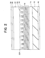
- the layer structure includes, consecutively as viewed from the bottom, an n-InP buffer layer 14, a MQW separate confinement heterostructure (MQW-SCH) active layer structure 16 having a diffraction grating 18 formed in the top portion of the MQW active layer structure 16, and a p-InP embedded layer 20 embedded in the diffraction grating 18.
- MQW-SCH MQW separate confinement heterostructure
- the MQW-SCH active layer structure 16 includes a bottom SCH layer 24 made of InGaAsP having a bandgap wavelength of 1.2 ⁇ m, a MQW layer body 26, and a top SCH layer 27, which is made of InGaAsP having a bandgap wavelength of 1.2 ⁇ m similarly to the bottom SCH layer 24.
- the MQW layer body 26 includes a plurality of (six, in this example) InGaAs QW layers 28a to 28f each having a compressive strain of 1% and a thickness of 4 nm, and a plurality of (five, in this example) barrier layers 30a to 30e, which are respectively interposed between two of the InGaAs QW layers.
- the fourth-level barrier layer 30d as viewed from the bottom, is made of AlGaInAs having a bandgap wavelength of 1.2 ⁇ m, i.e., has an A1 component therein.
- the first through third barrier layers 30a to 30c and the fifth barrier layers 30e are made of InGaAsP having a bandgap wavelength of 1.2 ⁇ m, i.e., are free from A1 component.
- the MQW layer body 26 has a peak-gain wavelength of about 1550 ⁇ m.
- the diffraction grating 18 includes a grating structure formed in the top portion of the MQW layer structure 16 and the InP embedded layer 20 embedded in the grating structure.
- the grating structure is formed in the fifth QW layer 28e, fifth barrier layer 30e, sixth QW layer 28f and the top SCH layer 27, as clearly shown in Figs . 2 and 3.
- the AlGaInAs barrier layer 30d has a considerably lower etching rate due to the A1 content thereof compared to the etching rates of the InGaAsP top SCH layer 27, the InGaAs QW layers 28 and the InGaAsP barrier layers 30a to 30c and 30e, during a dry etching process using a mixture of methane and hydrogen as an etching gas for forming the diffraction grating 18.
- the AlGaInAs barrier layer 30d functions as an etching stop layer during the etching process for forming the diffraction grating. This affords and ensures excellent in-plane uniformity of the depth of the diffraction grating 18 over the entire semiconductor wafer on which a multiple of DFB laser devices are formed.
- the p-InP embedded layer 20, MQW-SCH active layer structure 16 having therein the diffraction grating 18, and the top portion of the InP buffer layer 14 are configured as a mesa stripe having an active layer width of about 1.5 ⁇ m. Both the sides of the mesa stripe are buried with a pair of currrent blocking structures each including, consecutively as viewed from the bottom, a p-InP layer 32 and an n-InP layer 34 which form in pair a p-n junction.
- a p-InP cladding layer 22 and a heavily doped GaInAs cap layer 36 are formed on the top surfaces of the p-InP embedded layer 20 and the n-InP layer 34.
- the cap layer 36 affords an electrical contact with a metallic electrode 38.
- a Ti/Pt/Au multilayer metallic film structure is formed as a p-side electrode 38, whereas an AuGeNi metallic film is formed as an n-side electrode 40 on the bottom surface of the n-InP substrate 12.
- a high-reflection (HR) coat is formed on the rear facet of the DFB laser 10 for laser reflection, whereas a anti-reflection (AR) coat is formed on the front facet of the DFB laser 10 for laser emission.
- HR high-reflection
- AR anti-reflection
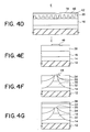
- n-InP buffer layer (or lower cladding layer) 14 and the MQW-SCH active layer structure 16 are epitaxially grown on the n-InP substrate 12 by using a MOCVD technique at a temperature of 600 °C, for example, thereby forming the layer structure.
- the MQW-SCH active layer structure 16 as shown in Fig. 4B which depicts the detail of the MQW-SCH active layer structure 16 after the growth step thereof, includes the bottom InGaAsP SCH layer 24 having a bandgap wavelength of 1.2 ⁇ m, the MQW active layer body 26 and the top InGaAsP SCH layer 27.
- the MQW active layer body 26 includes six InGaAs QW layers 28a to 28f each having a thickness of 4 nm, a fourth barrier layer 30d, as viewed from the bottom, made of AlGaInAs having a bandgap wavelength of 1.2 ⁇ m, and first through third barrier layers 30a to 30c and fifth barrier layer 30e each made of InGaAsP having a bandgap wavelength of 1.2 ⁇ m.
- a 100-nm-thick resist film for electron-beam (EB) lithography is formed by spin-coating, followed by forming a mask 42 having a pattern for the diffraction grating by using an EB lithography system.
- the mask pattern defining the diffraction grating has a spatial period of about 240 nm.
- a plurality of parallel grooves 44 are then formed in the top SCH layer 27, QW layer 28f, barrier layer 30e and the QW layer 28e which overlie the barrier layer 30d by a dry etching technique using the mask 42 having the diffraction-grating pattern, as shown in Fig. 4C, thereby forming a grating structure for the diffraction grating 18.
- This dry etching is conducted under the following conditions:
- the dry etching step using the methane/hydrogen etching gas etches the top InGaAsP SCH layer 27, InGaAsP barrier layer 30e, and the InGaAs QW layers 28e and 28f at an etching rate of about 10nm/minute and does not substantially etch the AlGaInAs barrier layer 30d due to an extremely lower etching rate thereof.
- the AlGaInAs barrier layer 30d functions as an etching stop layer, thereby stopping the etching after etching of the two QW layers 28f and 28e among the six QW layers.
- the etching is conducted for a longer time period than usual to obtain excellent in-plane uniformity over the wafer surface.
- the p-InP embedded layer 20 is then grown on the diffraction grating 18 by using a MOCVD technique to fill the groove 44 of the grating structure and is embedded the diffraction grating 18, as shown in Fig. 4D.
- This MOCVD step is conducted at a lower temperature of about 520°C to prevent the top portion of the MQW active layer 16 structure constituting the diffraction grating 18 from being deformed by excessive heat.
- a SiNx film 46 is then formed on the entire surface by using a plasma-enhanced CVD system.
- the SiNx film 46 is then patterned by using a photolithographic step and a reactive-ion etching (RIE) step to form a stripe having a width of 4 ⁇ m and extending in the direction perpendicular to the grooves 44 of the diffraction grating 18, thereby obtaining a SiNx mask pattern 48.
- Fig. 4E shows the structure taken along line E-E in Fig. 4D after the RIE step.
- the InP embedded layer 20, MQW-SCH active layer structure including the diffraction grating 18 and the upper portion of the lower cladding layer 14 are selectively etched to form a mesa stripe having a width of 1.5 ⁇ m for the MQW active layer structure 16
- the same SiNx mask 48 is used as a selective growth mask to epitaxially grow p-InP layer 32 and n-InP layer 34 as a current blocking structure on each side of the mesa stripe, whereby a so-called buried-heterostructure laser device shown in Fig. 4F is obtained.
- a 2- ⁇ m-thick p-InP cladding layer 22 and a heavily doped cap layer 36 are epitaxially grown on the n-InP layer 34 and the top of the mesa stripe.
- the n-InP substrate 12 is then polished at the bottom surface thereof to obtain a thickness of 120 ⁇ m for the n-InP substrate 12, followed by forming a multilayer metallic film including Ti/Pt/Au layers as a p-side electrode 38 on the GaInAs cap layer 36 and forming an AuGeNi metallic film as an n-side electrode 40 on the bottom surface of the n-InP substrate 12.
- An anti-reflection coat and high-reflection coat are then formed on the front end and the rear end, respectively, of the DFB laser.
- the etching stop layer is implemented by a compound semiconductor layer having therein an A1 content, which has a lower etching rate in the dry etching using a methane/hydrogen gas as an etching gas compared to compound semiconductor layers having therein no A1 content.
- the grating structure of the diffraction grating can be formed within the MQW active layer structure by incorporating the etching stop layer which also acts as a QW layer or a barrier layer in the MQW active layer structure.
- the etch selectivity between the etching stop layer and the other layers to be etched depends on the etching gas used for etching and the materials for the other layers.
- the material for the etching stop layer should be selected in consideration of the etching gas and the materials for the other layers to be etched.
- the etching for forming the diffraction grating may be a wet etching instead.
- the dry etching is more preferred because the dry etching causes little side etching and inherently achieves more excellent in-plane uniformity within the wafer surface, in a fine patterning process such as for forming the diffraction grating, compared to the wet etching.
- Samples of the DFB laser device of Fig. 1 were fabricated on a wafer and subjected to measurements of the device characteristics thereof.
- samples of DFB laser devices were selected at random from the wafer, i.e., without selecting the samples from a specific location of the wafer.
- the samples had threshold currents in the range between 9 mA and 11 mA, and operated for excellent single-mode lasing.
- the side-mode suppression ratios (SMSR) of the samples which represent the indexes or degrees of the single-mode lasing in the laser device, resided within a range as high as between 40dB and 50dB.
- the thus large SMSR itself is the feature of the gain-coupling type DFB laser devices.
- the samples selected at random from the DFB laser devices formed over the entire area of the wafer exhibited similar device characteristics, and particularly had coupling coefficients within a dispersion or variation of ⁇ 10%, which showed excellent in-plane uniformity.
- comparative samples of the conventional DFB laser device had coupling coefficients as wide a dispersion as ⁇ 20%.
- the etching stop layer is implemented by a barrier layer in the MQW active layer structure in the above embodiment, a QW layer made of AlGaInAs having a peak-gain wavelength of 1550 nm may be used as the etching stop layer. In this case, since the top surface of the etching stop QW layer constitutes a boundary between the same and the re-grown embedded layer in the diffraction grating, the re-growth process should have optimum growth conditions.
- the embedded layer may be a semiconductor layer having a composition similar to the composition of the barrier layers.
- an intrinsic gain-coupling structure for the DFB laser can be obtained.
- the diffraction grating which may be modified to have a different spatial period for the same depth, can be applied to an array of DFB lasers of a receptacle type.
Landscapes
- Physics & Mathematics (AREA)
- Engineering & Computer Science (AREA)
- Nanotechnology (AREA)
- Optics & Photonics (AREA)
- Chemical & Material Sciences (AREA)
- Crystallography & Structural Chemistry (AREA)
- Biophysics (AREA)
- Life Sciences & Earth Sciences (AREA)
- Condensed Matter Physics & Semiconductors (AREA)
- General Physics & Mathematics (AREA)
- Electromagnetism (AREA)
- Semiconductor Lasers (AREA)
- Diffracting Gratings Or Hologram Optical Elements (AREA)
- Drying Of Semiconductors (AREA)
Applications Claiming Priority (4)
| Application Number | Priority Date | Filing Date | Title |
|---|---|---|---|
| JP2001023535 | 2001-01-31 | ||
| JP2001023535 | 2001-01-31 | ||
| JP2001251110A JP2002305350A (ja) | 2001-01-31 | 2001-08-22 | 分布帰還型半導体レーザ素子及びその作製方法 |
| JP2001251110 | 2001-08-22 |
Publications (2)
| Publication Number | Publication Date |
|---|---|
| EP1233489A2 true EP1233489A2 (de) | 2002-08-21 |
| EP1233489A3 EP1233489A3 (de) | 2004-05-12 |
Family
ID=26608629
Family Applications (1)
| Application Number | Title | Priority Date | Filing Date |
|---|---|---|---|
| EP01125744A Withdrawn EP1233489A3 (de) | 2001-01-31 | 2001-10-28 | DFB Halbleiterlaservorrichtung |
Country Status (4)
| Country | Link |
|---|---|
| US (1) | US6728288B2 (de) |
| EP (1) | EP1233489A3 (de) |
| JP (1) | JP2002305350A (de) |
| CA (1) | CA2361171A1 (de) |
Families Citing this family (12)
| Publication number | Priority date | Publication date | Assignee | Title |
|---|---|---|---|---|
| US6829285B2 (en) * | 2001-09-28 | 2004-12-07 | The Furukawa Electric Co., Ltd. | Semiconductor laser device and method for effectively reducing facet reflectivity |
| US7081415B2 (en) * | 2004-02-18 | 2006-07-25 | Northrop Grumman Corporation | Method of dry plasma etching semiconductor materials |
| KR100663589B1 (ko) * | 2004-11-24 | 2007-01-02 | 삼성전자주식회사 | 분포귀환 반도체 레이저의 제조방법 |
| KR100794653B1 (ko) * | 2005-12-06 | 2008-01-14 | 한국전자통신연구원 | 분포궤환형 양자점 반도체 레이저 구조물 |
| JP2008227367A (ja) * | 2007-03-15 | 2008-09-25 | Oki Electric Ind Co Ltd | 分布帰還型半導体レーザ素子 |
| JP5205901B2 (ja) * | 2007-09-27 | 2013-06-05 | 住友電気工業株式会社 | 半導体レーザ素子の作製方法および半導体レーザ素子 |
| DE102008054217A1 (de) * | 2008-10-31 | 2010-05-06 | Osram Opto Semiconductors Gmbh | Optoelektronischer Halbleiterchip und Verfahren zur Herstellung eines optoelektronischen Halbleiterchips |
| CN102820616B (zh) * | 2012-08-31 | 2014-02-12 | 中国科学院半导体研究所 | 利用选择区域外延技术制作分布反馈激光器阵列的方法 |
| CN110535031B (zh) * | 2019-09-17 | 2024-05-31 | 全磊光电股份有限公司 | 一种高速dfb激光器外延结构及其制造方法 |
| CN110474232B (zh) * | 2019-09-17 | 2023-09-22 | 全磊光电股份有限公司 | 一种高性能dfb激光器外延结构及其制造方法 |
| CN114256737B (zh) * | 2021-12-15 | 2023-09-26 | 电子科技大学 | 一种窄线宽dfb纳米等离子体激光器及其制备方法 |
| CN115149399A (zh) * | 2022-07-25 | 2022-10-04 | 中国科学院半导体研究所 | 光栅激光器及制备方法 |
Family Cites Families (7)
| Publication number | Priority date | Publication date | Assignee | Title |
|---|---|---|---|---|
| JPS59139691A (ja) * | 1983-01-31 | 1984-08-10 | Nippon Telegr & Teleph Corp <Ntt> | 半導体レ−ザ装置 |
| JPH04218994A (ja) * | 1990-08-31 | 1992-08-10 | Toshiba Corp | 半導体発光装置 |
| EP0503473A3 (en) * | 1991-03-12 | 1992-10-28 | Texas Instruments Incorporated | Method of dry etching ina1as and ingaas lattice matched to inp |
| JP3527061B2 (ja) * | 1997-05-23 | 2004-05-17 | アルプス電気株式会社 | 分布帰還型半導体レーザ |
| JPH11233898A (ja) * | 1997-12-03 | 1999-08-27 | Canon Inc | 分布帰還型半導体レーザとその駆動方法 |
| JP2002532907A (ja) * | 1998-12-11 | 2002-10-02 | ノーテル・ネットワークス・リミテッド | 利得結合分布帰還半導体レーザ |
| JP3842976B2 (ja) * | 2000-03-17 | 2006-11-08 | 富士通株式会社 | 分布帰還型半導体レーザとその製造方法 |
-
2001
- 2001-08-22 JP JP2001251110A patent/JP2002305350A/ja active Pending
- 2001-10-28 EP EP01125744A patent/EP1233489A3/de not_active Withdrawn
- 2001-11-02 CA CA002361171A patent/CA2361171A1/en not_active Abandoned
- 2001-11-15 US US09/987,536 patent/US6728288B2/en not_active Expired - Fee Related
Also Published As
| Publication number | Publication date |
|---|---|
| US20020101896A1 (en) | 2002-08-01 |
| US6728288B2 (en) | 2004-04-27 |
| EP1233489A3 (de) | 2004-05-12 |
| CA2361171A1 (en) | 2002-07-31 |
| JP2002305350A (ja) | 2002-10-18 |
Similar Documents
| Publication | Publication Date | Title |
|---|---|---|
| US8705583B2 (en) | Semiconductor laser | |
| US8319229B2 (en) | Optical semiconductor device and method for manufacturing the same | |
| US8716044B2 (en) | Optical semiconductor device having ridge structure formed on active layer containing P-type region and its manufacture method | |
| US8273585B2 (en) | Optical semiconductor device and method for manufacturing the same | |
| JP3484394B2 (ja) | 光半導体装置およびその製造方法 | |
| JP3842976B2 (ja) | 分布帰還型半導体レーザとその製造方法 | |
| US6728288B2 (en) | DFB semiconductor laser device | |
| JP5099948B2 (ja) | 分布帰還型半導体レーザ素子 | |
| JP3745985B2 (ja) | 複素結合型の分布帰還型半導体レーザ素子 | |
| JP5143985B2 (ja) | 分布帰還型半導体レーザ素子 | |
| JP2002353559A (ja) | 半導体レーザ及びその製造方法 | |
| JP5310533B2 (ja) | 光半導体装置 | |
| US20020031152A1 (en) | Semiconductor laser device | |
| US5309465A (en) | Ridge waveguide semiconductor laser with thin active region | |
| JP2007311522A (ja) | 半導体レーザ | |
| JP2003243767A (ja) | 半導体レーザ及びこの素子を含む半導体光集積素子の製造方法 | |
| JP2882335B2 (ja) | 光半導体装置およびその製造方法 | |
| JP4599700B2 (ja) | 分布帰還型半導体レーザ | |
| JP2001274510A (ja) | 導波路型光素子及びその製造方法 | |
| JP2002324948A (ja) | 半導体レーザ及びレーザモジュール | |
| JPH0770785B2 (ja) | 分布反射型半導体レーザ | |
| JP2002057405A (ja) | 半導体レーザ装置及びその製造方法 | |
| JP3154244B2 (ja) | 半導体レーザ装置およびその製造方法 | |
| US20050078724A1 (en) | Single mode distributed feedback lasers | |
| Ohira et al. | Low-threshold distributed reflector laser consisting of wide and narrow wirelike active regions |
Legal Events
| Date | Code | Title | Description |
|---|---|---|---|
| PUAI | Public reference made under article 153(3) epc to a published international application that has entered the european phase |
Free format text: ORIGINAL CODE: 0009012 |
|
| AK | Designated contracting states |
Kind code of ref document: A2 Designated state(s): AT BE CH CY DE DK ES FI FR GB GR IE IT LI LU MC NL PT SE TR |
|
| AX | Request for extension of the european patent |
Free format text: AL;LT;LV;MK;RO;SI |
|
| PUAL | Search report despatched |
Free format text: ORIGINAL CODE: 0009013 |
|
| AK | Designated contracting states |
Kind code of ref document: A3 Designated state(s): AT BE CH CY DE DK ES FI FR GB GR IE IT LI LU MC NL PT SE TR |
|
| AX | Request for extension of the european patent |
Extension state: AL LT LV MK RO SI |
|
| AKX | Designation fees paid | ||
| REG | Reference to a national code |
Ref country code: DE Ref legal event code: 8566 |
|
| STAA | Information on the status of an ep patent application or granted ep patent |
Free format text: STATUS: THE APPLICATION IS DEEMED TO BE WITHDRAWN |
|
| 18D | Application deemed to be withdrawn |
Effective date: 20041113 |