EP1229595A2 - Procédé de fabrication d'un film conducteur transparent, procdé pour la compensation d'une region defective d'une couche semiconductrice, dispositf photovoltaique et son procédé de fabrication - Google Patents
Procédé de fabrication d'un film conducteur transparent, procdé pour la compensation d'une region defective d'une couche semiconductrice, dispositf photovoltaique et son procédé de fabrication Download PDFInfo
- Publication number
- EP1229595A2 EP1229595A2 EP02002370A EP02002370A EP1229595A2 EP 1229595 A2 EP1229595 A2 EP 1229595A2 EP 02002370 A EP02002370 A EP 02002370A EP 02002370 A EP02002370 A EP 02002370A EP 1229595 A2 EP1229595 A2 EP 1229595A2
- Authority
- EP
- European Patent Office
- Prior art keywords
- substrate
- transparent
- conductive film
- semiconductor layer
- target
- Prior art date
- Legal status (The legal status is an assumption and is not a legal conclusion. Google has not performed a legal analysis and makes no representation as to the accuracy of the status listed.)
- Withdrawn
Links
- 238000000034 method Methods 0.000 title claims abstract description 88
- 239000004065 semiconductor Substances 0.000 title claims abstract description 55
- 230000002950 deficient Effects 0.000 title claims abstract description 50
- 239000000758 substrate Substances 0.000 claims abstract description 131
- 238000004544 sputter deposition Methods 0.000 claims abstract description 40
- 239000003792 electrolyte Substances 0.000 claims description 19
- 230000015572 biosynthetic process Effects 0.000 claims description 17
- 230000007547 defect Effects 0.000 claims description 15
- 239000002253 acid Substances 0.000 claims description 7
- 239000003513 alkali Substances 0.000 claims description 7
- 150000003839 salts Chemical class 0.000 claims description 7
- 230000000452 restraining effect Effects 0.000 abstract description 2
- 239000010408 film Substances 0.000 description 118
- 229910021417 amorphous silicon Inorganic materials 0.000 description 19
- 238000005546 reactive sputtering Methods 0.000 description 17
- 238000006243 chemical reaction Methods 0.000 description 14
- 238000002161 passivation Methods 0.000 description 14
- 239000002585 base Substances 0.000 description 10
- 238000004519 manufacturing process Methods 0.000 description 9
- 238000004804 winding Methods 0.000 description 8
- XOLBLPGZBRYERU-UHFFFAOYSA-N SnO2 Inorganic materials O=[Sn]=O XOLBLPGZBRYERU-UHFFFAOYSA-N 0.000 description 7
- 230000006866 deterioration Effects 0.000 description 7
- 238000007667 floating Methods 0.000 description 7
- 230000035945 sensitivity Effects 0.000 description 7
- XLOMVQKBTHCTTD-UHFFFAOYSA-N Zinc monoxide Chemical compound [Zn]=O XLOMVQKBTHCTTD-UHFFFAOYSA-N 0.000 description 6
- 238000002834 transmittance Methods 0.000 description 5
- 229910000577 Silicon-germanium Inorganic materials 0.000 description 4
- PJXISJQVUVHSOJ-UHFFFAOYSA-N indium(III) oxide Inorganic materials [O-2].[O-2].[O-2].[In+3].[In+3] PJXISJQVUVHSOJ-UHFFFAOYSA-N 0.000 description 4
- 230000008569 process Effects 0.000 description 4
- 230000000052 comparative effect Effects 0.000 description 3
- 230000001276 controlling effect Effects 0.000 description 3
- 238000005530 etching Methods 0.000 description 3
- 230000001965 increasing effect Effects 0.000 description 3
- AMGQUBHHOARCQH-UHFFFAOYSA-N indium;oxotin Chemical compound [In].[Sn]=O AMGQUBHHOARCQH-UHFFFAOYSA-N 0.000 description 3
- 230000007246 mechanism Effects 0.000 description 3
- 238000012544 monitoring process Methods 0.000 description 3
- 239000010409 thin film Substances 0.000 description 3
- 239000011787 zinc oxide Substances 0.000 description 3
- JOYRKODLDBILNP-UHFFFAOYSA-N Ethyl urethane Chemical compound CCOC(N)=O JOYRKODLDBILNP-UHFFFAOYSA-N 0.000 description 2
- NIXOWILDQLNWCW-UHFFFAOYSA-N acrylic acid group Chemical group C(C=C)(=O)O NIXOWILDQLNWCW-UHFFFAOYSA-N 0.000 description 2
- 230000004913 activation Effects 0.000 description 2
- 239000002390 adhesive tape Substances 0.000 description 2
- 229910052782 aluminium Inorganic materials 0.000 description 2
- XAGFODPZIPBFFR-UHFFFAOYSA-N aluminium Chemical compound [Al] XAGFODPZIPBFFR-UHFFFAOYSA-N 0.000 description 2
- 239000011248 coating agent Substances 0.000 description 2
- 238000000576 coating method Methods 0.000 description 2
- 238000001816 cooling Methods 0.000 description 2
- 230000003247 decreasing effect Effects 0.000 description 2
- 238000000151 deposition Methods 0.000 description 2
- 239000000428 dust Substances 0.000 description 2
- 230000000694 effects Effects 0.000 description 2
- 238000002474 experimental method Methods 0.000 description 2
- 229910003437 indium oxide Inorganic materials 0.000 description 2
- 230000001939 inductive effect Effects 0.000 description 2
- 150000002500 ions Chemical class 0.000 description 2
- 238000001755 magnetron sputter deposition Methods 0.000 description 2
- 229920001721 polyimide Polymers 0.000 description 2
- 230000001105 regulatory effect Effects 0.000 description 2
- 239000013077 target material Substances 0.000 description 2
- 229910001887 tin oxide Inorganic materials 0.000 description 2
- XLYOFNOQVPJJNP-UHFFFAOYSA-N water Substances O XLYOFNOQVPJJNP-UHFFFAOYSA-N 0.000 description 2
- BLRPTPMANUNPDV-UHFFFAOYSA-N Silane Chemical compound [SiH4] BLRPTPMANUNPDV-UHFFFAOYSA-N 0.000 description 1
- 230000009471 action Effects 0.000 description 1
- 229910045601 alloy Inorganic materials 0.000 description 1
- 239000000956 alloy Substances 0.000 description 1
- 150000001768 cations Chemical class 0.000 description 1
- 229910021419 crystalline silicon Inorganic materials 0.000 description 1
- 230000000593 degrading effect Effects 0.000 description 1
- 230000008021 deposition Effects 0.000 description 1
- 238000001312 dry etching Methods 0.000 description 1
- 238000001978 electrochemical passivation Methods 0.000 description 1
- 238000003487 electrochemical reaction Methods 0.000 description 1
- 239000012789 electroconductive film Substances 0.000 description 1
- 238000005566 electron beam evaporation Methods 0.000 description 1
- 230000008020 evaporation Effects 0.000 description 1
- 238000001704 evaporation Methods 0.000 description 1
- 238000010438 heat treatment Methods 0.000 description 1
- 230000006872 improvement Effects 0.000 description 1
- 230000003993 interaction Effects 0.000 description 1
- 239000008204 material by function Substances 0.000 description 1
- 238000005259 measurement Methods 0.000 description 1
- 229910052751 metal Inorganic materials 0.000 description 1
- 239000002184 metal Substances 0.000 description 1
- 230000003287 optical effect Effects 0.000 description 1
- 238000010248 power generation Methods 0.000 description 1
- 239000011347 resin Substances 0.000 description 1
- 229920005989 resin Polymers 0.000 description 1
- 229910000077 silane Inorganic materials 0.000 description 1
- 238000005507 spraying Methods 0.000 description 1
- 239000010935 stainless steel Substances 0.000 description 1
- 229910001220 stainless steel Inorganic materials 0.000 description 1
- 239000000126 substance Substances 0.000 description 1
Images


Classifications
-
- H—ELECTRICITY
- H01—ELECTRIC ELEMENTS
- H01L—SEMICONDUCTOR DEVICES NOT COVERED BY CLASS H10
- H01L31/00—Semiconductor devices sensitive to infrared radiation, light, electromagnetic radiation of shorter wavelength or corpuscular radiation and specially adapted either for the conversion of the energy of such radiation into electrical energy or for the control of electrical energy by such radiation; Processes or apparatus specially adapted for the manufacture or treatment thereof or of parts thereof; Details thereof
- H01L31/02—Details
- H01L31/0224—Electrodes
- H01L31/022408—Electrodes for devices characterised by at least one potential jump barrier or surface barrier
- H01L31/022425—Electrodes for devices characterised by at least one potential jump barrier or surface barrier for solar cells
-
- H—ELECTRICITY
- H01—ELECTRIC ELEMENTS
- H01L—SEMICONDUCTOR DEVICES NOT COVERED BY CLASS H10
- H01L31/00—Semiconductor devices sensitive to infrared radiation, light, electromagnetic radiation of shorter wavelength or corpuscular radiation and specially adapted either for the conversion of the energy of such radiation into electrical energy or for the control of electrical energy by such radiation; Processes or apparatus specially adapted for the manufacture or treatment thereof or of parts thereof; Details thereof
- H01L31/02—Details
- H01L31/0224—Electrodes
- H01L31/022466—Electrodes made of transparent conductive layers, e.g. TCO, ITO layers
- H01L31/022475—Electrodes made of transparent conductive layers, e.g. TCO, ITO layers composed of indium tin oxide [ITO]
-
- Y—GENERAL TAGGING OF NEW TECHNOLOGICAL DEVELOPMENTS; GENERAL TAGGING OF CROSS-SECTIONAL TECHNOLOGIES SPANNING OVER SEVERAL SECTIONS OF THE IPC; TECHNICAL SUBJECTS COVERED BY FORMER USPC CROSS-REFERENCE ART COLLECTIONS [XRACs] AND DIGESTS
- Y02—TECHNOLOGIES OR APPLICATIONS FOR MITIGATION OR ADAPTATION AGAINST CLIMATE CHANGE
- Y02E—REDUCTION OF GREENHOUSE GAS [GHG] EMISSIONS, RELATED TO ENERGY GENERATION, TRANSMISSION OR DISTRIBUTION
- Y02E10/00—Energy generation through renewable energy sources
- Y02E10/50—Photovoltaic [PV] energy
Definitions
- the present invention relates to a transparent, conductive film forming method of forming a transparent, conductive film on a semiconductor layer stacked on a substrate, by sputtering, a semiconductor-layer defective region compensation method of compensating a defective region produced in a semiconductor layer stacked on a substrate, a photovoltaic element in which a transparent, conductive film is formed by sputtering, on a semiconductor layer stacked on a substrate, and a method of producing a photovoltaic element.
- the latter reactive sputtering method allows increase of film forming rates.
- the utilization efficiency of the target material is approximately 2.5 to 3 times higher than those of the general planar type (Kinouzairyou (Functional materials), Vol. 11, No. 3, pp. 35-41, March 1991).
- the advantages of this reactive sputtering method include saving of the target material and great decrease of production stop time for exchange of targets. Accordingly, the DC magnetron sputtering apparatus using the rotatable target is suitable for volume production.
- This reactive sputtering requires extremely narrow adequate ranges of film formation conditions, particularly, flow rates of gas; for example, where a transparent, conductive film was formed on a sheet-like substrate of a large area, it was difficult to control the film formation parameters such as evenness of sheet resistance and transmittance, discharge stability, and so on.
- the reactive sputtering method employing a plasma emission monitor (hereinafter referred to as "PEM”) is known as a method overcoming the disadvantage.
- This PEM is a device for collecting plasma emission by a collimator, guiding the emitted light through a spectroscope to a photomultiplier tube (photomultiplier), photoelectrically converting the light into an electric signal, and monitoring the state of the plasma, based on the electric signal.
- the device has a function of setting the sensitivity of the photomultiplier of the PEM at a certain value and regulating the flow rate of introduction of reactive gas so as to keep the emission intensity of the plasma constant.
- Japanese Patent Application Laid-Open No. 11-29863 discloses the technique of forming a film of ITO (Indium Tin Oxide) on a substrate.
- This technique is generally a method of setting a substrate in a film forming chamber, inducing discharge in the film forming chamber in a state in which sputter gas is introduced and reactive gas is not introduced thereinto, adjusting the sensitivity of the device for monitoring the emission intensity of the plasma such that the emission intensity of the plasma of the discharge becomes a predetermined value, and sputtering the target while controlling the introducing amount of the reactive gas so as to keep the film forming rate constant.
- a-Si amorphous silicon
- solar cells are drawing attention, because they can be produced at lower cost and have higher mass producibility than the solar cells produced using crystalline Si and others.
- the reason for it is that it is possible to use readily available gas such as silane or the like as source gas, decompose it by glow discharge, and form a deposited film of a semiconductor film or the like on a relatively inexpensive, belt-like substrate such as a metal sheet, a resin sheet, or the like.
- the output power of about 3 kW is necessary for applying the solar cells to power supply at ordinary households.
- the area in that case is 30 m 2 , and it is thus necessary to prepare the solar cells of large area. It is, however, very hard to produce the solar cells without defects over a large area because of the production steps of solar cells.
- causes of production of defects and their effect include the following; for example, in the case of the a-Si solar cell deposited on a stainless steel substrate, the substrate surface cannot be regarded as a perfectly smooth surface, but has flaws and dents, a back surface reflecting layer of uneven structure is provided on the substrate for the purpose of effective use of incident light, it is thus difficult for thin film semiconductor layers several ten nm thick such as n- or p-layers to completely cover such a surface, defects are produced by dust or the like during film formation, and so on.
- the semiconductor layers between the lower electrode and the upper electrode of the solar cell are lost because of the defects or the like to cause direct contact between the lower electrode and the upper electrode or where the semiconductor layers are not lost completely but themselves have a low resistance to cause shunts between the upper electrode and the lower electrode
- the electric current generated by light will flow through the upper electrode into the low resistant regions of the shunt portions, resulting in loss of electric current.
- Such current loss will result in decrease of open circuit voltage of the solar cell.
- the upper electrode consisting of a transparent, conductive film over the entire semiconductor surface.
- the upper electrode is a transparent, electroconductive film such as films of SnO 2 , In 2 O 3 , ITO (In 2 O 3 + SnO 2 ), and so on with excellent characteristics as to transparency to the visible light and electric conductivity.
- These transparent, conductive films are normally formed by sputtering, vacuum resistance heating evaporation, electron beam evaporation, spraying, and so on. When there exist defects in the semiconductor layers, a considerably large amount of electric current flows into the fine defects.
- the defects are located apart from a grid electrode provided on the transparent, conductive film, the resistance is high against the flow of current into the defective portions and the power loss is thus relatively small. Conversely, if the defective portions are located below the grid electrode, the defects cause greater loss of electric current.
- the defective portions in addition to the leakage of charge generated in the semiconductor layers, into the defective portions, the defective portions under existence of water produce ionic substances because of interaction with water. They gradually decrease the electric resistance at the defective portions with a lapse of operating time during use of the solar cells, whereby there appears the phenomenon of degrading the characteristics of the photoelectric conversion efficiency and others.
- the current loss can be reduced by removing the upper electrode of the transparent, conductive film at positions of the shunts.
- methods of selectively removing the upper electrode at the shunt portions there are removing techniques of immersing the solar cell in an acid, salt, or alkali electrolyte and applying a bias to the solar cell to etch the shunt portions, as disclosed in U.S. Pat. Nos. 4,451,970 and 4,464,832.
- the sheet resistance of the transparent, conductive film deposited on the semiconductor layer is considered to be preferably as low as possible. Decrease in the sheet resistance of the transparent, conductive film can decrease the series resistance of the solar cells and increase the fill factor in the current-voltage curve (I-V curve) of the solar cells. Further, the decrease in the sheet resistance of the transparent, conductive film can increase the current collection efficiency and if the grid electrode is formed by attachment of wires the number of grids can be decreased and loss of light due to shadows of wires (shadow loss) can be decreased.
- the present invention has been accomplished in view of the above problems and an object of the invention is to provide a method of forming a transparent, conductive film with excellent characteristics and high yield by sputtering, without causing the shunts or the deterioration of appearance, a defective region compensation method of a semiconductor layer, a photovoltaic element, and a method of producing a photovoltaic element.
- a transparent, conductive film forming method is a method of forming a transparent, conductive film on a semiconductor layer formed on a substrate, by sputtering, comprising applying voltages independently of each other to both a target and the substrate, respectively, and controlling a bias voltage appearing in the substrate so as to form the transparent, conductive film on only a portion except for a defective region of the semiconductor layer.
- At least one of the voltages applied to the target and the substrate is controlled such that a self bias of the substrate is -20 V to 0 V in a state in which the voltage is applied to only the target and such that a self bias of the substrate is -90 V to -30 V in a state in which the voltages are applied to both the target and the substrate, respectively, independently of each other.
- an introducing amount of a reactive gas is controlled such that a ratio of emission intensity of In during formation of the transparent, conductive film in a state in which the voltages are applied to both the target and the substrate, respectively, independently of each other to emission intensity of In during discharge in only an Ar atmosphere is within the range of 0.15 to 0.36.
- a defective region compensation method of a semiconductor layer according to the present invention is a method of compensating a defective region existing in a semiconductor layer formed on a substrate, comprising:
- a photovoltaic element producing method is a method of producing a photovoltaic element, comprising:
- a photovoltaic element producing method is a method of producing a photovoltaic element, comprising:
- a photovoltaic element according to the present invention is a photovoltaic element comprising at least a semiconductor layer and a transparent, conductive film formed on the semiconductor layer, on a substrate, the photovoltaic element being produced by the method as described above.
- a transparent, conductive film forming method is a method of forming a transparent, conductive film on a semiconductor layer formed on a substrate, by sputtering, comprising applying voltages independently of each other to a target and the substrate, respectively, so as to satisfy at least the following conditions of (1) and (2):
- a vacuum chamber of the present embodiment there are provided independent, external power supplies for both a target and a substrate facing each other, and a device for monitoring the emission intensity of the plasma (hereinafter referred to as "PEM") according to necessity.
- the sensitivity of the photomultiplier is adjusted such that the emission intensity of In during discharge in only an Ar atmosphere becomes 900, a reactive gas (O 2 ) is then introduced, and a voltage is applied from the first power supply to the target such that a self bias appearing on the substrate becomes -20 V to 0 V. Subsequent thereto, a voltage is applied from the second power supply to the substrate such that the self bias of -90 V to -30 V appears on the substrate, and then film formation is started.
- a ratio of emission intensities of In (a ratio of the emission intensity during formation of the transparent, conductive film to the emission intensity during discharge in only the Ar atmosphere (i.e., in a state without introduction of a reactive gas)) was within the range of 0.15 to 0.36.
- the voltages may be applied to both the target and the substrate from the beginning as long as the following conditions are met: the self bias of the substrate is -20 V to 0 V in a state in which the voltage is applied to only the target; and the self bias of the substrate is -90 V to -30 V in a state in which the voltages are applied to both the target and the substrate.
- the defective regions are selectively removed even if the sheet resistance of the transparent electrode film (e.g., the ITO film (indium tin oxide film)) is low.
- the transparent electrode film e.g., the ITO film (indium tin oxide film)
- Fig. 9A shows a photovoltaic element produced by the sputtering method according to the present invention
- Fig. 9B a photovoltaic element produced by the ordinary sputtering method. As shown in Figs. 9A and 9B, comparison is made between the defective regions of the two photovoltaic elements.
- Numeral 901 designates a substrate, 902 an Si layer, 903 a transparent, conductive film, 904 defective regions, 905 defective Si films, 906 defective regions (having the transparent, conductive film), and 907 portions from which the good, transparent, conductive film was removed by electrolyte passivation.
- the ITO film is uniformly deposited over both the defective regions and the non-defective regions, because the bias voltage is not applied to the substrate, different from the present invention. It was thus verified that the passivation in the electrolyte also removed even the good ITO film around the defective regions of low resistance.
- the negative charge is concentrated on the defective regions because of the application of the bias to the substrate, so that Ar ions (cations) may implement local sputtering.
- the sputtering according to the present invention causes the transparent electrode film to be anisotropically etched, whereby the transparent electrode film can be selectively removed from only the defective regions.
- the electrolytic passivation may be further carried out.
- the present invention can relieve the problem of removal of the good ITO film from the regions except for the defective regions, which arises in the ordinary electrolyte passivation.
- the photovoltaic element without deposition of the transparent, conductive film on the defective regions in the semiconductor layer is improved in the shunts of solar cell, the deterioration of appearance, etc., whereby the solar cell can be obtained with excellent characteristics and high yield.
- Fig. 1 is a cross-sectional view of a reactive sputtering apparatus using a cylindrical, rotatable target.
- a vacuum chamber 104 is comprised of a substrate feeding chamber 113, a film forming chamber 114, and a substrate winding chamber 115, the interior of each of which can be evacuated by a vacuum pump not shown.
- An elongated substrate 101 is wound on a substrate feeding roll 102, is conveyed from left to right by an unrepresented conveying means, and is wound up in proper alignment onto a substrate winding roll 103 via a steering mechanism 117.
- a cathode electrode 106 is cylindrical and a target 105 is bonded to the periphery of the cathode electrode 106.
- a magnet 107 and an unrepresented cooling means are provided inside the cathode electrode 106.
- a dc power supply 108 is connected with the vacuum chamber 104 as an anode, and the power is placed between the cathode electrode 106 and the vacuum chamber 104.
- a dc power supply 119 for applying the voltage to the substrate is also placed.
- sheath heaters are used as heater 110 and heater 111.
- the heater 110 is located on a little left side (on the substrate feeding roll 102 side) with regard to the cathode electrode 106, while the heater 111 is located just over the cathode electrode 106.
- the heater 110 is one having the electric capacity greater than that of the heater 111.
- a thickness gage 109 is an optical interference type thickness gage.
- the substrate winding roll 102 with the elongated substrate 101 wound thereon is set in the substrate feeding chamber 113.
- the elongated substrate 101 is routed in the order of the substrate feeding chamber 113, the film forming chamber 114, and the substrate winding chamber 115 to be fixed on the substrate winding roll 103, and is rolled thereon by approximately two to three turns.
- a tension is exerted on the substrate by an unrepresented tension generating mechanism.
- the elongated substrate 101 as an electroconductive substrate is electrically insulated (Japanese Patent Application Laid-Open No. 10-92766). On this occasion the insulating condition is confirmed.
- the film forming chamber 114 is evacuated to the vacuum degree of 10 -3 Pa by the unrepresented vacuum pump. Then, the Ar gas is introduced to the vacuum degree of 0.3 Pa. Further, the outputs of the heater 110 and the heater 111 are controlled. The heater 110 and the heater 111 are energized and the outputs of the heater 110 and the heater 111 are controlled so that the temperature becomes 215°C and 200°C at the positions of the respective heaters on the back surface of the elongated substrate 101. After one hour has elapsed since the energization of the heater 110 and the heater 111, the power of 1.8 kW is applied from the target dc power supply 108 to the cathode electrode 106.
- the sensitivity of the photomultiplier of the PEM is adjusted by the method disclosed in Japanese Patent Application Laid-Open No. 11-029863.
- the PEM can be the plasma emission monitor PEM04 available from ARDENNNEANLAGENTECHNIK, or the like.
- the sensitivity adjusting method is a method of inducing discharge in only the Ar gas and adjusting the gain of the photomultiplier so that the plasma emission intensity becomes 900. After the adjustment, the O 2 gas is introduced to start film formation.
- the target value of the plasma emission intensity is adjusted so that an indication of the thickness gage becomes, for example, 60 nm. This adjustment is carried out as occasion may demand.
- the self bias voltage on the substrate in this state is desirably controlled in the range of 0 to -20 V.
- the self bias voltage is set to -30 to -90 V through use of the substrate dc power supply 119.
- the transparent, conductive film is produced under the condition that the self bias voltage becomes preferably -40 to -70 V and more preferably -50 to -60 V.
- the voltage of -90 V to -30 V is applied from the second power supply to the substrate and the emission intensity ratio of In is controlled in the range of 0.15 to 0.36.
- the emission intensity ratio of In is controlled preferably in the range of 0.16 to 0.35 and more preferably in the range of 0.17 to 0.34.
- the O 2 gas, Ar gas, dc power supply 108, heater 110, and heater 111 all are stopped. Further, the conveyance of the elongated substrate 101 is terminated and after one-hour cooling, the pressure inside the vacuum chamber 104 is brought back to the atmospheric pressure. The product is then taken out.
- the present example describes a Roll to Roll sputtering apparatus of the reactive sputtering method. It is noted that the same idea can also apply similarly, irrespective of the method and apparatus, to any sputtering apparatus provided with the target and the substrate in the vacuum chamber and the independent external power supplies for applying the voltages to the target and the substrate, respectively.
- the apparatus may be provided with the PEM.
- the transparent, conductive film was formed with variation of the self bias voltage in the range of -150 V to 20 V, thereby producing solar cells.
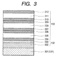
- the substrate 101 was one in which a semiconductor junction layer (of a triple cell type) 133 was provided through a reflecting layer 132 on an electroconductive base 131, as shown in Fig. 3.
- numeral 301 designates an electroconductive base, 302 an aluminum layer, 303 a zinc oxide layer, 304 an n-type a-Si layer, 305 an i-type a-SiGe layer, 306 a p-type a-Si layer, 307 an n-type a-Si layer, 308 an i-type a-SiGe layer, 309 a p-type a-Si layer, 310 an n-type a-Si layer, 311 an i-type a-Si layer, and 312 a p-type a-Si layer.
- a method of forming the transparent, conductive film will be described below according to the production procedure thereof.
- the substrate 101 wound on the substrate feeding roll 102 was mounted in the substrate feeding chamber 113, and guided via feeding fixed roller 116 and steering roller 117 to be rolled onto the substrate winding roll 103.
- a polyimide film was bonded with a double-sided adhesive tape to the surface of each roller 102, 116, 117, 103 in contact with the conductive base 131.
- the electric resistance between the conductive base 131 and the vacuum chamber 104 was measured with a tester.
- the measured resistance was of M ⁇ (megaohm) order, which assured that the substrate 101 was electrically insulated (or made in an electrically floating state).
- the interior of the vacuum chamber 104 was evacuated to the vacuum degree of 10 -3 Pa and thereafter Ar gas was introduced into the film forming chamber 114.
- the preheater 110 and heater 111 were activated and the outputs thereof were controlled so that the thermocouple not shown (immediately below the heater 111) indicated 215°C.
- the target dc power supply 108 was turned on at one hour after the activation of the preheater 110 and heater 111 and O 2 was introduced in the state of 1.8 kW. After a lapse of ten minutes, the substrate 101 was started moving.
- the voltage was applied in the range of -150 V to 20 V through use of the substrate dc power supply, thereby producing the transparent, conductive film.
- this transparent, conductive film roll was cut into 355 mm ⁇ 240 mm by a cutter, solar cells obtained were immersed in an acid, salt, or alkali electrolyte, and a bias was applied to etch shunt portions.
- the current collector electrode was further bonded and then was coated with acrylic urethane or the like, and the characteristics of the resultant solar cells were measured.
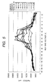
- the results of conversion efficiency characteristics were presented in Fig. 4, the results of dark shunt resistance (RshDK) in Fig. 5, and the results of Q-curve characteristics for checking the circumstances of Top current in Figs. 6A and 6B.
- the transparent, conductive film was formed with variation of the self bias voltage in the range of -150 V to 20 V, to produce solar cells.
- the substrate 101 was one in which the semiconductor junction layer (of the triple cell type) 133 was provided through the back surface reflecting layer 132 on the conductive base 131, as shown in Fig. 3. In Fig.
- numeral 301 designates an electroconductive base, 302 an aluminum layer, 303 a zinc oxide layer, 304 an n-type a-Si layer, 305 an i-type a-SiGe layer, 306 a p-type a-Si layer, 307 an n-type a-Si layer, 308 an i-type a-SiGe layer, 309 a p-type a-Si layer, 310 an n-type a-Si layer, 311 an i-type a-Si layer, and 312 a p-type a-Si layer.
- a method of forming the transparent, conductive film will be described below according to the production procedure thereof.
- the substrate 201 wound on the substrate feeding roll 202 was mounted in the substrate feeding chamber 213, and guided via the feeding fixed roller 216 and steering roller 217 to be rolled onto the substrate winding roll 203.
- a polyimide film was bonded with a double-sided adhesive tape to the surface of each roller 202, 216, 217, 203 in contact with the conductive base 131.
- Numeral 205 designates a target, 206 a cathode electrode, 207 a magnet, 209 a thickness gage, 212 a collimator, 215 a substrate winding chamber, and 219 a substrate dc power supply.
- the electric resistance between the conductive base 131 and the vacuum chamber 204 was measured with the tester.
- the measured resistance was of M ⁇ order, which assured that the substrate 201 was electrically insulated (or made in an electrically floating state).
- the interior of the vacuum chamber 204 was evacuated to the vacuum degree of 10 -3 Pa level and thereafter Ar was introduced into the film forming chamber 214.
- the preheater 210 and heater 211 were activated, and the outputs thereof were controlled so that the unrepresented thermocouple (immediately below the heater 211) indicated 215°C.
- the target dc power supply 208 was turned on and O 2 was introduced in the state of 1.8 kW. After a lapse of ten minutes, the substrate 201 was started moving.
- the voltage was applied in the range of -150 V to 20 V through use of the substrate dc power supply, to produce the transparent, conductive film.
- this transparent, conductive film roll was cut into 355 mm ⁇ 240 mm with the cutter, solar cells obtained were immersed in the acid, salt, or alkali electrolyte, and the bias was applied to etch shunt portions.
- the current collector electrode was bonded and then coated with acrylic urethane or the like, and the characteristics of the resultant solar cells were measured.
- the results of the conversion efficiency characteristics are presented in Fig. 7 and the results of the dark shunt resistance (RshDK) in Fig. 8.
- the sputtering method according to the present invention permitted use of both the reactive sputtering process and the non-reactive sputtering process.
- the above verifies that the conversion efficiency of solar cell is increased by carrying out the forming method of the transparent, conductive film according to the present invention.
- the electrolyte passivation improves RshDK further to 300 k ⁇ cm 2 . This is conceivably because the transparent, conductive film forming method according to the present invention substantially removes the ITO film from on the defective portions and the electrolyte passivation dissolves only the regions at the defective portions.
- films were formed under the following four conditions: (1) application of the substrate bias (-50 V) + within the adequate range of the In emission intensity ratio (0.2) according to the present invention; (2) application of the substrate bias (-50 V) + outside the adequate range of the In emission intensity ratio (0.39); (3) within the adequate range of the In emission intensity ratio (0.2) + application of the substrate bias (-200 V); (4) application of the substrate bias (-200 V) + outside the adequate range of the In emission intensity ratio (0.39).
- Measured values of RshDK ( ⁇ cm 2 ) of the cells made under the four conditions are presented in Table 2.
- the photovoltaic elements produced in Comparative Example 1 were further immersed in the acid, salt, or alkali electrolyte, the bias was applied thereto, and the state of the defective regions of each element was checked. An electron microscope was used for observing cross sections of the elements herein. Schematic views of the elements are presented in Figs. 9A and 9B.
- Numeral 901 designates a SUS substrate with ZnO formed thereon, 902 an Si layer, 903 a transparent, conductive film (ITO (indium tin oxide) film), 904 defective regions, 905 defective Si films, 906 defective regions (with the ITO film), and 907 portions from which the good ITO film was removed by the electrolyte passivation.
- ITO indium tin oxide
- Figs. 9A and 9B it is speculated that the execution of the sputtering method of the transparent, conductive film according to the present invention establishes the condition that potentials are applied to only the defective regions, dry etching with anisotropy (colliding direction) is implemented with Ar ions in the sputtering space, and no transparent, conductive film is deposited on the defective regions. It was also confirmed that the sputtering methods other than the present invention removed even the good transparent, conductive film because of the passivation in the electrolyte and the film became thinner (yellow).
- the present invention achieved the defective region compensation effect of the semiconductor junction layer in the sputtering space, which made it feasible to improve the solar cell characteristics based on the improvement in the transmittance, increase RshDK, decrease the deterioration of the appearance of solar cell, and increase the yield.
- the present invention is able to provide the transparent, conductive film forming method capable of forming the thin-film solar cell with excellent characteristics and high yield by sputtering, without occurrence of shunts and appearance deterioration, the defective region compensation method of a semiconductor layer, the photovoltaic element, and the production method thereof.
- a defective region compensation method of a semiconductor layer, a photovoltaic element, and a method of producing the photovoltaic element are also provided.
Landscapes
- Engineering & Computer Science (AREA)
- Physics & Mathematics (AREA)
- Condensed Matter Physics & Semiconductors (AREA)
- Electromagnetism (AREA)
- General Physics & Mathematics (AREA)
- Computer Hardware Design (AREA)
- Microelectronics & Electronic Packaging (AREA)
- Power Engineering (AREA)
- Life Sciences & Earth Sciences (AREA)
- Sustainable Development (AREA)
- Sustainable Energy (AREA)
- Photovoltaic Devices (AREA)
- Physical Vapour Deposition (AREA)
- Physical Deposition Of Substances That Are Components Of Semiconductor Devices (AREA)
- Electrodes Of Semiconductors (AREA)
- Manufacturing Of Electric Cables (AREA)
Applications Claiming Priority (2)
| Application Number | Priority Date | Filing Date | Title |
|---|---|---|---|
| JP2001025061A JP2002231984A (ja) | 2001-02-01 | 2001-02-01 | 透明導電膜の成膜方法、半導体層の欠陥領域補償方法、光起電力素子、及びその製造方法 |
| JP2001025061 | 2001-02-01 |
Publications (2)
| Publication Number | Publication Date |
|---|---|
| EP1229595A2 true EP1229595A2 (fr) | 2002-08-07 |
| EP1229595A3 EP1229595A3 (fr) | 2007-06-27 |
Family
ID=18890117
Family Applications (1)
| Application Number | Title | Priority Date | Filing Date |
|---|---|---|---|
| EP02002370A Withdrawn EP1229595A3 (fr) | 2001-02-01 | 2002-01-31 | Procédé de fabrication d'un film conducteur transparent, procdé pour la compensation d'une region defective d'une couche semiconductrice, dispositf photovoltaique et son procédé de fabrication |
Country Status (4)
| Country | Link |
|---|---|
| US (1) | US6716324B2 (fr) |
| EP (1) | EP1229595A3 (fr) |
| JP (1) | JP2002231984A (fr) |
| CN (1) | CN1194420C (fr) |
Families Citing this family (7)
| Publication number | Priority date | Publication date | Assignee | Title |
|---|---|---|---|---|
| JP2004165394A (ja) * | 2002-11-13 | 2004-06-10 | Canon Inc | 積層型光起電力素子 |
| JP2004356623A (ja) * | 2003-05-08 | 2004-12-16 | Canon Inc | 積層型光起電力素子及びその製造方法 |
| JP2004335823A (ja) * | 2003-05-09 | 2004-11-25 | Canon Inc | 光起電力素子及び光起電力素子の形成方法 |
| WO2009143136A2 (fr) * | 2008-05-19 | 2009-11-26 | University Of Toledo | Système et procédé pour un dépôt à rendement élevé de matériaux conducteurs sur des cellules solaires |
| JP2012033836A (ja) | 2010-08-03 | 2012-02-16 | Canon Inc | トップゲート型薄膜トランジスタ及びこれを備えた表示装置 |
| JP5950866B2 (ja) * | 2013-05-15 | 2016-07-13 | 株式会社神戸製鋼所 | 成膜装置及び成膜方法 |
| WO2017068942A1 (fr) * | 2015-10-21 | 2017-04-27 | 富士フイルム株式会社 | Film conducteur transparent, procédé de fabrication de film conducteur transparent, et capteur tactile |
Citations (3)
| Publication number | Priority date | Publication date | Assignee | Title |
|---|---|---|---|---|
| US4451970A (en) | 1982-10-21 | 1984-06-05 | Energy Conversion Devices, Inc. | System and method for eliminating short circuit current paths in photovoltaic devices |
| US4464832A (en) | 1981-05-14 | 1984-08-14 | Amp Incorporated | Method of making cartridge connector system |
| US6054024A (en) | 1996-09-12 | 2000-04-25 | Canon Kabushiki Kaisha | Apparatus for forming transparent conductive film by sputtering and method therefor |
Family Cites Families (6)
| Publication number | Priority date | Publication date | Assignee | Title |
|---|---|---|---|---|
| US4422916A (en) | 1981-02-12 | 1983-12-27 | Shatterproof Glass Corporation | Magnetron cathode sputtering apparatus |
| US4356073A (en) | 1981-02-12 | 1982-10-26 | Shatterproof Glass Corporation | Magnetron cathode sputtering apparatus |
| JPH05239641A (ja) * | 1992-02-26 | 1993-09-17 | Hitachi Ltd | 導電膜の形成方法とその装置、及びマグネトロンスパッタ方法とその装置、並びにインライン式マグネトロンスパッタ装置 |
| CN1072737C (zh) * | 1995-10-17 | 2001-10-10 | 佳能株式会社 | 刻蚀方法 |
| JPH1129863A (ja) | 1997-07-10 | 1999-02-02 | Canon Inc | 堆積膜製造方法 |
| US6290821B1 (en) * | 1999-07-15 | 2001-09-18 | Seagate Technology Llc | Sputter deposition utilizing pulsed cathode and substrate bias power |
-
2001
- 2001-02-01 JP JP2001025061A patent/JP2002231984A/ja not_active Withdrawn
-
2002
- 2002-01-30 US US10/058,802 patent/US6716324B2/en not_active Expired - Lifetime
- 2002-01-31 EP EP02002370A patent/EP1229595A3/fr not_active Withdrawn
- 2002-02-01 CN CNB021058997A patent/CN1194420C/zh not_active Expired - Fee Related
Patent Citations (3)
| Publication number | Priority date | Publication date | Assignee | Title |
|---|---|---|---|---|
| US4464832A (en) | 1981-05-14 | 1984-08-14 | Amp Incorporated | Method of making cartridge connector system |
| US4451970A (en) | 1982-10-21 | 1984-06-05 | Energy Conversion Devices, Inc. | System and method for eliminating short circuit current paths in photovoltaic devices |
| US6054024A (en) | 1996-09-12 | 2000-04-25 | Canon Kabushiki Kaisha | Apparatus for forming transparent conductive film by sputtering and method therefor |
Also Published As
| Publication number | Publication date |
|---|---|
| JP2002231984A (ja) | 2002-08-16 |
| CN1383217A (zh) | 2002-12-04 |
| EP1229595A3 (fr) | 2007-06-27 |
| US6716324B2 (en) | 2004-04-06 |
| CN1194420C (zh) | 2005-03-23 |
| US20020144726A1 (en) | 2002-10-10 |
Similar Documents
| Publication | Publication Date | Title |
|---|---|---|
| US5977477A (en) | Photovoltaic device | |
| JP3029178B2 (ja) | 薄膜半導体太陽電池の製造方法 | |
| US5453135A (en) | Photoelectric conversion device with improved back reflection layer | |
| US5667597A (en) | Polycrystalline silicon semiconductor having an amorphous silicon buffer layer | |
| US6054024A (en) | Apparatus for forming transparent conductive film by sputtering and method therefor | |
| JPH0566752B2 (fr) | ||
| US20040191950A1 (en) | Method of producing photovoltaic device | |
| JP2004289034A (ja) | 酸化亜鉛膜の処理方法、それを用いた光起電力素子の製造方法 | |
| US6132569A (en) | Method for producing photovoltaic element | |
| US6491808B2 (en) | Electrolytic etching method, method for producing photovoltaic element, and method for treating defect of photovoltaic element | |
| US6136162A (en) | Method and apparatus for depositing zinc oxide film and method for producing photoelectric converter device | |
| US6716324B2 (en) | Method of forming transparent, conductive film, method of compensating defective region of semiconductor layer, photovoltaic element, and method of producing photovoltaic element | |
| US6726812B1 (en) | Ion beam sputtering apparatus, method for forming a transparent and electrically conductive film, and process for the production of a semiconductor device | |
| JP3787410B2 (ja) | 堆積膜製造方法及び光起電力素子の製造方法 | |
| US6860974B2 (en) | Long-Term sputtering method | |
| JP3006701B2 (ja) | 薄膜半導体太陽電池 | |
| JPH09186351A (ja) | 光起電力素子及びその製造方法 | |
| JP2713847B2 (ja) | 薄膜太陽電池 | |
| JP2766145B2 (ja) | 薄膜半導体太陽電池の製造方法 | |
| JP2952121B2 (ja) | 光起電力素子 | |
| JP3762089B2 (ja) | 半導体装置の製造法及び光電変換装置の製造法 | |
| JPH06151908A (ja) | 太陽電池の欠陥封止方法 | |
| JPH1056192A (ja) | 光起電力素子の製造方法 | |
| JPH1140828A (ja) | 光電変換体の製造方法および製造装置 | |
| JPH11145492A (ja) | 光起電力素子の形成装置及び形成方法 |
Legal Events
| Date | Code | Title | Description |
|---|---|---|---|
| PUAI | Public reference made under article 153(3) epc to a published international application that has entered the european phase |
Free format text: ORIGINAL CODE: 0009012 |
|
| AK | Designated contracting states |
Kind code of ref document: A2 Designated state(s): AT BE CH CY DE DK ES FI FR GB GR IE IT LI LU MC NL PT SE TR |
|
| AX | Request for extension of the european patent |
Free format text: AL;LT;LV;MK;RO;SI |
|
| PUAL | Search report despatched |
Free format text: ORIGINAL CODE: 0009013 |
|
| AK | Designated contracting states |
Kind code of ref document: A3 Designated state(s): AT BE CH CY DE DK ES FI FR GB GR IE IT LI LU MC NL PT SE TR |
|
| AX | Request for extension of the european patent |
Extension state: AL LT LV MK RO SI |
|
| 17P | Request for examination filed |
Effective date: 20071227 |
|
| AKX | Designation fees paid |
Designated state(s): AT BE CH CY DE DK ES FI FR GB GR IE IT LI LU MC NL PT SE TR |
|
| 17Q | First examination report despatched |
Effective date: 20110303 |
|
| RIC1 | Information provided on ipc code assigned before grant |
Ipc: H01L 31/0224 20060101ALI20130610BHEP Ipc: H01L 31/02 20060101ALI20130610BHEP Ipc: H01L 31/18 20060101AFI20130610BHEP |
|
| STAA | Information on the status of an ep patent application or granted ep patent |
Free format text: STATUS: THE APPLICATION HAS BEEN WITHDRAWN |
|
| 18W | Application withdrawn |
Effective date: 20130930 |