EP1211727A2 - Semiconductor device having shallow trench isolation structure and manufacturing method thereof - Google Patents
Semiconductor device having shallow trench isolation structure and manufacturing method thereof Download PDFInfo
- Publication number
- EP1211727A2 EP1211727A2 EP01127962A EP01127962A EP1211727A2 EP 1211727 A2 EP1211727 A2 EP 1211727A2 EP 01127962 A EP01127962 A EP 01127962A EP 01127962 A EP01127962 A EP 01127962A EP 1211727 A2 EP1211727 A2 EP 1211727A2
- Authority
- EP
- European Patent Office
- Prior art keywords
- oxide layer
- trench
- sidewall oxide
- fet
- thickness
- Prior art date
- Legal status (The legal status is an assumption and is not a legal conclusion. Google has not performed a legal analysis and makes no representation as to the accuracy of the status listed.)
- Granted
Links
Images




Classifications
-
- H—ELECTRICITY
- H10—SEMICONDUCTOR DEVICES; ELECTRIC SOLID-STATE DEVICES NOT OTHERWISE PROVIDED FOR
- H10W—GENERIC PACKAGES, INTERCONNECTIONS, CONNECTORS OR OTHER CONSTRUCTIONAL DETAILS OF DEVICES COVERED BY CLASS H10
- H10W10/00—Isolation regions in semiconductor bodies between components of integrated devices
-
- H—ELECTRICITY
- H10—SEMICONDUCTOR DEVICES; ELECTRIC SOLID-STATE DEVICES NOT OTHERWISE PROVIDED FOR
- H10B—ELECTRONIC MEMORY DEVICES
- H10B12/00—Dynamic random access memory [DRAM] devices
-
- H—ELECTRICITY
- H10—SEMICONDUCTOR DEVICES; ELECTRIC SOLID-STATE DEVICES NOT OTHERWISE PROVIDED FOR
- H10W—GENERIC PACKAGES, INTERCONNECTIONS, CONNECTORS OR OTHER CONSTRUCTIONAL DETAILS OF DEVICES COVERED BY CLASS H10
- H10W10/00—Isolation regions in semiconductor bodies between components of integrated devices
- H10W10/01—Manufacture or treatment
-
- H—ELECTRICITY
- H10—SEMICONDUCTOR DEVICES; ELECTRIC SOLID-STATE DEVICES NOT OTHERWISE PROVIDED FOR
- H10W—GENERIC PACKAGES, INTERCONNECTIONS, CONNECTORS OR OTHER CONSTRUCTIONAL DETAILS OF DEVICES COVERED BY CLASS H10
- H10W10/00—Isolation regions in semiconductor bodies between components of integrated devices
- H10W10/01—Manufacture or treatment
- H10W10/011—Manufacture or treatment of isolation regions comprising dielectric materials
- H10W10/014—Manufacture or treatment of isolation regions comprising dielectric materials using trench refilling with dielectric materials, e.g. shallow trench isolations
- H10W10/0143—Manufacture or treatment of isolation regions comprising dielectric materials using trench refilling with dielectric materials, e.g. shallow trench isolations comprising concurrently refilling multiple trenches having different shapes or dimensions
-
- H—ELECTRICITY
- H10—SEMICONDUCTOR DEVICES; ELECTRIC SOLID-STATE DEVICES NOT OTHERWISE PROVIDED FOR
- H10W—GENERIC PACKAGES, INTERCONNECTIONS, CONNECTORS OR OTHER CONSTRUCTIONAL DETAILS OF DEVICES COVERED BY CLASS H10
- H10W10/00—Isolation regions in semiconductor bodies between components of integrated devices
- H10W10/10—Isolation regions comprising dielectric materials
- H10W10/17—Isolation regions comprising dielectric materials formed using trench refilling with dielectric materials, e.g. shallow trench isolations
Definitions
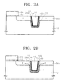
- a photo resist pattern 26 is formed by a photolithography process to expose the cell area A1.
- the thermal oxide layer 24 in the exposed cell area A1 is etched by an isotropic etching method.
- the thermal oxide layer 24 is etched, leaving a predetermined thickness thereof in the second trench T2.
- the silicon semiconductor substrate 20 is hydrophobic and thus is easily damaged by the isotropic etching. Consequently, the thermal oxide layer 24 is leftover to prevent such damage.
- reference numeral 24a denotes thermal oxide layer etched to a predetermined thickness.
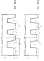
- a first sidewall oxide layer 40 is formed by thermally oxidizing the inner surfaces of the trenches T1 and T2. At this time, the first sidewall oxide layer 40 is formed to a thickness capable of preventing the generation of standby current in the P-FET in the core and periphery areas A2. That is, the first sidewall oxide layer 40 is formed to the thickness capable of preventing the penetration into the semiconductor substrate of electrons trapped in a liner which will be formed by a subsequent process, for example, to a thickness of 100 to 300 ⁇ .
- the entire sidewall oxide layer is thickly formed and is partially removed in the cell area, thereby forming the sidewall oxide layers having different thicknesses in the respective areas.
- the fourth preferred embodiment may be the same as any one of the above-described first through third embodiments in a method of manufacturing a semiconductor device having an STI structure, except the location of the STI layer.
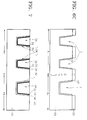
- the relatively thick first sidewall oxide layers 28 and 40 are formed in the trench T1 in the core and periphery areas requiring the P-FET and the relatively thin second sidewall oxide layers 30 and 42 are formed in the trench T2 in the cell area.
- a relatively thick first sidewall oxide layer 28 or 40 is formed in a trench T3 for defining areas between P-FETs in the core and periphery areas.
- a relatively thin second sidewall oxide layer 30 or 42 is formed in a trench T2 in the cell area as well as in a trench T4 defining other circuit devices, but not in a trench defining the P-FETs in the core and periphery areas. That is, in the fourth embodiment, the trench, in which the second sidewall oxide layer 30 or 42 is formed, may be between N-FETs, an N-FET and a P-FET, an N-FET or other circuit devices, a P-FET and other circuit devices, and other circuit devices.
Landscapes
- Semiconductor Memories (AREA)
- Element Separation (AREA)
- Metal-Oxide And Bipolar Metal-Oxide Semiconductor Integrated Circuits (AREA)
- Insulated Gate Type Field-Effect Transistor (AREA)
Abstract
Description
forming a second


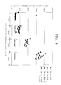
thickness of the sidewall oxide layer is 80 Å, and ○ and • represent standby current when the thickness of the sidewall oxide layer is 110 Å. Hollow symbols represent standby current measured after the P-FET has been driven for 1 hour or less and solid symbols represent standby current measured after the P-FET has been driven for 48 hours. The thickness of the sidewall oxide layer is plotted on the X-axis and standby current after burn-in is plotted on the Y-axis.
Claims (59)
- A semiconductor device having a shallow trench isolation (STI) structure, comprising:a semiconductor substrate having a first area with a first trench formed therein and a second area with a second trench formed therein;a first sidewall oxide layer formed on an inner surface of the first trench;a second sidewall oxide layer formed on an inner surface of the second trench, the second sidewall oxide layer having a thickness less than the first sidewall oxide layer;a liner formed on surfaces of the first and second sidewall oxide layers; anda dielectric material that fills the first and second trenches.
- The semiconductor device of claim 1, wherein the first area defines P-FETs and the second area defines N-FETs, an N-FET and a P-FET, an N-FET and other circuit devices, a P-FET and other circuit devices, and other circuit devices.
- The semiconductor device of claim 2, wherein the first sidewall oxide layer has a thickness capable of preventing a significant increase in standby current after burn-in in the P-FET.
- The semiconductor device of claim 3, wherein the thickness of the first sidewall oxide layer is 100 to 300 Å.
- The semiconductor device of claim 2, wherein the second sidewall oxide layer has a thickness that does not appreciably reduce a predetermined data retention time of a memory device.
- The semiconductor device of claim 5, wherein the thickness of the second sidewall oxide layer is 20 to 100 Å.
- The semiconductor device of claim 3, wherein the second sidewall oxide layer has a thickness that does not appreciably reduce a predetermined data retention time of a memory device.
- The semiconductor device of claim 7, wherein the thickness of the second sidewall oxide layer is 20 to 100 Å.
- The semiconductor device of claim 1, wherein the liner is one selected from the group consisting of a silicon nitride layer and a silicon oxynitride layer.
- The semiconductor device of claim 1, wherein the dielectric material is a high density plasma dielectric layer.
- A semiconductor device having an STI structure, comprising:a semiconductor substrate having core and periphery areas in which a P-FET and other circuit devices are formed, a cell area in which memory devices are formed, and first and second trenches for isolating devices formed in the cell area and core and periphery areas;a first sidewall oxide layer formed on an inner surface of the first trench;a second sidewall oxide layer formed on an inner surface of the second trench, the second sidewall oxide layer having a thickness less than the first sidewall oxide layer;a liner formed on surfaces of the first and second sidewall oxide layers; anda dielectric material that fills the first and second trenches.
- The semiconductor device of claim 11, wherein the first trench is formed in the core and periphery areas and the second trench is formed in the cell area.
- The semiconductor device of claim 12, wherein the first sidewall oxide layer has a thickness capable of preventing a significant increase in standby current after burn-in in the P-FET.
- The semiconductor device of claim 13, wherein the thickness of the first sidewall oxide layer is 100 to 300 Å.
- The semiconductor device of claim 12, wherein the second sidewall oxide layer has a thickness that does not appreciably reduce a predetermined data retention time of a memory device.
- The semiconductor device of claim 15, wherein the thickness of the second sidewall oxide layer is 20 to 100 Å.
- The semiconductor device of claim 13, wherein the second sidewall oxide layer has a thickness that does not appreciably reduce a predetermined data retention time of a memory device.
- The semiconductor device of claim 17, wherein the thickness of the second sidewall oxide layer is 20 to 100 Å.
- The semiconductor device of claim 11, wherein the first trench is formed in an area for defining P-FETs in the core and periphery areas and the second trench is formed in the cell area and in an area for defining N-FETs, an N-FET and a P-FET, an N-FET and other circuit devices, a P-FET and other circuit devices, and other circuit devices in the core and periphery areas.
- The semiconductor device of claim 19, wherein the first sidewall oxide layer has a thickness capable of preventing a significant increase in standby current after burn-in in the P-FET.
- The semiconductor device of claim20, wherein the thickness of the first sidewall oxide layer is 100 to 300 Å.
- The semiconductor device of claim 19, wherein the second sidewall oxide layer has a thickness that does not appreciably reduce a predetermined data retention time of a memory device.
- The semiconductor device of claim 22, wherein the thickness of the second sidewall oxide layer is 20 to 100 Å.
- The semiconductor device of claim 20, wherein the second sidewall oxide layer has a thickness that does not appreciably reduce a predetermined data retention time of a memory device.
- The semiconductor device of claim 24, wherein the thickness of the second sidewall oxide layer is 20 to 100 Å.
- The semiconductor device of claim 11, wherein the liner is one selected from the group consisting of a silicon nitride layer and a silicon oxynitride layer.
- The semiconductor device of claim 11, wherein the dielectric material is a high density plasma dielectric layer.
- A method of manufacturing a semiconductor device having an STI structure, comprising:forming a first trench and a second trench in selective areas of a semiconductor substrate;forming a first sidewall oxide layer on an inner surface of the first trench and a second sidewall oxide layer on an inner surface of the second trench, the second sidewall oxide layer having a thickness less than the first sidewall oxide layer;forming a liner on surfaces of the first and second sidewall oxide layers; andfilling the first and second trenches with a dielectric material.
- The method of claim 28, wherein the first trench defines P-FETs and the second trench defines N-FETs, an N-FET and a P-FET, an N-FET and other circuit devices, a P-FET and other circuit devices, and other circuit devices.
- The method of claim 28, wherein forming the first and second sidewall oxide layers comprises:forming an initial oxide layer on the inner surfaces of the first and second trenches;selectively removing the initial oxide layer in the second trench; andforming a first sidewall oxide layer and a second sidewall oxide layer by oxidizing the initial oxide layer in the first trench and the inner surface of the second trench.
- The method of claim 30, wherein the initial oxide layer in the second trench is removed by an isotropic etching method.
- The method of claim 30, wherein in removing the initial oxide layer in the second trench, the initial oxide layer is etched to leave a predetermined thickness thereof on the inner surface of the second trench.
- The method of claim 32, wherein the oxide layer in the second trench is removed by an isotropic etching method.
- The method of claim 30, wherein the first sidewall oxide layer is formed to a thickness capable of preventing a significant increase in standby current after burn-in in the P-FET, and the second sidewall oxide layer is formed to a thickness that does not appreciably change a predetermined data retention time of a memory device.
- The method of claim 28, wherein forming the first and second sidewall oxide layers comprises:forming the first sidewall oxide layer to a predetermined thickness on the inner walls of the first and second trenches; andforming the second sidewall oxide layer by etching the first sidewall oxide layer on the inner surface of the second trench to a predetermined thickness thereof.
- The method of claim 35, wherein the first sidewall oxide layer is formed to a thickness capable of preventing a significant increase in standby current after burn-in in the P-FET, and the second sidewall oxide layer is formed to a thickness that does not change a predetermined data retention time of a memory device.
- A method of manufacturing a semiconductor device having an STI structure, comprising:providing a semiconductor substrate having core and periphery areas in which a P-FET and other circuit devices are formed, and a cell area in which a memory device is formed;forming a first trench and a second trench in selective portions of the core area, the periphery area, and cell area of the semiconductor substrate;forming an initial oxide layer on inner surfaces of the first and second trenches;removing the initial oxide layer in the second trench;forming first and second sidewall oxide layers on the inner surfaces of the first and second trenches by oxidizing the initial oxide layer in the first trench and the inner surface of the second trench, the second sidewall oxide layer having a thickness less than the first sidewall oxide layer;forming a liner on surfaces of the first and second sidewall oxide layers; andfilling the first and second trenches with a dielectric material.
- The method of claim 37, wherein the initial oxide layer is formed by thermally oxidizing the inner surfaces of the first and second trenches.
- The method of claim 38, wherein removing the initial oxide layer in the second trench comprises:forming a photo resist pattern over the semiconductor substrate to expose the second trench;removing the initial oxide layer in the exposed second trench by an isotropic etching method; andremoving the photo resist pattern.
- The method of claim 39, wherein the initial oxide layer in the exposed second trench is removed by the isotropic etching method to leave a predetermined thickness thereof in the second trench.
- The method of claim 39, wherein the first trench is formed in the core and periphery areas and the second trench is formed in the cell area.
- The method of claim 39, wherein the first trench is formed in an area for defining P-FETs in the core and periphery areas and the second trench is formed in the cell area and in an area for defining N-FETs, an N-FET and a P-FET, an N-FET and other circuit devices, and a P-FET and other circuit devices, and other circuit devices in the core and periphery areas.
- The method of claim 41, wherein the first sidewall oxide layer in the first trench is formed to a thickness capable of preventing a significant increase in standby current after burn-in in the P-FET, and the second sidewall oxide layer is formed to a thickness that does not appreciably reduce a predetermined data retention time of a memory device.
- The method of claim 42, wherein the first sidewall oxide layer in the first trench is formed to a thickness capable of preventing a significant increase in standby current after burn-in in the P-FET, and the second sidewall oxide layer is formed to a thickness that does not appreciably reduce a predetermined data retention time of a memory device.
- The method of claim 37, wherein the liner is one selected from the group consisting of a silicon nitride layer and a silicon oxynitride layer.
- The method of claim 37, wherein filling the first and second trenches with a dielectric material comprises:forming an dielectric material to fully fill the first and second trenches; andplanarizing the dielectric material to expose the semiconductor substrate surface.
- The method of claim 46, wherein the dielectric material is a high density plasma oxide layer.
- A method of manufacturing a semiconductor device having an STI structure, comprising:providing a semiconductor substrate having core and periphery areas in which a P-FET and other circuit devices are formed, and a cell area in which a memory device is formed;forming a first trench and a second trench in selective portions of the core area, the periphery area and the cell area of the semiconductor substrate;forming a first sidewall oxide layer to a predetermined thickness on inner surfaces of the first and second trenches;forming a second sidewall oxide layer by etching the first sidewall oxide layer in the second trench to a predetermined thickness;forming a liner on surfaces of the first and second sidewall oxide layers; andfilling the first and second trenches with a dielectric material.
- The method of claim 48, wherein the first sidewall oxide layer is formed by thermally oxidizing the inner surface of the first and second trenches.
- The method of claim 49, wherein etching the first sidewall oxide layer in the second trench to a predetermined thickness comprises:forming a photo resist pattern over the semiconductor substrate to expose the second trench;etching the first sidewall oxide layer in the second trench to a predetermined thickness; andremoving the photo resist pattern.
- The method of claim 50, wherein the first trench is formed in the core and periphery areas and the second trench is formed in the cell area.
- The method of claim 51, wherein the first sidewall oxide layer in the first trench is formed to a thickness capable of preventing a significant increase in standby current after burn-in in the P-FET, and the second sidewall oxide layer is formed to a thickness that does not appreciably reduce a predetermined data retention time of a memory device.
- The method of claim 50, wherein the first trench is formed in an area for diving P-FETs in the core and periphery areas and the second trench is formed in the cell area and in an area for diving N-FETs, an N-FET and a P-FET, an N-FET and other circuit devices, and a P-FET and other circuit devices, and other circuit devices in the core and periphery areas.
- The method of claim 53, wherein the first sidewall oxide layer in the first trench is formed to a thickness capable of preventing a significant increase in standby current after burn-in in the P-FET, and the second sidewall oxide layer is formed to a thickness that does not appreciably reduce a predetermined data retention time of a memory device.
- The method of claim 48, wherein the liner is one selected from the group consisting of a silicon nitride layer and a silicon oxynitride layer.
- The method of claim 48, wherein filling the first and second trenches with a dielectric material comprises:forming a dielectric material to fully fill the first and second trenches; andplanarizing the dielectric material to expose the semiconductor substrate surface.
- The method of claim 56, wherein the dielectric material is a high density plasma oxide layer.
- A semiconductor device having a shallow trench isolation (STI) structure, comprising:a semiconductor substrate having a first area with a first trench formed therein and a second area with a second trench formed therein;a first sidewall oxide layer formed on an inner surface of the first trench;a second sidewall oxide layer formed on an inner surface of the second trench, the second sidewall oxide layer having a thickness less than the first sidewall oxide layer; anda dielectric material that fills the first and second trenches.
- The semiconductor device of claim 1, wherein the first area includes P-FETs and the second area includes N-FETs, an N-FET and a P-FET, an N-FET and other circuit devices, a P-FET and other circuit devices, and other circuit devices.
Applications Claiming Priority (2)
| Application Number | Priority Date | Filing Date | Title |
|---|---|---|---|
| KR2000072600 | 2000-12-01 | ||
| KR1020000072600A KR100346842B1 (en) | 2000-12-01 | 2000-12-01 | Semiconductor device having shallow trench isolation structure and method for manufacturing the same |
Publications (3)
| Publication Number | Publication Date |
|---|---|
| EP1211727A2 true EP1211727A2 (en) | 2002-06-05 |
| EP1211727A3 EP1211727A3 (en) | 2003-09-03 |
| EP1211727B1 EP1211727B1 (en) | 2006-11-08 |
Family
ID=19702580
Family Applications (1)
| Application Number | Title | Priority Date | Filing Date |
|---|---|---|---|
| EP01127962A Expired - Lifetime EP1211727B1 (en) | 2000-12-01 | 2001-11-23 | Manufacturing method for a semiconductor device having shallow trench isolation structure |
Country Status (7)
| Country | Link |
|---|---|
| US (2) | US6486517B2 (en) |
| EP (1) | EP1211727B1 (en) |
| JP (1) | JP4072335B2 (en) |
| KR (1) | KR100346842B1 (en) |
| CN (1) | CN1169208C (en) |
| DE (1) | DE60124369T2 (en) |
| TW (1) | TW527685B (en) |
Cited By (2)
| Publication number | Priority date | Publication date | Assignee | Title |
|---|---|---|---|---|
| EP1394852A3 (en) * | 2002-08-30 | 2009-03-04 | Fujitsu Microelectronics Limited | Semiconductor device and method of fabricating the same |
| US9331144B2 (en) | 2012-09-04 | 2016-05-03 | Ps4 Luxco S.A.R.L. | Semiconductor device and method for producing the same |
Families Citing this family (42)
| Publication number | Priority date | Publication date | Assignee | Title |
|---|---|---|---|---|
| KR100413830B1 (en) * | 2001-04-30 | 2003-12-31 | 삼성전자주식회사 | Semiconductor device having trench isolation structure and method of fabricating the same |
| JP4672197B2 (en) * | 2001-07-04 | 2011-04-20 | 株式会社東芝 | Manufacturing method of semiconductor memory device |
| KR100426484B1 (en) * | 2001-12-22 | 2004-04-14 | 주식회사 하이닉스반도체 | Flash memory cell and method of manufacturing the same |
| DE10210434B4 (en) * | 2002-03-09 | 2007-12-27 | Infineon Technologies Ag | A method for generating a shallow trench isolation in a semiconductor device and use of such a method |
| JP2004047599A (en) * | 2002-07-10 | 2004-02-12 | Renesas Technology Corp | Semiconductor device and method of manufacturing the same |
| US6828211B2 (en) * | 2002-10-01 | 2004-12-07 | Taiwan Semiconductor Manufacturing Co., Ltd. | Shallow trench filled with two or more dielectrics for isolation and coupling or for stress control |
| KR100632664B1 (en) * | 2002-12-12 | 2006-10-11 | 주식회사 하이닉스반도체 | Device Separator Formation Method of Semiconductor Device |
| US6949445B2 (en) * | 2003-03-12 | 2005-09-27 | Micron Technology, Inc. | Method of forming angled implant for trench isolation |
| US7141468B2 (en) * | 2003-10-27 | 2006-11-28 | Texas Instruments Incorporated | Application of different isolation schemes for logic and embedded memory |
| US7364962B1 (en) * | 2004-02-02 | 2008-04-29 | Advanced Micro Devices, Inc. | Shallow trench isolation process utilizing differential liners |
| JP2005251973A (en) * | 2004-03-04 | 2005-09-15 | Fujitsu Ltd | Semiconductor device manufacturing method and semiconductor device |
| US7091106B2 (en) * | 2004-03-04 | 2006-08-15 | Advanced Micro Devices, Inc. | Method of reducing STI divot formation during semiconductor device fabrication |
| JP2005286256A (en) * | 2004-03-31 | 2005-10-13 | Nec Electronics Corp | Semiconductor device and manufacturing method thereof |
| KR100519801B1 (en) * | 2004-04-26 | 2005-10-10 | 삼성전자주식회사 | Semiconductor devices having a nod contact plug surrounded by a stress buffer spacer and methods of fabricating the same |
| KR20060001196A (en) * | 2004-06-30 | 2006-01-06 | 주식회사 하이닉스반도체 | Device Separator Formation Method of Semiconductor Device |
| KR100546161B1 (en) * | 2004-07-13 | 2006-01-24 | 주식회사 하이닉스반도체 | Device Separation Method of Semiconductor Device |
| KR100702775B1 (en) * | 2005-05-03 | 2007-04-03 | 주식회사 하이닉스반도체 | Device Separating Method of Semiconductor Device |
| KR100695868B1 (en) * | 2005-06-23 | 2007-03-19 | 삼성전자주식회사 | A device isolation film, a method of manufacturing the same, a semiconductor device having the same and a method of manufacturing the same |
| JP2007048941A (en) * | 2005-08-10 | 2007-02-22 | Fujitsu Ltd | Manufacturing method of semiconductor device |
| KR100746223B1 (en) * | 2005-09-09 | 2007-08-03 | 삼성전자주식회사 | Trench device isolation method for semiconductor devices |
| US8501632B2 (en) * | 2005-12-20 | 2013-08-06 | Infineon Technologies Ag | Methods of fabricating isolation regions of semiconductor devices and structures thereof |
| US20070200196A1 (en) * | 2006-02-24 | 2007-08-30 | Lattice Semiconductor Corporation | Shallow trench isolation (STI) devices and processes |
| US8936995B2 (en) | 2006-03-01 | 2015-01-20 | Infineon Technologies Ag | Methods of fabricating isolation regions of semiconductor devices and structures thereof |
| US7811935B2 (en) | 2006-03-07 | 2010-10-12 | Micron Technology, Inc. | Isolation regions and their formation |
| US7563690B2 (en) * | 2006-03-28 | 2009-07-21 | Macronix International Co., Ltd. | Method for forming shallow trench isolation region |
| US20070267715A1 (en) * | 2006-05-18 | 2007-11-22 | Sunil Mehta | Shallow trench isolation (STI) with trench liner of increased thickness |
| KR100801739B1 (en) * | 2006-06-28 | 2008-02-11 | 주식회사 하이닉스반도체 | Trench isolation film formation method for semiconductor devices |
| KR100831676B1 (en) * | 2006-06-30 | 2008-05-22 | 주식회사 하이닉스반도체 | Device Separation Method of Semiconductor Device |
| JP2008060266A (en) | 2006-08-30 | 2008-03-13 | Oki Electric Ind Co Ltd | Method of forming element isolation film and nonvolatile semiconductor memory |
| US20090200635A1 (en) * | 2008-02-12 | 2009-08-13 | Viktor Koldiaev | Integrated Circuit Having Electrical Isolation Regions, Mask Technology and Method of Manufacturing Same |
| CN101989599B (en) * | 2009-08-03 | 2012-06-20 | 中芯国际集成电路制造(上海)有限公司 | Semiconductor device with shallow trench isolation structure and manufacturing process thereof |
| JP2011171638A (en) * | 2010-02-22 | 2011-09-01 | Oki Semiconductor Co Ltd | Method of manufacturing semiconductor device |
| KR101890818B1 (en) | 2012-03-26 | 2018-08-22 | 에스케이하이닉스 주식회사 | Semiconductor device with isolation layer, electromagnetic device having the same and method for fabriacting the same |
| US9006080B2 (en) * | 2013-03-12 | 2015-04-14 | Taiwan Semiconductor Manufacturing Company, Ltd. | Varied STI liners for isolation structures in image sensing devices |
| US9196728B2 (en) * | 2013-12-31 | 2015-11-24 | Texas Instruments Incorporated | LDMOS CHC reliability |
| KR102185282B1 (en) | 2014-01-06 | 2020-12-01 | 삼성전자 주식회사 | Semiconductor device having positive fixed charge containing layer |
| CN103871953B (en) * | 2014-03-20 | 2017-01-04 | 上海华力微电子有限公司 | A kind of shallow groove filling method |
| KR102246280B1 (en) * | 2014-03-26 | 2021-04-29 | 에스케이하이닉스 주식회사 | Semiconductor device and method for fabricating the same |
| CN104051321A (en) * | 2014-04-22 | 2014-09-17 | 上海华力微电子有限公司 | Method for preparing shallow trench isolation structure |
| KR102150942B1 (en) | 2014-12-01 | 2020-09-03 | 삼성전자주식회사 | Semiconductor device including fin FET |
| JP6623772B2 (en) * | 2016-01-13 | 2019-12-25 | 富士電機株式会社 | Method for manufacturing silicon carbide semiconductor device |
| US11881428B2 (en) | 2021-01-05 | 2024-01-23 | Changxin Memory Technologies, Inc. | Semiconductor structure and manufacturing method thereof |
Family Cites Families (18)
| Publication number | Priority date | Publication date | Assignee | Title |
|---|---|---|---|---|
| US4729006A (en) * | 1986-03-17 | 1988-03-01 | International Business Machines Corporation | Sidewall spacers for CMOS circuit stress relief/isolation and method for making |
| US4952524A (en) * | 1989-05-05 | 1990-08-28 | At&T Bell Laboratories | Semiconductor device manufacture including trench formation |
| JPH07176606A (en) * | 1993-12-21 | 1995-07-14 | Toshiba Corp | Semiconductor device and manufacturing method thereof |
| US5447884A (en) * | 1994-06-29 | 1995-09-05 | International Business Machines Corporation | Shallow trench isolation with thin nitride liner |
| US5643823A (en) * | 1995-09-21 | 1997-07-01 | Siemens Aktiengesellschaft | Application of thin crystalline Si3 N4 liners in shallow trench isolation (STI) structures |
| KR0172262B1 (en) * | 1995-12-30 | 1999-02-01 | 김주용 | Method of fabricating semiconductor device |
| US5851900A (en) * | 1997-04-28 | 1998-12-22 | Mosel Vitelic Inc. | Method of manufacturing a shallow trench isolation for a semiconductor device |
| US5854114A (en) * | 1997-10-09 | 1998-12-29 | Advanced Micro Devices, Inc. | Data retention of EEPROM cell with shallow trench isolation using thicker liner oxide |
| US6306725B1 (en) * | 1997-11-19 | 2001-10-23 | Texas Instruments Incorporated | In-situ liner for isolation trench side walls and method |
| JPH11220017A (en) * | 1998-01-30 | 1999-08-10 | Mitsubishi Electric Corp | Semiconductor device and manufacturing method thereof |
| US6074903A (en) * | 1998-06-16 | 2000-06-13 | Siemens Aktiengesellschaft | Method for forming electrical isolation for semiconductor devices |
| US5960276A (en) * | 1998-09-28 | 1999-09-28 | Taiwan Semiconductor Manufacturing Company, Ltd. | Using an extra boron implant to improve the NMOS reverse narrow width effect in shallow trench isolation process |
| KR100292616B1 (en) * | 1998-10-09 | 2001-07-12 | 윤종용 | Manufacturing method of trench isolation |
| TW396520B (en) * | 1998-10-30 | 2000-07-01 | United Microelectronics Corp | Process for shallow trench isolation |
| US6180467B1 (en) * | 1998-12-15 | 2001-01-30 | United Microelectronics Corp. | Method of fabricating shallow trench isolation |
| US5981325A (en) * | 1999-04-26 | 1999-11-09 | United Semiconductor Corp. | Method for manufacturing CMOS |
| KR100346845B1 (en) * | 2000-12-16 | 2002-08-03 | 삼성전자 주식회사 | Method for forming shallow trench isolation in semiconductor device |
| KR100378190B1 (en) * | 2000-12-28 | 2003-03-29 | 삼성전자주식회사 | Method for fabricating trench isolation having sidewall oxide layers with a different thickness |
-
2000
- 2000-12-01 KR KR1020000072600A patent/KR100346842B1/en not_active Expired - Fee Related
-
2001
- 2001-11-23 DE DE60124369T patent/DE60124369T2/en not_active Expired - Lifetime
- 2001-11-23 EP EP01127962A patent/EP1211727B1/en not_active Expired - Lifetime
- 2001-11-27 TW TW090129250A patent/TW527685B/en not_active IP Right Cessation
- 2001-11-29 JP JP2001365202A patent/JP4072335B2/en not_active Expired - Fee Related
- 2001-11-29 US US09/998,018 patent/US6486517B2/en not_active Expired - Lifetime
- 2001-11-30 CN CNB011396520A patent/CN1169208C/en not_active Expired - Lifetime
-
2002
- 2002-09-25 US US10/255,526 patent/US6656783B2/en not_active Expired - Lifetime
Cited By (2)
| Publication number | Priority date | Publication date | Assignee | Title |
|---|---|---|---|---|
| EP1394852A3 (en) * | 2002-08-30 | 2009-03-04 | Fujitsu Microelectronics Limited | Semiconductor device and method of fabricating the same |
| US9331144B2 (en) | 2012-09-04 | 2016-05-03 | Ps4 Luxco S.A.R.L. | Semiconductor device and method for producing the same |
Also Published As
| Publication number | Publication date |
|---|---|
| JP4072335B2 (en) | 2008-04-09 |
| EP1211727B1 (en) | 2006-11-08 |
| KR20020043123A (en) | 2002-06-08 |
| CN1356722A (en) | 2002-07-03 |
| TW527685B (en) | 2003-04-11 |
| JP2002222855A (en) | 2002-08-09 |
| US6656783B2 (en) | 2003-12-02 |
| US20030030076A1 (en) | 2003-02-13 |
| KR100346842B1 (en) | 2002-08-03 |
| US6486517B2 (en) | 2002-11-26 |
| EP1211727A3 (en) | 2003-09-03 |
| CN1169208C (en) | 2004-09-29 |
| US20020100953A1 (en) | 2002-08-01 |
| DE60124369T2 (en) | 2007-10-04 |
| DE60124369D1 (en) | 2006-12-21 |
Similar Documents
| Publication | Publication Date | Title |
|---|---|---|
| US6656783B2 (en) | Semiconductor device having shallow trench isolation structure and manufacturing method thereof | |
| US6482715B2 (en) | Method of forming shallow trench isolation layer in semiconductor device | |
| US6642125B2 (en) | Integrated circuits having adjacent P-type doped regions having shallow trench isolation structures without liner layers therein therebetween and methods of forming same | |
| US6670689B2 (en) | Semiconductor device having shallow trench isolation structure | |
| US8546268B2 (en) | Manufacturing integrated circuit components having multiple gate oxidations | |
| US20020033516A1 (en) | Shallow trench isolation type semiconductor device and method of manufacturing the same | |
| US6333242B1 (en) | Method of fabricating semiconductor device without having grooves at edge portions of STI | |
| JP2003197734A (en) | Method for forming element isolation film of semiconductor device | |
| KR101025731B1 (en) | A device isolation film for a semiconductor device including a liner nitride film and a method of manufacturing the same | |
| KR100289663B1 (en) | Device Separator Formation Method of Semiconductor Device | |
| US20090170276A1 (en) | Method of Forming Trench of Semiconductor Device | |
| KR100839528B1 (en) | A semiconductor device having a trench type isolation film and a manufacturing method therefor | |
| KR20050052007A (en) | Semiconductor device with dual wall oxide and method for making the same | |
| KR20050052006A (en) | Semiconductor device with trench type isolation and method for making the same | |
| KR100500943B1 (en) | Method for protecting moat in semiconductor device with selective silicon recess | |
| KR101022672B1 (en) | Semiconductor device having trench type device isolation and manufacturing method thereof | |
| KR20050067562A (en) | Semiconductor device with trench type isolation and method for making the same | |
| KR20060133690A (en) | Non-volatile memory device manufacturing method | |
| KR20020023460A (en) | Isolating method of semiconductor device | |
| KR20050010251A (en) | A method for forming a field oxide of semiconductor device | |
| KR20050104080A (en) | Isolation in semiconductor and method for manufacturing the same | |
| KR20050002070A (en) | Fabricating method for trench isoaltion layer using pad polysilicon instead of pad nitride | |
| KR20060040124A (en) | Semiconductor device manufacturing method |
Legal Events
| Date | Code | Title | Description |
|---|---|---|---|
| PUAI | Public reference made under article 153(3) epc to a published international application that has entered the european phase |
Free format text: ORIGINAL CODE: 0009012 |
|
| 17P | Request for examination filed |
Effective date: 20011123 |
|
| AK | Designated contracting states |
Kind code of ref document: A2 Designated state(s): AT BE CH CY DE DK ES FI FR GB GR IE IT LI LU MC NL PT SE TR |
|
| AX | Request for extension of the european patent |
Free format text: AL;LT;LV;MK;RO;SI |
|
| PUAL | Search report despatched |
Free format text: ORIGINAL CODE: 0009013 |
|
| AK | Designated contracting states |
Kind code of ref document: A3 Designated state(s): AT BE CH CY DE DK ES FI FR GB GR IE IT LI LU MC NL PT SE TR |
|
| AX | Request for extension of the european patent |
Extension state: AL LT LV MK RO SI |
|
| RIC1 | Information provided on ipc code assigned before grant |
Ipc: 7H 01L 21/8234 B Ipc: 7H 01L 21/762 A |
|
| AKX | Designation fees paid |
Designated state(s): DE FR GB |
|
| 17Q | First examination report despatched |
Effective date: 20040617 |
|
| GRAP | Despatch of communication of intention to grant a patent |
Free format text: ORIGINAL CODE: EPIDOSNIGR1 |
|
| RTI1 | Title (correction) |
Free format text: MANUFACTURING METHOD FOR A SEMICONDUCTOR DEVICE HAVING SHALLOW TRENCH ISOLATION STRUCTURE |
|
| GRAS | Grant fee paid |
Free format text: ORIGINAL CODE: EPIDOSNIGR3 |
|
| GRAA | (expected) grant |
Free format text: ORIGINAL CODE: 0009210 |
|
| AK | Designated contracting states |
Kind code of ref document: B1 Designated state(s): DE FR GB |
|
| REG | Reference to a national code |
Ref country code: GB Ref legal event code: FG4D |
|
| REF | Corresponds to: |
Ref document number: 60124369 Country of ref document: DE Date of ref document: 20061221 Kind code of ref document: P |
|
| ET | Fr: translation filed | ||
| PLBE | No opposition filed within time limit |
Free format text: ORIGINAL CODE: 0009261 |
|
| STAA | Information on the status of an ep patent application or granted ep patent |
Free format text: STATUS: NO OPPOSITION FILED WITHIN TIME LIMIT |
|
| 26N | No opposition filed |
Effective date: 20070809 |
|
| REG | Reference to a national code |
Ref country code: FR Ref legal event code: PLFP Year of fee payment: 15 |
|
| REG | Reference to a national code |
Ref country code: FR Ref legal event code: PLFP Year of fee payment: 16 |
|
| REG | Reference to a national code |
Ref country code: FR Ref legal event code: PLFP Year of fee payment: 17 |
|
| REG | Reference to a national code |
Ref country code: FR Ref legal event code: PLFP Year of fee payment: 18 |
|
| PGFP | Annual fee paid to national office [announced via postgrant information from national office to epo] |
Ref country code: DE Payment date: 20201020 Year of fee payment: 20 Ref country code: FR Payment date: 20201021 Year of fee payment: 20 Ref country code: GB Payment date: 20201021 Year of fee payment: 20 |
|
| REG | Reference to a national code |
Ref country code: DE Ref legal event code: R071 Ref document number: 60124369 Country of ref document: DE |
|
| REG | Reference to a national code |
Ref country code: GB Ref legal event code: PE20 Expiry date: 20211122 |
|
| PG25 | Lapsed in a contracting state [announced via postgrant information from national office to epo] |
Ref country code: GB Free format text: LAPSE BECAUSE OF EXPIRATION OF PROTECTION Effective date: 20211122 |