EP1207554A1 - Electronic part - Google Patents
Electronic part Download PDFInfo
- Publication number
- EP1207554A1 EP1207554A1 EP00942439A EP00942439A EP1207554A1 EP 1207554 A1 EP1207554 A1 EP 1207554A1 EP 00942439 A EP00942439 A EP 00942439A EP 00942439 A EP00942439 A EP 00942439A EP 1207554 A1 EP1207554 A1 EP 1207554A1
- Authority
- EP
- European Patent Office
- Prior art keywords
- leads
- electronic component
- side surfaces
- island
- connecting portion
- Prior art date
- Legal status (The legal status is an assumption and is not a legal conclusion. Google has not performed a legal analysis and makes no representation as to the accuracy of the status listed.)
- Withdrawn
Links
Images





Classifications
-
- H—ELECTRICITY
- H10—SEMICONDUCTOR DEVICES; ELECTRIC SOLID-STATE DEVICES NOT OTHERWISE PROVIDED FOR
- H10W—GENERIC PACKAGES, INTERCONNECTIONS, CONNECTORS OR OTHER CONSTRUCTIONAL DETAILS OF DEVICES COVERED BY CLASS H10
- H10W44/00—Electrical arrangements for controlling or matching impedance
-
- H—ELECTRICITY
- H10—SEMICONDUCTOR DEVICES; ELECTRIC SOLID-STATE DEVICES NOT OTHERWISE PROVIDED FOR
- H10W—GENERIC PACKAGES, INTERCONNECTIONS, CONNECTORS OR OTHER CONSTRUCTIONAL DETAILS OF DEVICES COVERED BY CLASS H10
- H10W70/00—Package substrates; Interposers; Redistribution layers [RDL]
- H10W70/40—Leadframes
- H10W70/421—Shapes or dispositions
-
- H—ELECTRICITY
- H10—SEMICONDUCTOR DEVICES; ELECTRIC SOLID-STATE DEVICES NOT OTHERWISE PROVIDED FOR
- H10W—GENERIC PACKAGES, INTERCONNECTIONS, CONNECTORS OR OTHER CONSTRUCTIONAL DETAILS OF DEVICES COVERED BY CLASS H10
- H10W72/00—Interconnections or connectors in packages
- H10W72/071—Connecting or disconnecting
- H10W72/075—Connecting or disconnecting of bond wires
-
- H—ELECTRICITY
- H10—SEMICONDUCTOR DEVICES; ELECTRIC SOLID-STATE DEVICES NOT OTHERWISE PROVIDED FOR
- H10W—GENERIC PACKAGES, INTERCONNECTIONS, CONNECTORS OR OTHER CONSTRUCTIONAL DETAILS OF DEVICES COVERED BY CLASS H10
- H10W72/00—Interconnections or connectors in packages
- H10W72/50—Bond wires
- H10W72/531—Shapes of wire connectors
- H10W72/536—Shapes of wire connectors the connected ends being ball-shaped
-
- H—ELECTRICITY
- H10—SEMICONDUCTOR DEVICES; ELECTRIC SOLID-STATE DEVICES NOT OTHERWISE PROVIDED FOR
- H10W—GENERIC PACKAGES, INTERCONNECTIONS, CONNECTORS OR OTHER CONSTRUCTIONAL DETAILS OF DEVICES COVERED BY CLASS H10
- H10W72/00—Interconnections or connectors in packages
- H10W72/50—Bond wires
- H10W72/531—Shapes of wire connectors
- H10W72/5363—Shapes of wire connectors the connected ends being wedge-shaped
-
- H—ELECTRICITY
- H10—SEMICONDUCTOR DEVICES; ELECTRIC SOLID-STATE DEVICES NOT OTHERWISE PROVIDED FOR
- H10W—GENERIC PACKAGES, INTERCONNECTIONS, CONNECTORS OR OTHER CONSTRUCTIONAL DETAILS OF DEVICES COVERED BY CLASS H10
- H10W72/00—Interconnections or connectors in packages
- H10W72/90—Bond pads, in general
- H10W72/951—Materials of bond pads
-
- H—ELECTRICITY
- H10—SEMICONDUCTOR DEVICES; ELECTRIC SOLID-STATE DEVICES NOT OTHERWISE PROVIDED FOR
- H10W—GENERIC PACKAGES, INTERCONNECTIONS, CONNECTORS OR OTHER CONSTRUCTIONAL DETAILS OF DEVICES COVERED BY CLASS H10
- H10W74/00—Encapsulations, e.g. protective coatings
-
- H—ELECTRICITY
- H10—SEMICONDUCTOR DEVICES; ELECTRIC SOLID-STATE DEVICES NOT OTHERWISE PROVIDED FOR
- H10W—GENERIC PACKAGES, INTERCONNECTIONS, CONNECTORS OR OTHER CONSTRUCTIONAL DETAILS OF DEVICES COVERED BY CLASS H10
- H10W90/00—Package configurations
- H10W90/701—Package configurations characterised by the relative positions of pads or connectors relative to package parts
- H10W90/751—Package configurations characterised by the relative positions of pads or connectors relative to package parts of bond wires
- H10W90/756—Package configurations characterised by the relative positions of pads or connectors relative to package parts of bond wires between a chip and a stacked lead frame, conducting package substrate or heat sink
Definitions
- the present invention relates to an electronic component made of an electrically conductive plate and including a plurality of leads formed with an island for mounting of a semiconductor chip or formed with a connecting portion for connection with a wire.
- an electronic component serves as e.g. a diode, a transistor, or a combination of these.
- Fig. 17 and Fig. 18 show a two-terminal electronic component Y, which serves as a diode.
- the electronic component Y includes a first lead 7 formed with an island 70, and a second lead 8 formed with a connecting portion 80. These leads 7, 8 are opposed to each other so that their respective end surfaces 70a, 80a face in parallel to each other.
- the island 70 is mounted with a semiconductor chip 9.
- the semiconductor chip 9 has an upper surface electrode 90 electrically connected with the connecting portion 80 via a wire 91. With the above structure, the semiconductor chip 9, the wire 91, the island 70 and the connecting portion 80 are entirely sealed in a resin package 92. Each of the leads 7, 8 extends out of the resin package 92.
- extensions 71, 81 serve as outer connection terminals. More specifically, as shown in Fig. 18, the extensions 71, 81 are respectively bent into crank-like shapes, so that their respective tips 71a, 81a are flush with a bottom surface 92a of the resin package 92. Alternatively, the extensions 71, 81 are bent as shown in phantom lines in the figure. In each case, the tips 71a, 81a of the extensions 71, 81 serve as connecting portions with e.g. a circuit substrate.
- the size of the semiconductor chip 9 mounted on the island 70 is largely determined by the kind of electronic component Y to be manufactured, which substantially limits the extent of area reduction of the island 70.
- the connecting portion 80 to which the wire 91 is connected has to allow for a certain minimum area, which substantially limits the extent of area reduction.
- a distance between the island 70 and the connecting portion 80 i.e. a distance between the end surfaces 70a, 80a of the leads 7, 8.
- the leads 7, 8 are electrically connected with each other, and their respective end surfaces 70a, 80a are faced in parallel to each other.
- the gap between these end surfaces 70a, 80a functions as a capacitor.
- the smaller the distance between the end surfaces 70a, 80a the greater is the electric charge held in the gap, leading to a problem that the electronic component Y cannot be used in a high frequency circuit.
- each of the leads 7, 8 of the electronic component Y shown in Fig. 17 and Fig. 18 is made from a leadframe.
- This leadframe is formed, as shown in Fig. 19A for example, by first punching the first and the second lead 7, 8 as a mutually connected single piece, using a metal die P1 of a predetermined punching pattern.
- a metal die P1 of a predetermined punching pattern As shown in Fig. 19B, another metal die (blade) P2 is used to punch out the gap between the leads 7, 8. Therefore, in order to decrease the gap between the end surfaces 70a, 80a of the leads 7, 8, the blade P2 must have a decreased thickness.
- the blade P2 for forming the leadframe becomes susceptible to fracture or chipping, reducing the life of the blade P2 and resulting in disadvantage not only in cost but also in manufacturing efficiency in that the blade P2 must be replaced frequently.
- the present invention is made under the above circumstances, and it is therefore an object of the present invention to provide an electronic component which can be made advantageously not only in terms of manufacturing cost but also in terms of manufacturing efficiency, and which is miniaturized yet appropriate for use in a high frequency circuit.
- An electronic component provided by the present invention is formed of an electrically conductive plate, includes a plurality of leads each including an island for mounting of a semiconductor chip or including a connecting portion for connection with a wire, and is characterized in that at least a set of mutually adjacent leads have their respective mutually facing side surfaces made non-parallel to each other.
- the mutually facing side surfaces of the above set of leads are non-parallel to each other, which means the distance between the side surfaces is larger at a certain location and smaller at a certain location. Therefore, even if the leads are brought closer to each other as a whole for the sake of size reduction of the electronic component, the distance between the side surfaces is larger for a certain length. Thus, it becomes possible to accordingly reduce electrostatic capacity between the leads. As a result, the electronic component according to the present invention can be used appropriately even in a high frequency circuit.
- each lead is formed by punching out an electrically conductive plate, if there is a region having the large distance between the mutually adjacent leads, then the punch (blade) can be given a large thickness in a portion corresponding to the region having the large distance. This enables to reduce fracture and chipping of the blade, leading to an increased life of the blade and improved cost of manufacture.
- At least one side surface of the set of leads can be at least partially curved, folded and/or slanted.
- the term "side surface" implies that the side surface may include not only one surface but also a plurality of continuous surfaces.
- one lead of the set has the island and the other lead of the set has the connecting portion. Further, the mutually facing side surfaces in the set of leads may be crossed by a wire which bridges these leads .
- the problem that the gap between mutually facing side surfaces functions as a capacitor is not unique to an electronic component including one lead having an island and another lead having a connecting portion. Rather, the problem is common to other electronic components having three or more terminals in which there is a plurality of leads of one or both kinds. In this type of electronic component, the electric charge tends to accumulate between mutually adjacent leads which are electrically connected together. Therefore, the non-parallel arrangement should be provided between leads where the island and the connecting portion are adjacent to each other, or between leads which are connected with each other via a wire, in order to avoid the above-described problem more effectively.
- the technical concept of the present invention is applicable to a variety of electronic components having leads made from a leadframe, and particularly applied suitably to an electronic component serving as a diode, a transistor or a combination of these.
- the set of leads includes at least three leads, and the side surface of one of the leads faces the respective side surfaces of the other leads.
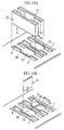
- Fig. 1 through Fig. 3 show an electronic component as an embodiment of the present invention.
- This electronic component X is made as a diode, and includes a first lead 1 having an island 10, and a second lead 2 having a connecting portion 20.
- the island 10 is mounted with a semiconductor chip 3.
- the semiconductor chip 3 has an upper surface electrode 30 electrically connected with the connecting portion 20 via a wire 4.
- the island 10, the connecting portion 20, the semiconductor chip 3 and the wire 4 are sealed by a resin package 5.
- Each of the leads 1, 2 has a portion extending out of the resin package 5.
- These extensions 11, 21 are respectively bent into crank-like shapes, so that their respective tips 11a, 21a are flush with a bottom surface of the resin package 5.
- the island 10 and the connecting portion 20 are opposed to each other, but their respective opposing side surfaces 10a, 20a are not in parallel to each other. More specifically, the side surface 10a of the island 10 is a flat surface, whereas the side surface 20a of the connecting portion 20 is a triangular, non-flat surface, i.e. like a two-fold surface including two flat surfaces. Therefore, the apex of the triangular side surface 20a represents the closest point to the side surface 10a of the island 10, and the distance between the side surfaces 10a, 20a grows larger toward respective outward ends.
- the island 10 and the connecting portion 20 are placed close to each other as a whole, thereby achieving the size reduction of the electronic component X, yet the distance between the side surface 10a, 20a increases toward the respective outward ends, enabling to reduce an amount of electric charge held between the side surfaces 10a, 20a.
- the gap between the side surface 10a, 20a is crossed by the wire 4 which serves as an electrical path, and is inherently prone to electric charging. Therefore, it is advantageous to provide such an arrangement in which the gap between the side surfaces 10a, 20a is not prone to electric charge.
- the electronic component X according to the present embodiment does not easily hold electric charge between the leads 1, 2, and therefore can be used appropriately even in a high frequency circuit.
- the electronic component X described above is manufactured from a leadframe 6 (See Fig. 3) obtained from an electrically conductive plate.
- the leadframe 6 is formed by first punching the first and the second lead 1, 2 as a mutually connected single piece (a left-hand portion in Fig. 3), using a metal die (not illustrated) of a predetermined punching pattern. Then, another metal die (blade) P is used to punch out a gap (a region enclosed by phantom lines in the left-hand portion in Fig. 3) between the leads 1, 2 (a right-hand portion in Fig. 3).
- the smallest distance between the side surface 20a of the connection portion 20 of the second lead 2 and the side surface 10a of the first lead 1 is small as ever, yet the distance between the side surfaces 10a, 20a as a whole is larger than the convention. Therefore, the thickness of the metal die P necessary for the formation of the leadframe 6, i.e. each of the leads 1, 2, can be increased except for a certain part, enabling to reduce fracture and chipping of the metal die, leading to an increased life of the metal die P and improved cost of manufacture.
- the side surface 20a of the connecting portion 20 of the second lead 2 is formed as a triangular, non-flat surface (a folded surface).
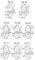
- the mutually opposed side surfaces 10a, 20a of the first lead 1 and the second lead 2 may be shaped as shown in Fig. 4 through Fig. 9, for achieving a non-parallel arrangement. Any of these arrangements provides the advantage same as described above.
- Fig. 4A shows a case in which the side surface 20a of the connecting portion 20 of the second lead 2 is formed like a convex arc (curved surface) .
- the side surface 10a of the die pad 10 of the first lead 1 may be formed as a triangular non-flat surface, or as shown in Fig. 4C, the side surface 10a may be formed like a convex arc to achieve a non-parallel arrangement between the side surfaces 10a, 20a.
- Fig. 5A and Fig. 5B show embodiments in which both of the mutually opposed side surfaces 10a, 20a of the first and the second leads 1, 2 are formed like the triangular, non-flat surfaces or like the convex arc surfaces, to achieve a non-parallel arrangement between the side surfaces 10a, 20a.
- one of the side surfaces 10a, 20a may be formed like the triangular, non-flat surface, whereas the other is formed like the convex arc surface, to achieve a non-parallel arrangement between the side surfaces 10a, 20a.
- Fig. 6 shows embodiments in which at least one of the side surfaces 10a, 20a is formed as a V-shaped, recessing and non-flat surface (a folded surface), to achieve a non-parallel arrangement between the side surfaces 10a, 20a.
- Fig. 6A shows a case in which the side surface 20a of the connecting portion 20 is formed into the V-shaped non-flat surface.
- Fig. 6B shows a case in which the side surface 10a of the island 10 is formed into the V-shaped non-flat surface
- Fig. 6C shows a case in which both of the side surfaces 10a, 20a are formed into the V-shaped non-flat surfaces.
- at least one of the side surfaces 10a, 20a may be formed like a concave, arced surface, to achieve a non-parallel arrangement between the side surfaces 10a, 20a.
- Fig. 7 shows embodiments in which at least one of the side surfaces 10a, 20a is formed as a slanted surface to achieve a non-parallel arrangement between the side surfaces 10a, 20a.
- Fig. 7A shows a case in which the side surface 20a of the connecting portion 20 is slanted with respect to the side surface 10a of the island 10.
- Fig. 7B shows a case in which the side surface 10a of the island 10 is slanted with respect to the side surface 20a of the connecting portion 20, and
- Fig. 7C shows a case in which both of the side surfaces 10a, 20a are slanted.
- Fig. 8 shows embodiments in which at least one of the side surfaces 10a, 20a is formed trapezoidal, i.e. with two widthwise sides being slanted and the intermediate portion being horizontal to achieve a non-parallel arrangement between the side surfaces 10a, 20a.
- Fig. 8A shows a case in which the side surface 20a of the connecting portion 20 is formed trapezoidal.
- Fig. 8B shows a case in which the side surface 10a of the island 10 is formed trapezoidal
- Fig. 8C shows a case in which both of the side surfaces 10a, 20a are formed trapezoidal.
- Fig. 9 shows embodiments in which at least one of the side surfaces 10a, 20a has its central portion projected as a stepped or a trapezoidal shape to achieve a non-parallel arrangement between the side surfaces 10a, 20a.
- Fig. 9A shows a case in which the side surface 20a of the connecting portion 20 is stepped.
- Fig. 9B shows a case in which the side surface 10a of the island 10 is stepped, and
- Fig. 9C shows a case in which both of the side surfaces 10a, 20a are stepped.
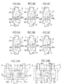
- Fig. 10 through Fig. 16 show embodiments in which the present invention is applied to electronic components having three to five terminals.
- Fig. 10 shows a principal portion of an electronic component including a first lead 1 having an island 10 and two second leads 2 each having a connecting portion 20.
- the island 10 is between the two connecting portions 20.
- Fig. 10A shows a case in which each connecting portion 20 has its side surface 20a facing respective one of the side surfaces 10a of the island 10 formed as a triangular, non-flat surface.
- Fig. 10B shows a case in which each of the respective side surfaces 10a of the island 10 facing a corresponding side surface 20a of the connecting portion is formed as a convex surface.
- Fig. 11 shows a principal portion of an electronic component including one second lead 2 having a connecting portion 20 and two first leads 1 each having an island 10.
- the connecting portion 20 is between the two islands 10.
- Fig. 11A shows a case in which each island 10 has its side surface 10a facing respective one of the side surfaces 20a of the connecting portion 20 formed as a triangular, non-flat surface.
- Fig. 11B shows a case in which each of the side surfaces 10a of the island 10 is formed as a convex surface.
- Fig. 10 and Fig. 11 cover cases in which the side surfaces 10a of the island 10 or the side surfaces 20a of the connecting portion(s) are formed as triangular, non-flat surfaces or convex surfaces.
- the side surfaces 10a, 20a of both elements may be made as folded or convex surfaces.
- the side surfaces 10a, 20a may be shaped as already described with reference to Fig. 6 through Fig. 9, i.e. the shape of V, concave, trapezoidal, stepped or even others.
- Fig. 12 shows embodiments, in each of which the present invention is applied to an electronic component having four terminals.
- Fig. 12A shows an embodiment in which the present invention is applied to an electronic component which includes one first lead 1 and three second leads 2.
- the three connecting portions 20 are disposed along two sides 5a, 5b which define a corner 50 of a resin package 5.
- the island 10 is placed to occupy a central region and a corner 51 which is diagonal with respect to the corner 50.
- the island 10 has two arced side surfaces 10a each facing a side surface 20a of one of the connecting portions 20.
- Fig. 12B shows an embodiment in which the present invention is applied to an electronic component including two first leads 1 and two second leads 2.
- the two connecting portions 20 of the respective second leads 2 are disposed along a side 5a of a resin package 5.
- the islands 10 of the respective first leads 1 are placed to occupy a central region and a side 5c which is a side facing away from the side 5a.
- each island 10 has an arced side surface 10a facing a side surface 20a of the corresponding connecting portion 20.
- one of the islands 10 has its side surface 10b arced.
- mutually facing side surfaces 10b of mutually adjacent islands 10 are also made non-parallel to each other.
- Fig. 12C shows an embodiment similar to the one shown in Fig. 12B, i.e. the present invention is applied to an electronic component including two first leads 1 and two second leads 2.
- the two islands 10 of the respective first leads 1 are disposed respectively at one of mutually diagonal corners 50, 51 of a resin package 5.
- the connecting portions 20 of the second leads 2 are placed respectively at the remaining corners 52, 53.
- an appropriate one of mutually facing side surfaces 10a, 20 of the mutually adjacent first and the second leads 1, 2 is arced or slanted so as to be non-parallel to each other.
- Fig. 12D shows an embodiment in which the present invention is applied to an electronic component including three first leads 1 and one second lead 2.
- each of the leads 1, 2 is disposed at one of the four corners 50-53 of a resin package 5.
- Appropriate ones of mutually facing side surfaces 10a, 10b, and 20a of the mutually adjacent leads 1, 2 are arced to achieve non-parallel arrangement between mutually facing side surfaces of the islands 10 and the connecting portions 20.
- the shape of mutually facing side surfaces 10a, 10b, 20a, 20b may be other than shown in Figs . 12A-12D so long as mutually facing leads 1, 2 are made non-parallel to each other.
- Fig. 13 through Fig. 16 show embodiments, in each of which the present invention is applied to an electronic component having five terminals.
- Fig. 13A-Fig. 13C show electronic components each having one island 10 at a central region of a resin package 5 and four connecting portions 20 around the island 10.
- either the island 10 or the connecting portions 20 have their respective appropriate side surfaces 10a, 20a arced, to achieve a non-parallel relationship of the side surfaces 10a of the island 10 with respect to opposing side surfaces 20a.
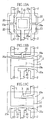
- Fig. 14A through Fig. 14F show embodiments, in each of which the present invention is applied to an electronic component having two first leads 1 and three second leads 2.
- Fig. 15A through Fig. 15E show embodiment, in each of which the present invention is applied to an electronic component having three first leads 1 and two second leads 2.
- Fig. 16A through Fig. 16C show embodiments, in each of which the present invention is applied to an electronic component having four first leads 1 and one second lead 2.
- mutually adjacent leads 1, 2 have their appropriate one(s) of side surfaces 10a, 10b, 20a, 20b arced or slanted.
- the shape of mutually facing side surfaces 10a, 10b, 20a, 20b may be other than shown in Figs. 13 through Fig. 16 so long as mutually facing leads 1, 2 are non-parallel to each other.
- the technical concept of the present invention is applicable also to an electronic component having six or more terminals, and even to electronic component having not more than five terminals which are not shown in Fig. 1 through Fig. 16.
Landscapes
- Lead Frames For Integrated Circuits (AREA)
Abstract
The present invention relates to an electronic component
formed of an electrically conductive plate and including a
plurality of leads 1, 2 each having an island 10 for mounting
of a semiconductor chip 3 or having a connecting portion 20
for connection with a wire 4. According to an electronic
component X offered by the present invention, at least a set
of mutually adjacent leads 1, 2 have their respective mutually
facing side surfaces 10a, 20a made non-parallel to each other.
Preferably, at least one side surface 20a (10a) of the leads
1, 2 is at least partially curved, folded and/or slanted.
Description
The present invention relates to an electronic component
made of an electrically conductive plate and including a
plurality of leads formed with an island for mounting of a
semiconductor chip or formed with a connecting portion for
connection with a wire. Such an electronic component serves
as e.g. a diode, a transistor, or a combination of these.
As an example of the electronic component, Fig. 17 and
Fig. 18 show a two-terminal electronic component Y, which
serves as a diode. The electronic component Y includes a
first lead 7 formed with an island 70, and a second lead 8
formed with a connecting portion 80. These leads 7, 8 are
opposed to each other so that their respective end surfaces
70a, 80a face in parallel to each other. The island 70 is
mounted with a semiconductor chip 9. The semiconductor chip
9 has an upper surface electrode 90 electrically connected
with the connecting portion 80 via a wire 91. With the above
structure, the semiconductor chip 9, the wire 91, the island
70 and the connecting portion 80 are entirely sealed in a resin
package 92. Each of the leads 7, 8 extends out of the resin
package 92. These extensions 71, 81 serve as outer connection
terminals. More specifically, as shown in Fig. 18, the
extensions 71, 81 are respectively bent into crank-like
shapes, so that their respective tips 71a, 81a are flush with
a bottom surface 92a of the resin package 92. Alternatively,
the extensions 71, 81 are bent as shown in phantom lines in
the figure. In each case, the tips 71a, 81a of the extensions
71, 81 serve as connecting portions with e.g. a circuit
substrate.
Now, with such a structure of the electronic component
Y, in view of miniaturizing the electronic component Y, it
is necessary to decrease the area of the island 70 and the
connecting portion 80. On the other hand, the size of the
semiconductor chip 9 mounted on the island 70 is largely
determined by the kind of electronic component Y to be
manufactured, which substantially limits the extent of area
reduction of the island 70. Likewise, the connecting portion
80 to which the wire 91 is connected has to allow for a certain
minimum area, which substantially limits the extent of area
reduction. As a result, in order to reduce the size of the
electronic component Y, it is necessary to decrease a distance
between the island 70 and the connecting portion 80, i.e. a
distance between the end surfaces 70a, 80a of the leads 7,
8.
However, according to the electronic component Y, the
leads 7, 8 are electrically connected with each other, and
their respective end surfaces 70a, 80a are faced in parallel
to each other. Thus, if the distance between the end surfaces
70a, 80a is decreased, the gap between these end surfaces 70a,
80a functions as a capacitor. Moreover, the smaller the
distance between the end surfaces 70a, 80a, the greater is
the electric charge held in the gap, leading to a problem that
the electronic component Y cannot be used in a high frequency
circuit.
There is another problem. Specifically, each of the
leads 7, 8 of the electronic component Y shown in Fig. 17 and
Fig. 18 is made from a leadframe. This leadframe is formed,
as shown in Fig. 19A for example, by first punching the first
and the second lead 7, 8 as a mutually connected single piece,
using a metal die P1 of a predetermined punching pattern.
Next, as shown in Fig. 19B, another metal die (blade) P2 is
used to punch out the gap between the leads 7, 8. Therefore,
in order to decrease the gap between the end surfaces 70a,
80a of the leads 7, 8, the blade P2 must have a decreased
thickness. However, if the distance between the leads 7, 8
is to be decreased, the blade P2 for forming the leadframe
becomes susceptible to fracture or chipping, reducing the
life of the blade P2 and resulting in disadvantage not only
in cost but also in manufacturing efficiency in that the blade
P2 must be replaced frequently.
The present invention is made under the above
circumstances, and it is therefore an object of the present
invention to provide an electronic component which can be made
advantageously not only in terms of manufacturing cost but
also in terms of manufacturing efficiency, and which is
miniaturized yet appropriate for use in a high frequency
circuit.
An electronic component provided by the present invention
is formed of an electrically conductive plate, includes a
plurality of leads each including an island for mounting of
a semiconductor chip or including a connecting portion for
connection with a wire, and is characterized in that at least
a set of mutually adjacent leads have their respective
mutually facing side surfaces made non-parallel to each
other.
According to this arrangement, the mutually facing side
surfaces of the above set of leads are non-parallel to each
other, which means the distance between the side surfaces is
larger at a certain location and smaller at a certain location.
Therefore, even if the leads are brought closer to each other
as a whole for the sake of size reduction of the electronic
component, the distance between the side surfaces is larger
for a certain length. Thus, it becomes possible to
accordingly reduce electrostatic capacity between the leads.
As a result, the electronic component according to the present
invention can be used appropriately even in a high frequency
circuit.
Further, even if each lead is formed by punching out an
electrically conductive plate, if there is a region having
the large distance between the mutually adjacent leads, then
the punch (blade) can be given a large thickness in a portion
corresponding to the region having the large distance. This
enables to reduce fracture and chipping of the blade, leading
to an increased life of the blade and improved cost of
manufacture.
In order to make a non-parallel arrangement between the
mutually facing side surfaces in the set of mutually adjacent
leads, at least one side surface of the set of leads can be
at least partially curved, folded and/or slanted. Further,
as anticipated from that the mutually facing side surfaces
may include a folded surface, the term "side surface" implies
that the side surface may include not only one surface but
also a plurality of continuous surfaces.
According to a preferred embodiment, one lead of the set
has the island and the other lead of the set has the connecting
portion. Further, the mutually facing side surfaces in the
set of leads may be crossed by a wire which bridges these leads .
The problem that the gap between mutually facing side
surfaces functions as a capacitor is not unique to an
electronic component including one lead having an island and
another lead having a connecting portion. Rather, the
problem is common to other electronic components having three
or more terminals in which there is a plurality of leads of
one or both kinds. In this type of electronic component, the
electric charge tends to accumulate between mutually adjacent
leads which are electrically connected together. Therefore,
the non-parallel arrangement should be provided between leads
where the island and the connecting portion are adjacent to
each other, or between leads which are connected with each
other via a wire, in order to avoid the above-described
problem more effectively.
The technical concept of the present invention is
applicable to a variety of electronic components having leads
made from a leadframe, and particularly applied suitably to
an electronic component serving as a diode, a transistor or
a combination of these.
According to a preferred embodiment, the set of leads
includes at least three leads, and the side surface of one
of the leads faces the respective side surfaces of the other
leads.
Hereinafter, preferred embodiments of the present
invention will be described specifically, with reference to
the drawings.
Fig. 1 through Fig. 3 show an electronic component as an
embodiment of the present invention. This electronic
component X is made as a diode, and includes a first lead 1
having an island 10, and a second lead 2 having a connecting
portion 20.
The island 10 is mounted with a semiconductor chip 3. The
semiconductor chip 3 has an upper surface electrode 30
electrically connected with the connecting portion 20 via a
wire 4. The island 10, the connecting portion 20, the
semiconductor chip 3 and the wire 4 are sealed by a resin
package 5.
Each of the leads 1, 2 has a portion extending out of the
resin package 5. These extensions 11, 21 are respectively
bent into crank-like shapes, so that their respective tips
11a, 21a are flush with a bottom surface of the resin package
5.
The island 10 and the connecting portion 20 are opposed
to each other, but their respective opposing side surfaces
10a, 20a are not in parallel to each other. More specifically,
the side surface 10a of the island 10 is a flat surface, whereas
the side surface 20a of the connecting portion 20 is a
triangular, non-flat surface, i.e. like a two-fold surface
including two flat surfaces. Therefore, the apex of the
triangular side surface 20a represents the closest point to
the side surface 10a of the island 10, and the distance between
the side surfaces 10a, 20a grows larger toward respective
outward ends.
According to the above arrangement, the island 10 and the
connecting portion 20 are placed close to each other as a whole,
thereby achieving the size reduction of the electronic
component X, yet the distance between the side surface 10a,
20a increases toward the respective outward ends, enabling
to reduce an amount of electric charge held between the side
surfaces 10a, 20a. In particular, the gap between the side
surface 10a, 20a is crossed by the wire 4 which serves as an
electrical path, and is inherently prone to electric charging.
Therefore, it is advantageous to provide such an arrangement
in which the gap between the side surfaces 10a, 20a is not
prone to electric charge. As has been described, the
electronic component X according to the present embodiment
does not easily hold electric charge between the leads 1, 2,
and therefore can be used appropriately even in a high
frequency circuit.
The electronic component X described above is
manufactured from a leadframe 6 (See Fig. 3) obtained from
an electrically conductive plate. The leadframe 6 is formed
by first punching the first and the second lead 1, 2 as a
mutually connected single piece (a left-hand portion in Fig.
3), using a metal die (not illustrated) of a predetermined
punching pattern. Then, another metal die (blade) P is used
to punch out a gap (a region enclosed by phantom lines in the
left-hand portion in Fig. 3) between the leads 1, 2 (a
right-hand portion in Fig. 3).
According to the leadframe 6 formed in such a way, the
smallest distance between the side surface 20a of the
connection portion 20 of the second lead 2 and the side surface
10a of the first lead 1 is small as ever, yet the distance
between the side surfaces 10a, 20a as a whole is larger than
the convention. Therefore, the thickness of the metal die
P necessary for the formation of the leadframe 6, i.e. each
of the leads 1, 2, can be increased except for a certain part,
enabling to reduce fracture and chipping of the metal die,
leading to an increased life of the metal die P and improved
cost of manufacture.
According to the present embodiment, the side surface 20a
of the connecting portion 20 of the second lead 2 is formed
as a triangular, non-flat surface (a folded surface).
Alternatively, the mutually opposed side surfaces 10a, 20a
of the first lead 1 and the second lead 2 may be shaped as
shown in Fig. 4 through Fig. 9, for achieving a non-parallel
arrangement. Any of these arrangements provides the
advantage same as described above.
Fig. 4A shows a case in which the side surface 20a of the
connecting portion 20 of the second lead 2 is formed like a
convex arc (curved surface) . Alternatively, as shown in Fig.
4B, the side surface 10a of the die pad 10 of the first lead
1 may be formed as a triangular non-flat surface, or as shown
in Fig. 4C, the side surface 10a may be formed like a convex
arc to achieve a non-parallel arrangement between the side
surfaces 10a, 20a.
Fig. 5A and Fig. 5B show embodiments in which both of the
mutually opposed side surfaces 10a, 20a of the first and the
second leads 1, 2 are formed like the triangular, non-flat
surfaces or like the convex arc surfaces, to achieve a
non-parallel arrangement between the side surfaces 10a, 20a.
Obviously, though not illustrated, one of the side surfaces
10a, 20a may be formed like the triangular, non-flat surface,
whereas the other is formed like the convex arc surface, to
achieve a non-parallel arrangement between the side surfaces
10a, 20a.
Fig. 6 shows embodiments in which at least one of the side
surfaces 10a, 20a is formed as a V-shaped, recessing and
non-flat surface (a folded surface), to achieve a non-parallel
arrangement between the side surfaces 10a, 20a.
Specifically, Fig. 6A shows a case in which the side surface
20a of the connecting portion 20 is formed into the V-shaped
non-flat surface. Fig. 6B shows a case in which the side
surface 10a of the island 10 is formed into the V-shaped
non-flat surface, and Fig. 6C shows a case in which both of
the side surfaces 10a, 20a are formed into the V-shaped
non-flat surfaces. Obviously, though not illustrated, at
least one of the side surfaces 10a, 20a may be formed like
a concave, arced surface, to achieve a non-parallel
arrangement between the side surfaces 10a, 20a.
Fig. 7 shows embodiments in which at least one of the side
surfaces 10a, 20a is formed as a slanted surface to achieve
a non-parallel arrangement between the side surfaces 10a, 20a.
Specifically, Fig. 7A shows a case in which the side surface
20a of the connecting portion 20 is slanted with respect to
the side surface 10a of the island 10. Fig. 7B shows a case
in which the side surface 10a of the island 10 is slanted with
respect to the side surface 20a of the connecting portion 20,
and Fig. 7C shows a case in which both of the side surfaces
10a, 20a are slanted.
Fig. 8 shows embodiments in which at least one of the side
surfaces 10a, 20a is formed trapezoidal, i.e. with two
widthwise sides being slanted and the intermediate portion
being horizontal to achieve a non-parallel arrangement
between the side surfaces 10a, 20a. Specifically, Fig. 8A
shows a case in which the side surface 20a of the connecting
portion 20 is formed trapezoidal. Fig. 8B shows a case in
which the side surface 10a of the island 10 is formed
trapezoidal, and Fig. 8C shows a case in which both of the
side surfaces 10a, 20a are formed trapezoidal.
Fig. 9 shows embodiments in which at least one of the side
surfaces 10a, 20a has its central portion projected as a
stepped or a trapezoidal shape to achieve a non-parallel
arrangement between the side surfaces 10a, 20a.
Specifically, Fig. 9A shows a case in which the side surface
20a of the connecting portion 20 is stepped. Fig. 9B shows
a case in which the side surface 10a of the island 10 is stepped,
and Fig. 9C shows a case in which both of the side surfaces
10a, 20a are stepped.
The embodiments described above are for electronic
components classified as two-terminal parts (such as a diode).
The technical concept of the present invention is also
applicable to electronic components having three or more
terminals. Hereinafter, Fig. 10 through Fig. 16 show
embodiments in which the present invention is applied to
electronic components having three to five terminals.
Fig. 10 shows a principal portion of an electronic
component including a first lead 1 having an island 10 and
two second leads 2 each having a connecting portion 20.
According to this electronic component, the island 10 is
between the two connecting portions 20. Specifically, Fig.
10A shows a case in which each connecting portion 20 has its
side surface 20a facing respective one of the side surfaces
10a of the island 10 formed as a triangular, non-flat surface.
On the other hand, Fig. 10B shows a case in which each of the
respective side surfaces 10a of the island 10 facing a
corresponding side surface 20a of the connecting portion is
formed as a convex surface.
Fig. 11 shows a principal portion of an electronic
component including one second lead 2 having a connecting
portion 20 and two first leads 1 each having an island 10.
According to this electronic component, the connecting
portion 20 is between the two islands 10. Specifically, Fig.
11A shows a case in which each island 10 has its side surface
10a facing respective one of the side surfaces 20a of the
connecting portion 20 formed as a triangular, non-flat
surface. On the other hand, Fig. 11B shows a case in which
each of the side surfaces 10a of the island 10 is formed as
a convex surface.
Fig. 10 and Fig. 11 cover cases in which the side surfaces
10a of the island 10 or the side surfaces 20a of the connecting
portion(s) are formed as triangular, non-flat surfaces or
convex surfaces. Alternatively, the side surfaces 10a, 20a
of both elements may be made as folded or convex surfaces.
Further, the side surfaces 10a, 20a may be shaped as already
described with reference to Fig. 6 through Fig. 9, i.e. the
shape of V, concave, trapezoidal, stepped or even others.
Fig. 12 shows embodiments, in each of which the present
invention is applied to an electronic component having four
terminals.
Fig. 12A shows an embodiment in which the present
invention is applied to an electronic component which
includes one first lead 1 and three second leads 2. According
to this electronic component, the three connecting portions
20 are disposed along two sides 5a, 5b which define a corner
50 of a resin package 5. The island 10 is placed to occupy
a central region and a corner 51 which is diagonal with respect
to the corner 50. In this layout, the island 10 has two arced
side surfaces 10a each facing a side surface 20a of one of
the connecting portions 20. Further, according to the
present invention, not only between the mutually facing side
surfaces 10a, 20a of the first and the second leads 1, 2, but
also between mutually facing side surfaces 20b of the second
leads 2, one of such side surfaces is arced or slanted to
achieve a non-parallel arrangement between the side surfaces
20b of the second leads 2.
Fig. 12B shows an embodiment in which the present
invention is applied to an electronic component including two
first leads 1 and two second leads 2. According to this
embodiment, the two connecting portions 20 of the respective
second leads 2 are disposed along a side 5a of a resin package
5. The islands 10 of the respective first leads 1 are placed
to occupy a central region and a side 5c which is a side facing
away from the side 5a. With this layout, each island 10 has
an arced side surface 10a facing a side surface 20a of the
corresponding connecting portion 20. Further, between the
mutually facing side surfaces 10b of the two islands 10, one
of the islands 10 has its side surface 10b arced. Thus,
according to the electronic component offered by the present
embodiment, mutually facing side surfaces 10b of mutually
adjacent islands 10 are also made non-parallel to each other.
Fig. 12C shows an embodiment similar to the one shown in
Fig. 12B, i.e. the present invention is applied to an
electronic component including two first leads 1 and two
second leads 2. In this embodiment, the two islands 10 of
the respective first leads 1 are disposed respectively at one
of mutually diagonal corners 50, 51 of a resin package 5. The
connecting portions 20 of the second leads 2 are placed
respectively at the remaining corners 52, 53. According to
this arrangement again, an appropriate one of mutually facing
side surfaces 10a, 20 of the mutually adjacent first and the
second leads 1, 2 is arced or slanted so as to be non-parallel
to each other.
Fig. 12D shows an embodiment in which the present
invention is applied to an electronic component including
three first leads 1 and one second lead 2. According to this
electronic component, each of the leads 1, 2 is disposed at
one of the four corners 50-53 of a resin package 5.
Appropriate ones of mutually facing side surfaces 10a, 10b,
and 20a of the mutually adjacent leads 1, 2 are arced to achieve
non-parallel arrangement between mutually facing side
surfaces of the islands 10 and the connecting portions 20.
Obviously, in the four-terminal electronic component,
too, the shape of mutually facing side surfaces 10a, 10b, 20a,
20b may be other than shown in Figs . 12A-12D so long as mutually
facing leads 1, 2 are made non-parallel to each other.
Fig. 13 through Fig. 16 show embodiments, in each of which
the present invention is applied to an electronic component
having five terminals.
Fig. 13A-Fig. 13C show electronic components each having
one island 10 at a central region of a resin package 5 and
four connecting portions 20 around the island 10. According
to these embodiments, either the island 10 or the connecting
portions 20 have their respective appropriate side surfaces
10a, 20a arced, to achieve a non-parallel relationship of the
side surfaces 10a of the island 10 with respect to opposing
side surfaces 20a.
Fig. 14A through Fig. 14F show embodiments, in each of
which the present invention is applied to an electronic
component having two first leads 1 and three second leads 2.
Fig. 15A through Fig. 15E show embodiment, in each of which
the present invention is applied to an electronic component
having three first leads 1 and two second leads 2. Fig. 16A
through Fig. 16C show embodiments, in each of which the
present invention is applied to an electronic component
having four first leads 1 and one second lead 2. In all of
these embodiments, mutually adjacent leads 1, 2 have their
appropriate one(s) of side surfaces 10a, 10b, 20a, 20b arced
or slanted.
Obviously, in the five-terminal electronic component,
too, the shape of mutually facing side surfaces 10a, 10b, 20a,
20b may be other than shown in Figs. 13 through Fig. 16 so
long as mutually facing leads 1, 2 are non-parallel to each
other.
Further, the technical concept of the present invention
is applicable also to an electronic component having six or
more terminals, and even to electronic component having not
more than five terminals which are not shown in Fig. 1 through
Fig. 16.
Claims (6)
- An electronic component formed of an electrically conductive plate, comprising a plurality of leads each including an island for mounting of a semiconductor chip or including a connecting portion for connection with a wire,
wherein at least a set of mutually adjacent leads have their respective mutually facing side surfaces made non-parallel to each other. - The electronic component according to Claim 1,
wherein at least one side surface of the set of leads is at least partially curved, folded and/or slanted. - The electronic component according to Claim 1,
wherein one lead of the set has the island and the other lead of the set has the connecting portion. - The electronic component according to Claim 1,
wherein the mutually facing side surfaces in the set of leads are crossed by a wire which bridges these leads. - The electronic component according to Claim 1,
serving as a diode, a transistor or a combination of these. - The electronic component according to Claim 1,
wherein the set of leads includes at least three leads, the side surface of one of the leads facing the respective side surfaces of the other leads.
Applications Claiming Priority (3)
| Application Number | Priority Date | Filing Date | Title |
|---|---|---|---|
| JP18853499 | 1999-07-02 | ||
| JP18853499 | 1999-07-02 | ||
| PCT/JP2000/004385 WO2001003184A1 (en) | 1999-07-02 | 2000-06-30 | Electronic part |
Publications (2)
| Publication Number | Publication Date |
|---|---|
| EP1207554A1 true EP1207554A1 (en) | 2002-05-22 |
| EP1207554A4 EP1207554A4 (en) | 2008-07-02 |
Family
ID=16225396
Family Applications (1)
| Application Number | Title | Priority Date | Filing Date |
|---|---|---|---|
| EP00942439A Withdrawn EP1207554A4 (en) | 1999-07-02 | 2000-06-30 | ELECTRONIC COMPONENT |
Country Status (5)
| Country | Link |
|---|---|
| US (1) | US6538306B1 (en) |
| EP (1) | EP1207554A4 (en) |
| KR (1) | KR100633113B1 (en) |
| CN (1) | CN1174487C (en) |
| WO (1) | WO2001003184A1 (en) |
Families Citing this family (12)
| Publication number | Priority date | Publication date | Assignee | Title |
|---|---|---|---|---|
| DE10142654A1 (en) * | 2001-08-31 | 2003-04-03 | Osram Opto Semiconductors Gmbh | Fuse component with visual display |
| JP4646480B2 (en) * | 2002-02-27 | 2011-03-09 | 三洋電機株式会社 | Semiconductor circuit storage device |
| JP2003258183A (en) * | 2002-03-04 | 2003-09-12 | Shinko Electric Ind Co Ltd | Lead frame manufacturing method |
| USD520466S1 (en) * | 2003-10-01 | 2006-05-09 | Kabushiki Kaisha Toshiba | Rectifier element diode |
| US20050148681A1 (en) * | 2003-10-02 | 2005-07-07 | Schoen Catherine A. | Photoinitiator and ink |
| JP3994095B2 (en) * | 2004-06-23 | 2007-10-17 | ローム株式会社 | Surface mount electronic components |
| USD562272S1 (en) * | 2006-11-17 | 2008-02-19 | Lighthouse Technology Co., Ltd. | Light emitting diode (LED) |
| US20190097524A1 (en) * | 2011-09-13 | 2019-03-28 | Fsp Technology Inc. | Circuit having snubber circuit in power supply device |
| JPWO2013047533A1 (en) * | 2011-09-29 | 2015-03-26 | シャープ株式会社 | Semiconductor device |
| TWI454195B (en) * | 2012-04-19 | 2014-09-21 | 中華映管股份有限公司 | Method for fixing semiconductor wafer on circuit substrate and structure thereof |
| US8633575B1 (en) * | 2012-05-24 | 2014-01-21 | Amkor Technology, Inc. | IC package with integrated electrostatic discharge protection |
| JP6630390B2 (en) * | 2018-03-29 | 2020-01-15 | アオイ電子株式会社 | Semiconductor device |
Family Cites Families (23)
| Publication number | Priority date | Publication date | Assignee | Title |
|---|---|---|---|---|
| US4794431A (en) * | 1986-04-21 | 1988-12-27 | International Rectifier Corporation | Package for photoactivated semiconductor device |
| JPS6343465A (en) | 1986-08-09 | 1988-02-24 | Fujitsu Ltd | Driving system for contact type image sensor |
| JP2524774Y2 (en) * | 1986-09-03 | 1997-02-05 | シャープ株式会社 | LED lamp |
| JPS63260155A (en) * | 1987-04-17 | 1988-10-27 | Hitachi Ltd | Semiconductor device |
| US4750675A (en) | 1987-10-05 | 1988-06-14 | General Motors Corporation | Damped opening poppet covered orifice fuel injection nozzle |
| JPH01278031A (en) * | 1988-04-28 | 1989-11-08 | Mitsubishi Electric Corp | Semiconductor device |
| JPH04137064A (en) | 1990-09-28 | 1992-05-12 | Canon Inc | Document processor |
| JPH04280664A (en) * | 1990-10-18 | 1992-10-06 | Texas Instr Inc <Ti> | Lead fram for semiconductor device |
| JP2519597Y2 (en) * | 1991-06-17 | 1996-12-04 | 日本電気株式会社 | Structure of semiconductor device |
| JPH0590643A (en) * | 1991-09-30 | 1993-04-09 | Victor Co Of Japan Ltd | Light emitting device |
| JPH05190751A (en) * | 1992-01-10 | 1993-07-30 | Nec Corp | Semiconductor device |
| DE4242842C2 (en) * | 1992-02-14 | 1999-11-04 | Sharp Kk | Light-emitting component for surface mounting and method for its production |
| JP2708320B2 (en) * | 1992-04-17 | 1998-02-04 | 三菱電機株式会社 | Multi-chip type semiconductor device and manufacturing method thereof |
| JPH05315493A (en) | 1992-05-08 | 1993-11-26 | Sony Corp | Lead frame for metal package use and semiconductor device manufactured using this |
| JPH0653554A (en) * | 1992-07-28 | 1994-02-25 | Rohm Co Ltd | Optical semiconductor device |
| JPH0685145A (en) * | 1992-09-02 | 1994-03-25 | Toshiba Corp | Semiconductor device |
| JP3117812B2 (en) | 1992-09-17 | 2000-12-18 | アピックヤマダ株式会社 | Lead frame and manufacturing method thereof |
| JPH06204569A (en) * | 1992-12-28 | 1994-07-22 | Casio Comput Co Ltd | Structure of light-emitting diode |
| JPH07307424A (en) | 1994-05-10 | 1995-11-21 | Hitachi Cable Ltd | Transistor lead frame |
| US5489800A (en) * | 1994-08-31 | 1996-02-06 | Motorola, Inc. | Dual channel small outline optocoupler package and method thereof |
| US5530284A (en) * | 1995-03-06 | 1996-06-25 | Motorola, Inc. | Semiconductor leadframe structure compatible with differing bond wire materials |
| US5739582A (en) * | 1995-11-24 | 1998-04-14 | Xerox Corporation | Method of packaging a high voltage device array in a multi-chip module |
| JPH09213855A (en) | 1996-01-30 | 1997-08-15 | Nec Corp | Lead frame for hollow plastic packages |
-
2000
- 2000-06-30 US US10/019,391 patent/US6538306B1/en not_active Expired - Lifetime
- 2000-06-30 KR KR1020017016916A patent/KR100633113B1/en not_active Expired - Fee Related
- 2000-06-30 WO PCT/JP2000/004385 patent/WO2001003184A1/en not_active Ceased
- 2000-06-30 EP EP00942439A patent/EP1207554A4/en not_active Withdrawn
- 2000-06-30 CN CNB008096589A patent/CN1174487C/en not_active Expired - Lifetime
Also Published As
| Publication number | Publication date |
|---|---|
| WO2001003184A1 (en) | 2001-01-11 |
| EP1207554A4 (en) | 2008-07-02 |
| KR100633113B1 (en) | 2006-10-11 |
| KR20020036968A (en) | 2002-05-17 |
| CN1174487C (en) | 2004-11-03 |
| US6538306B1 (en) | 2003-03-25 |
| CN1359537A (en) | 2002-07-17 |
Similar Documents
| Publication | Publication Date | Title |
|---|---|---|
| US10886204B2 (en) | Semiconductor device with lead terminals having portions thereof extending obliquely | |
| US5347429A (en) | Plastic-molded-type semiconductor device | |
| US6538306B1 (en) | Electronic part | |
| US20050035445A1 (en) | Power semiconductor module with deflection-resistant base plate | |
| JPH09260180A (en) | Low inductance capacitor | |
| JPH03177055A (en) | Substrate for mounting semiconductor element | |
| CN115050719A (en) | Semiconductor device with a plurality of semiconductor chips | |
| JPH07147359A (en) | Surface mount semiconductor device | |
| CN221687531U (en) | Power module packaging structure | |
| JP3372065B2 (en) | Surface acoustic wave device | |
| CN223566623U (en) | Packaging frame for matched use of double-switch device | |
| JPWO2001003184A1 (en) | Electronic Components | |
| EP1675179A1 (en) | Stacked-type semiconductor device | |
| US6118173A (en) | Lead frame and a semiconductor device | |
| KR100377267B1 (en) | Leadframe of die pad and method for manufacturing the same | |
| JP2758322B2 (en) | Circuit board for mounting electronic components | |
| JP2023179984A (en) | Lead frames and electronic components | |
| JPH0727187Y2 (en) | IC module for IC card | |
| WO2024134946A1 (en) | Power storage pack, semiconductor device, and method for manufacturing semiconductor device | |
| JP2000124365A (en) | Manufacture of module with integrated circuit chip used for ic card | |
| JPS62109330A (en) | Semiconductor device | |
| JPH04127679U (en) | circuit board | |
| JPH0714657U (en) | Semiconductor device | |
| JPH0221644A (en) | Integrated circuit package | |
| JPH08162310A (en) | Chip resistor network |
Legal Events
| Date | Code | Title | Description |
|---|---|---|---|
| PUAI | Public reference made under article 153(3) epc to a published international application that has entered the european phase |
Free format text: ORIGINAL CODE: 0009012 |
|
| 17P | Request for examination filed |
Effective date: 20020131 |
|
| RBV | Designated contracting states (corrected) |
Designated state(s): DE FR IT NL |
|
| A4 | Supplementary search report drawn up and despatched |
Effective date: 20080603 |
|
| RIC1 | Information provided on ipc code assigned before grant |
Ipc: H01L 23/495 20060101AFI20080528BHEP |
|
| 17Q | First examination report despatched |
Effective date: 20081223 |
|
| STAA | Information on the status of an ep patent application or granted ep patent |
Free format text: STATUS: THE APPLICATION IS DEEMED TO BE WITHDRAWN |
|
| 18D | Application deemed to be withdrawn |
Effective date: 20090505 |