TECHNICAL FIELD
This invention relates to a display device. The invention is
especially effective for the reflective liquid-crystal display (LCD) or
organic EL display (OELD), which is intended to achieve space saving while
reducing electric power.
BACKGROUND OF THE INVENTION
Recently, the display devices using liquid crystal (hereinafter,
referred to as display) is spreading at conspicuous pace. The display of
this type is low in power consumption and improved in saving space, in
comparison with a CRT display. Accordingly, it is important to make use of
the merits of such a display and produce a display that is lower in power
consumption and improved in saving space.
Fig. 15 is a block diagram of a system for providing display on a
display device by a TFT display. This system is configured with a digital
interface 100 and a TFT liquid crystal display panel 101. The digital
interface 100 is configured, at least, with a CPU 100A, a RAM 100B, a frame
memory 100C and an LCD controller 100D. The CPU 100A is operation control
means for transmitting display data while exchanging data with the RAM 100B
as a general-purpose memory. Because this RAM 100B is not especially used
merely as a memory for display, there is newly a need of a memory for
storing the data for display. That is the frame memory 100C. The frame
memory 100C temporarily stores the display data in an amount of one screen
of the liquid crystal panel 101C (hereinafter, the data in an amount of one
pixel is referred to as display data, and each binary signal constituting
the display data is referred to as an image signal). The LCD
controller 100D carries out transmission control of display data in order to
display, in timing, each of display data stored in the frame memory 100C in a
display position on the liquid crystal panel 101C. Herein, for a CRT there is
a necessity to transmit display data through conversion into analog data. It
is however considered that the interface of the liquid crystal display is
compatible with digital data, and herein the display data is transmitted by an
image signal as digital data.
Meanwhile, the TFT liquid crystal display panel 101 is configured with
a scanning line driver 101A, a digital data driver 101B and a liquid crystal
panel 101C. The scanning line driver 101A carries out display control in a
scanning line (row) direction on the basis of the timing data transmitted from
the LCD controller 100D. The digital data driver 101B is allowed to receive
and process the digital-data image signal. The digital data driver 101B carries
out display control in a data-line (column) direction on the basis of the timing
data transmitted from the LCD controller 100D. On that occasion, it also controls
the tonal levels of display. The liquid crystal panel 101C is a panel having
TFTs (Thin Film Transistors) to effect display under the control of the scanning
line driver 101A and digital data driver 101B.
Such a system requires a frame memory 100C for temporarily store the
display data in an amount of all over the screen. Furthermore, an LCD controller
100D is required to transmit an image signal for the display data to the digital
data driver 101B.
Consequently, the system overall requires many of means thus increasing
its scale. Moreover, the reduction of consumed power cannot be achieved because
of a great deal of the amount of transmitting such data and large power
consumption as a result thereof.
Therefore, it is a problem of the present invention to provide a display
device capable of achieving space saving and consumed power reduction for the
system overall.
DISCLOSURE OF THE INVENTION
In order to solve the problem as above, a display device according to
the present application comprises: a storing section for storing a digital data
signal for controlling display; and a display control section for performing
display control on the basis of the digital data signal stored by the storing
section; provided in each dot as a minimum unit of display and arranged on a
semiconductor or insulating substrate.
BRIEF DESCRIPTION OF THE DRAWINGS
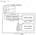
Fig. 1 is a block diagram representing a concept of a system including
a display device according to a first embodiment of the present invention.
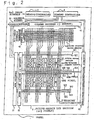
Fig. 2 is a diagram representing in detail a drive section of a panel
1.
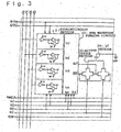
Fig. 3 is a diagram representing an equivalent circuit configured in each
dot of an active-matrix LCD section 2.
Fig. 4 is a diagram representing a relational example of drive waveforms
of VLC and VCOM.
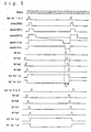
Fig. 5 is a diagram representing each drive waveform example of the
signals inputted by a row driver 3 and the digital data driver 4.
Fig. 6 is a diagram representing in detail a drive section of the panel
1A according to a second embodiment of the invention.
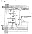
Fig. 7 is a diagram representing an equivalent circuit configured in each
dot of an active-matrix OELD section 2A.
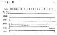
Fig. 8 represents a one-period waveform of PWMCLK in a third embodiment.
Fig. 9 is a diagram representing in detail a drive section of a panel
1B according to a fourth embodiment of the invention.
Fig. 10 is a diagram representing an equivalent circuit configured in
each dot of an active-matrix OELD section 2B.
Fig. 11 is a diagram representing in detail a drive section of a panel
1C according to a fifth embodiment of the invention.
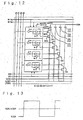
Fig. 12 is a diagram representing an equivalent circuit configured in
each dot of an active-matrix LCD section 2C.
Fig. 13 represents a waveform of an alternating current signal VLCON in
a fifth embodiment.
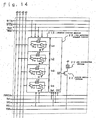
Fig. 14 is a diagram representing an equivalent circuit configured in
each dot in a sixth embodiment of the invention.
Fig. 15 is a block diagram of a system for performing display by a display
device due to a TFT display.
(Explanation of reference numerals)
1, 1A, 1B, 1C Panel
2, 2C Active-matrix LCD section
2A, 2B Active-matrix OELD section
21, 21A, 21B Storing circuit section
22, 22A, 22B, 22C Active device section
23 PWM waveform forming circuit
24, 24A, LC section
25, 25A, OEL luminescent section
3 Row driver section
31, 31A Row decoder
32 Word line driver
4 Digital data driver section
41 Column decoder
42 Input control circuit
43, 43A, 43B Column selection switch section
5 Memory controller
6, 6A Timing controller
61 Address buffer
62, 62A, PWM timing signal generating circuit
110 Digital interface
110A CPU
DETAILED DESCRIPTION OF THE INVENTION
A display device comprises: a storing section for storing a digital data
signal for controlling display; and a display control section for performing
display control on the basis of the digital data signal stored by the storing
section; provided in each dot as a minimum unit of display and arranged on a
semiconductor or insulating substrate.
In this display device, in order to control on-screen display, the storing
section for storing a signal and the display control section for controlling
on-screen display on the basis of the signal stored by the storing section are
provided in each dot. Furthermore, they are integrated on a semiconductor or
insulating substrate, i.e. within each dot array pattern. Power reduction is
achieved by the space saving due to the decrease of the circuits to be structured
in an area other than the display region and storing all the signals required
for on-screen display.
Also, a display device according to the invention comprises: a storing
section configured by one or a plurality of storing circuits provided at each
of interconnections of a plurality of write lines and a plurality of data lines
correspondingly to an array pattern of a dot as a minimum unit of display so
that, when a write signal is transmitted through the write line and an. image
signal as a digital data signal for controlling display is transmitted through
the data line, the image signal is stored; a converting section for converting
a value based on a value of the image signal stored by the storing section into
an analog signal; and a display control section for performing tonal control
using a liquid crystal on the basis of an analog signal converted by the
converting section; provided in each dot as a minimum unit of display and arranged
on a semiconductor or insulating substrate.
In this display device, the storing section configured by one or a
plurality of storing circuits is provided at each intersection of a plurality
of write lines and a plurality of data lines, to store in the storing section
all the image signals required for on-screen display. The converting section
converts the value based on the image signals into an analog signal on a
dot-by-dot basis, and the display control section performs tonal control using
a liquid crystal on the basis of the analog signal. These are integrated on
a semiconductor or insulating substrate, i.e. within each dot array pattern.
Also, in a display device according to the invention, the storing circuit
of the storing section is configured by a static circuit.
In this display device, the storing circuit is configured by a static
circuit thereby achieving to hold the image signals in a term as long as possible.
Also, the converting section of the display device according to the
invention pulse-width-modulates the value based on the image signal to convert
the same into the analog signal.
In this display device, the converting section performs pulse width
modulation in converting the value based on the image signals into an analog
signal.
Also, the converting section of the display device according to the
invention converts the value based on the image signal into the analog signal
modulated to a pulse width based on a γ-characteristic.
In this display device, the converting section performs pulse width
modulation based on a γ-characteristic in converting the value based on the image
signals into an analog signal.
Also, the converting section of the display device according to the
invention performs conversion into the analog signal at a constant period
interval.
In this display device, a constant period is provided as a unit because
control is made by converting the value based on the image signals into a time
based on a pulse width. Also, where display control is made, for example, with
a liquid crystal, there is a need to perform refresh at a constant time interval.
For this reason, it is more convenient to perform conversion at a constant time
interval
Also, in the converting section of a display device according to the
invention, provided is a duration that no conversion into an analog signal is
made in a duration of a constant period.
In this display device, a duration that no conversion into the analog
signal is made is provided in a duration of the constant period. In this duration,
the image signals are changed to the storing section.
Also, in the converting section of a display device according to the
invention, a start time of the constant period is different between the
converting sections, and the period no conversion into the analog signal is made
is different.
In this display device, in order to suppress flicker, a start time of
the constant period is different between the converting sections, and the
duration no conversion into an analog signal is made is different. Actually,
this is made for each converting section on a row-unit or column-unit basis from
a relationship of control, etc.
Also, an alternating current drive voltage is applied to the display
control section of a display device according to the invention.
In this display device, where display control is made using a liquid
crystal, voltage application if deviated shorten the lifetime from the viewpoint
of characteristics of a liquid crystal. Accordingly, an alternating current
drive voltage is applied.
Also, in a display device according to the invention, the alternating
current drive voltage is a voltage driven at VCOM±Va with respect to a reference
voltage VCOM.
In this display device, in order to suppress power consumption, the
alternating current drive voltage is given a voltage driven at VCOM±Va so as
to vary only the alternating current drive voltage on the basis of a reference
voltage.
Also, in a display device according to the invention, the alternating
current drive voltage is a voltage alternating-current-inversion-driven by two
voltage-applying lines laid correspondingly to the dot array pattern.
In this display device, in order to simplify the circuit configuration,
the alternating current drive voltage is such a voltage as
alternating-current-inversion-driven by two voltage-applying lines laid
correspondingly to the dot array pattern.
Also, a display device according to the invention, a plurality of rows
of the dot array are provided by groups, and rows in pair are set in each of
the groups to invert a phase of the alternating current drive voltage applied.
In this display device, in order to suppress flicker, rows in pair are
set in each of the groups to invert a phase of the alternating current drive
voltage applied.
Also, the display control section of a display device according to the
invention controls light emission of current-driven luminescent devices in
connection on the basis of the analog signal in place of performing tonal control
using a liquid crystal, thereby effecting tonal control.
In this display device, the display control section is connected with
current-driven luminescent devices spontaneously emitting light by current
drive so that emitted light is controlled on the basis of the analog signal
thereby achieving tonal control.
Also, a display device according to the invention comprises: a storing
section configured by one or a plurality of storing circuits provided at each
of interconnections of a plurality of write lines and a plurality of data lines
correspondingly to an array pattern of a dot as a minimum unit of display so
that, when a write signal is transmitted through the write line and an image
signal as a digital data signal for controlling display is transmitted through
the data line, the image signal is stored; one or a plurality of active devices
provided respectively connected to the storing circuits of the storing section
and current-driven luminescent devices having areas corresponding to place
values represented by image signals stored in the storing circuits, a display
control section provided in each dot to control emission of light of the
current-driven luminescent devices on the basis of the values of the image
signals stored in the storing circuits, and these are arranged on a semiconductor
or insulating substrate.
In this display device, a storing section configured by one or a plurality
of storing circuits is provided at each of interconnections laid with a plurality
of write lines and a plurality of data lines, to store all the image signals
required for on-screen display in each storing section. In the diaplay control
section, one or a plurality of active devices provided respectively connected
to the storing circuits of the storing section and current-driven luminescent
devices having areas corresponding to place values represented by image signals
stored in the storing circuits controls the current to be supplied to the
current-driven luminescent devices on the basis of a value of the image signals
(e.g. 0 or 1), thereby controlling light emission. These are integrated on a
semiconductor or insulating substrate, i.e. within each dot array pattern.
Also, a display device according to the invention has said current-driven
luminescent devices structured by EL devices.
In this display device, display is made by the EL devices as one kind
of a current-drive luminescent device having the features of reduced thickness,
high definition, reduced power consumption, etc.
Also, a display device according to the invention has the current-driven
luminescent devices structured by organic EL devices.
In this display device, display is made by an organic EL devices having
the further features of inexpensive, low-temperature process and so on, besides
the features of reduced thickness, high definition, reduced power consumption,
etc. possessed by the EL devices.
Also, a display device according to the invention comprises: a storing
section configured by one or a plurality of storing circuits provided at each
of interconnections of a plurality of write lines and a plurality of data lines
correspondingly to an array pattern of a dot as a minimum unit of display so
that, when a write signal is transmitted through the write line and an image
signal as a digital data signal for controlling display is transmitted through
the data line, the image signal is stored; one or a plurality of active devices
provided respectively connected to the storing circuits of the storing section
and liquid crystal driving sections having areas corresponding to place values
represented by image signals stored in the storing circuits, a display control
section provided in each dot to perform drive control using a liquid crystal
on the basis of the values of the image signals stored in the storing circuits,
and these are arranged on a semiconductor or insulating substrate.
In this display device, a storing section configured by one or a plurality
of storing circuits is provided at each of the each of interconnections laid
with a plurality of write lines and a plurality of data lines, to store all the
image signals required for on-screen display in each storing section. In the
display control section, one or a plurality of active devices provided
respectively connected to the storing circuits of the storing section and liquid
crystal drive sections, e.g. pixel electrodes, having areas corresponding to
place values represented by image signals stored in the storing circuits controls
the current to be supplied to the liquid crystal drive sections on the basis
of a value of the image signals (e.g. 0 or 1), thereby controlling the brightness
of display due to the liquid crystal. These are integrated on a semiconductor
or insulating substrate, i.e. within each dot array pattern.
Also, a display device according to the invention further lays a plurality
of read lines correspondingly to the dot array pattern so that, if a read signal
is transmitted, the image signals stored in the storing circuits are read out
of the storing section.
In this display device, a plurality of read lines are laid correspondingly
to the dot array pattern so that, if a read signal is transmitted, the image
signals stored in the storing circuits are read out of the storing section thereby
effecting data inputting and outputting in the display device.
Also, a display device according to the invention comprises: a display
drive section having a plurality of word lines, a plurality of write lines and
a plurality, of data lines laid correspondingly to an array pattern of a dot as
a minimum unit of display, and a display control section operating, when at least
a write signal is transmitted through the write lines and the image signals are
transmitted through the data lines, on the basis of the storing section for
storing the image signals, the image signals and a word signal transmitted
through the word lines, provided in each of the dot array patterns; a word line
driver section for controlling transmission of a word signal to the word lines;
a row decoder section for selecting a row for transmitting a write signal to
the write lines, to transmit the write signal to a selected row; a column decoder
for selecting the data line; a column selection switch section for transmitting
the image signals as data signals for controlling display to the data line
selected by the column decoder section; integrated and integrally formed on a
semiconductor or insulating substrate.
In this display device, a display drive section is laid with a plurality
of word lines, a plurality of write lines and a plurality of data lines, and
a display control section operating on the basis of the storing section for
storing the image signals, the image signals and a word signal transmitted
through the word lines, that are provided in each of the dot array patterns.
Further, provided are a word line driver section for controlling transmission
of a word signal to the word lines, a row decoder section for selecting a row
for transmitting a write signal to the word lines to transmit the write signal
to a selected row, a column decoder for selecting the data line, a column
selection switch section for transmitting the image signals as data signals for
controlling display to the data line selected by the column decoder section.
These are integrated and integrally formed on a semiconductor or insulating
substrate.
Also, in the display drive section of a display device according to the
invention, a converting section for converting a value based on the image signals
stored in the storing section into an analog signal is provided in each dot array
pattern, and the display control section operates on the basis of the analog
signal and the word signal.
In this display device, in the display drive section, the converting
section is further provided between the storing section and the display control
section. Because the display control section operates on the basis of the image
signals, an analog signal, e.g. due to pulse modulation, is generated.
Also, in a display device according to the invention, said word lines
are laid to transmit the word signal to the display control section on two rows.
In this display device, in order to reduce interconnections, the word
lines as power supply lines are shared between the display control sections,
for example, on the upper and lower two rows, to transmit a word signal (supply
power).
Also, the word line driver section and the row decoder section in a display
device according to the invention are allocated correspondingly to a length of
the display drive section in a row direction, and the column decoder section
and the column selection switch section are allocated correspondingly to a length
of the display drive section in a column direction.
In this display device, in order to size-reduce the layout in an area
other than display, the word line driver section and the row decoder section
are allocated correspondingly to a length of the display drive section in a column
direction, and the row decoder section and the column selection switch section
are allocated correspondingly to a length of the display drive section in a column
direction, thereby achieving space saving.
Also, each column selection switch structuring the column selection
switch of a display device according to the invention is allocated
correspondingly to a width of the dot array pattern.
In this display device, each column selection switch is allocated
corresponding to the width of the dot array pattern, in order to provide efficient
layout.
Also, a display device according to the invention, said row decoder
section selects a row for transmitting the write signal on the basis of an address
signal representing a storage position.
In this display device, in order to enable selection of an arbitrary row,
the row decoder section selects a row for transmitting the write signal on the
basis of an address signal.
Also, the column decoder section of a display device according to the
invention selects the data lines on the basis of the address signal.
In this display device, in order to enable an arbitrary data line
(column), the column decoder section transmits a data line on the basis of an
address signal.
Also, in a display device according to the invention, three dots for
developing and displaying in red, blue and green as light source colors are
provided as one pixel, the image signals are inputted on a one-pixel-unit basis,
and the column decoder section selects data lines for storing the image signals
in an amount of one pixel.
In this display device, in color display, three dots for developing and
displaying in red, blue and green as light source colors are provided as one
pixel. The image signals are inputted on a one-pixel-unit basis as a reference
of change of display. Also, the column decoder section selects data lines for
storing the image signals in an amount of one pixel.
Also, in the display device according to the invention, that three dots
for developing and displaying in red, blue and green as light source colors are
provided as one pixel, the image signals are inputted on a one-pixel-unit basis,
and the column decoder section selects data lines for storing the image signals
in an amount of a plurality of pixels.
In this display device, in the case of performing color display, in order
to reduce the clock frequency for use in storage, the image signals are inputted
on a plurality-of-pixels-unit basis. The column decoder section selects data
lines in an amount of a plurality of pixels.
Also, a display device according to the invention further comprises: a
timing controller section for controlling at least timing of transmitting the
address signal; a memory controller section for controlling transmission of the
image signals; further integrated and integrally formed on the substrate.
In this display device, the peripheral circuits required for controlling
display are all systematically integrally formed on the same substrate.
Embodiments of the Invention
Next, preferred embodiments of the present invention will be explained
based on the drawings.
Embodiment 1
Fig. 1 is a block diagram representing a concept of a system including
a display device according to Embodiment 1 of the invention. Fig. 1 represents
a concept called a system-on-panel (SOP). SOP is a concept for integrally forming
all the circuit systems concerned with display, such as an active matrix,
peripheral drive circuit, memories and controllers, on an insulating substrate,
such as glass by the use of polycrystalline silicon TFTs or the like. For this
reason, it is possible to directly couple a panel to a CPU and hence to achieve
cost reduction, reliability improvement and space saving.
In Fig. 1, a digital interface 110 is configured with a CPU 110A to
transmit display data. Meanwhile, a panel 1 as a display device has a drive
section configured by an active-matrix LCD section 2, a row driver 3, a digital
data driver 4, a memory controller 5 and a timing controller 6.
Fig. 2 is a diagram showing in detail a drive section of the panel 1.
The active-matrix LCD section 2 uses active devices, such as TFTs and diodes,
to effect display and stores pixel signals in one screen by the use of a storage
circuit section. The active-matrix LCD section 2 is arrayed with pixels in the
number of i × j. The present invention, assumed on a color display, has
light-source colors of R (red), G (green) and B (blue) three dots (called also
as sub-pixels) of which configure one pixel. It is assumed herein that one dot
represent one point, as a minimum unit, for effecting display. For a
monochromatic display, one pixel equals to one dot.
Fig. 3 is a diagram representing an equivalent circuit configured in each
dot of the active-matrix LCD section 2. Each dot area includes data lines, word
lines, active devices arranged at the intersections of them (e.g. switch devices
by transistors, diodes or the like), DAC (e.g. a PWM waveform forming circuit)
and storage circuits (e.g. latch circuits). In the figure, 21 is a storage
circuit section (storage section) configured by one or a plurality of memory
cells (storage circuits). In the figure, four memory cells are provided. It
is herein assumed that each memory cell be static. Consequently, data can be
held without refresh at a constant time interval. Each memory cell, when inputted
with a Write signal, holds (stores) a binary signal (data) transmitted through
d0, d1, d2 or d3. Herein, because four memory cells are used for one dot, an
information amount of 4 bits (value in 16 combinations) can be held. Each dot
can represent a brightness (tonal level) based on that value. The number of
the memory cells is in the same as the number of a value k, hereinafter referred.
23 is a PWM waveform forming circuit (converting section). The PWM
waveform forming circuit 23 is a kind of a counter. This is so-called a
digital/analog converter (DAC) for representing as a PWM waveform (analog data
with a pulse width) a value represented by image signals on the basis of the
image signals (digital data) held by the storage circuit section 21. In order
to respond to an effective value of an applied voltage, for tonal representation
the LCD is required to convert a data signal into an analog signal. Furthermore,
in order to secure a lifetime of liquid crystal, there is the need to apply an
alternating voltage inverting at a constant time interval. For this reason,
the present embodiment first converts digital data once into a
time-base-modulated analog timing signal by the use of the PWM waveform forming
circuit 23, and thereafter applies an alternating current drive voltage VLC to
the liquid crystal by the use of that timing signal.
22 is an active device section (display control section), for example,
of TFTS (thin film transistors). The conventional active device has connections
between the drain (or source) and the data line and between the gate and the
word line. In Fig. 3, the configuration is by dynamic devices. Meanwhile, the
drain (or source) and the word line are in connection while the gate and the
data line are in connection. Consequently, the active devices in the present
embodiment do not switch by drive to the word lines but switches on the basis
of values based on image signals (pulse width due to PWM) to adjust the charge
(current to be supplied to the pixel electrodes) stored on the pixel electrodes
(not shown). The pixel electrode forms a capacitance with a counter electrode
through a liquid crystal (LC section 24). By a voltage applied between the pixel
electrode and the counter electrode, the optical rotatory power due to
liquid-crystal molecules is controlled to effect display control of the dots.
Moreover, even if the switch of the active device section 22 is off (non-operation
period), the pixel electrode is allowed to maintain its display state owing to
built-up charge until refreshing in the next time (until rewriting-display
data). 24 is an LC section. The LC section 24 is a to-be-driven part
actually not formed on the glass substrate. From the foregoing, storage
drive control on each dot is implemented by signal transmission (current
supply, voltage application) through the data lines (dl, d2, d3 and d4) and
the word lines (Write). Also, display drive control is implemented by
signal transmission through the word lines (VLC and VCOM), PWMCLK and Set.
Herein, VDD and VSS are provided to supply power to the storage circuit
section 21 and PWM waveform forming circuit 23. Meanwhile, the signal
lines of VDD, VSS, VLC, VCOM, PWMCLK and Set can be shared between two
rows. This achieves layout simplification due to the reduction of
interconnect lines, space saving, area increase of dot array patterns
(opening-ratio increase).
In Fig. 2, it is a row driver 3 to control the drive to the word
lines. The row driver 3 is structured by a row decoder 31 and a word line
driver 32. The row decoder 31 selects and transmits a Write signal to a
row of pixels for storing or rewriting (hereinafter, merely referred to as
"store") display data on the basis of input address data.
Fig. 4 is a diagram showing a relational example of VLC and VCOM
drive waveforms. The word line driver 32 drives the VLC and VCOM. Because
the LCD requires alternating drive, at least the VLC must be made in the
form of an alternating current. Fig. 4(a) is a waveform when VLC = VCOM ±
Va is given. Where the relationship between VLC and VCOM is given as in
Fig. 4(a), consumption current can be reduced because VCOM is
satisfactorily constant. Due to this, as the smaller the display area (the
number of pixels), the greater the power reduction can be achieved. This
accordingly is suited for a reflective LCD used for displaying characters
(letters, symbols, etc.). Also, because VCOM to be supplied commonly to
all the rows is constant regardless of time, each VLC can
be driven (scanned) with phase deviation. It is noted that, in this case, there
is increase in the number of power sources and complication in circuit
configuration.
On the other hand, Fig. 4(b) is a waveform when driving is made such that
VLC and VCOM are alternating-current inversion with opposite phase. In this
case, it is possible to reduce the number of power sources and simplify the
circuit structure. However, because VCOM itself changes in potential without
causing display, power is consumed by the capacitance between the
interconnections and the VCOM. Accordingly, there is increase in consumption
power by VCOM regardless of display area broadness. Meanwhile, VCOM is common
to all the rows as mentioned before. Accordingly, because all of the VLC must
be driven on the basis of the phase of VCOM, each of VLC cannot be driven (scanned)
with phase deviation.
On the other hand, it is a digital data driver 4 that drives the data
lines. The digital data driver 4 is configured with a column decoder 41, an
input control circuit 42 and a column selection switch section 43. The column
decoder 41 selects a column having the pixels to be stored (rewritten) with
display data from among the columns (in the number of j) on one row (line) on
the basis of input address data. This selects data lines to be driven. The
input control circuit 42 is a circuit for controlling one pixel of image signals
(k × 3) parallel-transmitted from the memory controller 5. As described before,
the value of k and the number of memory cells in the storage circuit section
21 are the same, which is the number required to represent the dots at a brightness
with tonal levels of 2k. Consequently, k = 4 is given in Fig. 2, wherein 16
tonal levels of brightness are to be set on each dot. The column selection switch
section 43 is provided correspondingly to the number of pixels (that is, k ×
3 × j) on one line on the basis of image signals (k × 3) per pixel as a unit.
Each column selection switch switches on the basis of the selection by the column
decoder 41 and image signals to transmit image signals onto (drive) the data
lines. The column selection switch is configured for arrangement
correspondingly to a width nearly the same as a width of the dot. Accordingly,
the column selection switch section 43 will not be longer in width than the active
matrix LCD section 2, and can be ideally laid out in view of interconnections.
The memory controller 5 controls as image signals of k × 3 the display
data transmitted from the CPU 110A. Also, the timing controller 6 has at least
an address buffer 61 and a PWM timing signal generating circuit 62, to transmit
an address signal to the row decoder 31 and column decoder 41 in order to store
the display data transmitted from the CPU 110A. Also, transmitted is a timing
signal for generating PWMCLK to the PWM timing signal generating circuit 62.
The PWM timing signal generating circuit 62 generates a PWMCLK as a reference
for forming a PWM waveform in the PWM waveform forming circuit 23 on the basis
of the timing signal. Also, selected are Set lines to transmit a Set signal.
It is the active-matrix LCD section 2 as an actual display part that
occupies the greatest area in the glass substrate (panel). Moreover, its size
is fixed. Accordingly, it is the problem in the SOP with what efficiency the
systems, such as peripheral circuits, are laid out in portions other than the
active-matrix LCD section 2 and whether integration density is to be increased
for realization of such layout. Furthermore, it is possible to take a way of
thinking of effectively utilizing the size-fixed active-matrix LCD section 2.
For this reason, the present embodiment forms within each dot the memory cells
and DACs required for displaying the dot at a certain tonal level, thus achieving
extreme space saving. That is, the pixel array and the memory array are made
the same to eliminate the necessity of providing, outside the active-matrix LCD
section 2, a space for providing the memory cells for storage of one screen of
display data. Moreover, one screen of data can be all stored because of the
storage circuits in each dot. For the reason, the data exchange with the CPU
110A is reduced to achieve also the reduction in consumption power by exchanging
only the display data for the pixels to be changed of display (rewritten of
display data). However, there is a possibility that the area occupied by circuits
within the dot increases as compared to the conventional case of forming TFTs
only. Consequently, with a scheme of light transmission from the backside by
a backlight, there is a possibility of increasing the opening ratio to decrease
the transmissivity. Accordingly, it is to be considered that the present
embodiment is suited for a reflective LCD.
Fig. 5 is a figure representing drive waveform examples of the signals
inputted by the row driver 3 and digital data driver 4. Based on the figure,
explanation is made on the storage operation and display operation in the present
embodiment. First explained is the display operation. Herein, four rows are
taken as one group to control the operation of display. It is assumed herein
that VLC assumably have one period comprising 40 periods of PWMCLK (refresh
interval of 20 periods of PWMCLK). This varies depending on the PWMCLK required
respectively for display operation and storage operation.
Inputted with a Set signal, the PWM waveform forming circuit 23 generates
a pulse waveform having a width based on the PWMCLK and image signal stored in
the storage circuit section 21. In Fig. 5, each of data represents a relationship
between a value represented by each image signal stored in the storage circuit
section 21 and a PWM waveform. Provided that the value due to the image signals
stored in four memory cells is "0000", the conversion by the PWM waveform forming
circuit 23 is into a pulse width of one PWMCLK waveform. Also, with "0001",
the conversion by the PWM waveform forming circuit 23 is into a pulse width of
two PWMCLK waveforms. Similarly, with "0010" the conversion is for three PWMCLK
waveforms, and with "0011" the conversion is for four PWMCLK waveforms. Finally,
with a value "1111" the conversion is for sixteen PWMCLK waveforms. Because
the conversion herein is with the 4-bit value, conversion is possible with 16
periods of PWMCLK. However, the PWMCLK required for display operation varies
depending upon a range of value of conversion.
The LCD, requiring alternating-current drive, needs to be driven while
refreshing all the pixels at least at a certain frequency. It is noted that
the pixels not to be driven, i.e. the off-state pixels, do not require refresh
because no voltage is satisfactorily applied thereto. Herein, although
consumption power reduction can be achieved by lowering the frequency, flicker
occurs due to punch-through voltage or the like. In order to make flicker not
conspicuous while achieving consumption power reduction, for a still picture
the PWMCLK is set to effect refresh at a frequency of minimally 30 Hz (liquid
crystal is 15-Hz driven) thus maintaining a display state. Herein, driving is
made by inversion of the phase on first and second rows of VLC in one group and
the phase on third and fourth rows of VLC, in order to further suppress flicker.
By thus always displaying nearly halves of the screen in different phases, the
transmissivity difference due to polarity difference is averaged making flicker
not conspicuous. Although the first, second row and the third, fourth row are
inverted, this is not limited to.
In Fig. 5, because a Set signal in the next group is inputted after about
two periods of PWMCLK, the VLC phases in the next group deviate by the
corresponding amount (however, the VLC phases inputted to 40-44th rows again
become same). It is of importance herein that there is a need to make same the
rise of VLC and the rise of PWMCLK. Display operation is implemented by operating
the PWNCLK, Set, VLC and VCOM in the above timing.
Next, storage operation will be explained. Although the VLC has a period
comprising 40 periods of PWMCLK (refresh interval of 20 periods of PWMCLK), the
PWM waveform forming circuit 23 operates only in time of 16 periods of PWMCLK.
Accordingly, the remaining portion is given as a non-operative period of the
PWM waveform forming circuit 23 (this period taken T1). Storage operation is
made within the non-operative period T1. Although herein T1 is set as 4 periods
of PWMCLK, the value T1 is adjusted in a range for storage operation.
In Fig. 5, Write signals are inputted at an interval of a half period
of PWMCLK. It is assumed that, if one Write signal is inputted, display data
be stored to a certain row. With the configuration of Fig. 1, one pixel of image
signals (k × 3) only is inputted per time to the input control circuit 2, and
one pixel of rows only can be selected per time by the column decoder 41.
Consequently, despite made for the row, there is no change in one-row display
data simultaneously with the input of a Write signal.
Meanwhile, although in Fig. 5 the Write signal is driven in synchronism
with PWMCLK, there is no especial necessity of such synchronism. The importance
lies only in that the storage operation to the storage circuit section 21 must
be carried out within the non-operative period T1 of the PWM waveform forming
circuit 23. Accordingly, it is also possible for the column decoder 41 to scan
and select each column for storage during inputting the Write signal.
Furthermore, if there are allowances available, storage operation can
be also made to all the dots (pixels) that the PWM waveform forming circuit 23
is out of operation. In this case, however, there is increase in clock frequency
required for storage operation. For this reason, by utilizing arbitrary
designation of an address signal of the timing controller 6 on a pixel-by-pixel
basis and static circuits of-memory cells, only the pixels to be rewritten may
be selected and rewritten during the non-operative period T1. In this case,
the CPU 110A satisfactorily transmits only the display data to be stored (changed
in display). In this case, it is assured that the number of the pixels
requiring storage operation be equal to or less than the number of pixels
to be scanned for storage operation. Consequently, the clock frequency
required for storage operation can be suppressed and the exchange with the
CPU 110A be lessened. For power reduction, it is the most effective to
carry out storage operation by this method.
Herein as for the storage circuit section 21, although the memory
cells if configured by static memories do not require data rewriting
(refresh), they if configured by dynamic memories require refresh in such
timing as can hold storage.
According to the first embodiment as above, the portions including
the peripheral circuit besides the display section are integrally formed as
systems on a glass substrate, and further the storage circuit section 21
(memory cells) and PWM waveform forming circuit 23 (DAC) required for
causing the dots at certain tonal levels is formed matched to a dot-array
pattern. Accordingly, there are no need to newly lay out and design these
circuits in an area other than the active-matrix LCD section 2. The
systems can be formed on a panel (glass substrate) and further extreme
space saving be achieved. Moreover, because each dot possesses a storage
circuit section 21, the display data in amount of one screen can be all
stored.
Consequently, even if only the image signal in amount of display
data for the pixels to be rewritten be transmitted from the CPU 110A, it
can be stored in the storage circuit section 21 corresponding to the
pixels. Because the row decoder 31 and the column decoder 41 can select on
a pixel unit basis, the system overall is reduced in data transmission
amount and hence in consumption power. Furthermore, because the memory
controller 5 and the timing controller 6 are also integrally formed on the
panel 1, the panel 1 can be directly coupled to
the CPU 110A thus making the system overall low in cost, high in reliability
and less in space.
Embodiment 2
Fig. 6 is a diagram representing in detail a drive section of a panel
1A according to a second embodiment of the invention. In the figure, those
denoted with the same reference numerals as in Fig. 2 operate in the same way,
hence the explanations thereof being omitted. In the figure, 2A is an
active-matrix OELD (Organic ElectroLuminescent Displays) section. The
active-
matrix OELD section 2A employs an OEL
luminescent section 25 in place
of the
LC section 24 of the active-
matrix LCD section 2. The OEL
luminescent
section 25 is constituted with OEL devices. The OEL device signifies organic
EL devices (Organic ElectroLuminescent devices). The OEL device is one of
current-driven electroluminescent devices. This current-driven
electroluminescent device is a spontaneous luminescent device which emits light
upon supply of electric current unlike a liquid crystal. The EL devices including
organic and inorganic ones among such current-driven luminescent devices have
the following features and are expected in the field of displays and the other
fields. The OEL device is cheap in material and enhanced in electro-optical
conversion efficiency by research and development, thus achieved in power
reduction furthermore.
Fig. 7 is a diagram representing an equivalent circuit configured in each
dot of the active-matrix OELD section 2A. In Fig. 7, those denoted with the
same reference numerals as in Fig. 3 operates similarly to the explanation in
the first embodiment, hence the explanations thereof being omitted. In the
figure, 22A is an active device section similar to the active device section
22. In Fig. 7, p-channel TFTs are used. The OEL device is satisfactorily driven
on direct current (DC) and hence structurally made simpler than the active device
for driving liquid crystal. Furthermore, the number of interconnections can
be lessened because one word line for VOEL is satisfactorily provided in place
of providing two (VLC, VCOM) word lines as in the LCD. 25 is an OEL luminescent
section mentioned before. In this embodiment, similarly to the first embodiment,
the display operation by the panel formed by the concept of SOP is implemented
by emitting the OEL devices instead of doing on the optical rotatory power of
liquid crystal.
Next, explanation will be made on the operation of the present embodiment.
The present embodiment is basically not different in operation from the first
embodiment. However, the active device section 22A must be operated on negative
logic because of the p-channel TFTs. Consequently, the waveforms the PWM
waveform forming circuit 23 converts based on the image signal are reverse in
polarity to those of Fig. 5. Also, the OEL devices, because of satisfactorily
driven on direct current, usually do not require refresh with inversion driving
(however, the active device section 22A of Fig. 7 because of dynamic devices
requires the supply of current to maintain display).
According to the second embodiment as above, in a display device having
a panel 1A that the portion including the peripheral circuits is integrally
formed as systems over a glass substrate and further the storage circuit section
21 and PWM waveform forming circuit 23 required for causing the dot at certain
tonal levels are formed within each dot, display is made using current-driven
luminescent devices that emit light by current supply instead of using the drive
to liquid crystal thus achieving high-definition display and the like. Moreover,
backlight is not required hence achieving power reduction. In particular, the
present embodiment implementing display by emitting the OEL devices among the
EL devices of the current-driven luminescent devices has features of the EL
devices of thin film devices formed over a large-sized glass substrate and
achieving thickness reduction and size increase, capacity increase (high
definition on the dot matrix) and full color. Furthermore, cost is reduced
because of inexpensive material and power is reduced furthermore owing to high
electro-optical conversion efficiency. Moreover, because the active-matrix
OELD section 2A is OELD of the active-matrix type, drive voltage can be largely
reduced as compared to the simple-matrix type display. The use of efficient
operation points achieves further power reduction. Furthermore, because the
EL devices are thin-film devices, space saving and thickness reduction are
achieved (without the necessity of using two glass substrates for sandwich as
in the liquid crystal) in case the system overall is integrally formed based
on SOP. The OEL-device manufacture process can be implemented by a
low-temperature process as compared to the TFT manufacture process essential
for the active-matrix type. Accordingly, even if added is an OEL-device forming
process after integrally forming the circuits including TFTs on a glass
substrate, there is no affection on the TFTs hence convenient in view of the
consideration from the various points such as process and yield. For the LCD
the interconnection must be made by providing two word lines (VLC and VCOM) for
specifying the rows for display, whereas for OELD such word line (VOEL) is
satisfactorily one in the number. The further decrease in the number of
interconnections achieves layout simplification, space saving,
dot-array-pattern area increase (increased opening ratio) and so on.
Furthermore, the use of the OEL devices in the saturation area allows for current
supply without the substantial affection from deviation in threshold levels of
the active devices between the dots.
Embodiment 3
Fig. 8 represents the waveforms in one period of the PWMCLK of the third
embodiment. In the first and second embodiments, the PWM timing signal
generating circuit 62 generated PWMCLK with the same pulse width (same period).
This embodiment generates a generation pulse width of PWMCLK on the basis of
a function based, for example, upon γ-correction. A PWM timing signal generating
circuit 62A is provided as a circuit for that purpose. Herein, γ-correction
is meant, in nature, to correct the relationship of an exponential function
called γ-characteristic, such as D = Eγ, existing between an input quantity of
light E and an output value D in a CCD camera or the like. In the LCD or OELD,
however, there is also a meaning of correction for providing visually natural
tonal representation to the relationship between a value represented by image
signals in amount of one dot and a brightness. In this embodiment, the latter
meaning is principally used wherein the current for supply to the OEL devices
is controlled meeting a γ-characteristic.
For this reason, the PWM timing signal generating circuit 62A generates
a generation pulse width of PWMCLK on the basis of a γ-characteristic exponential
function. Then, the PWM waveform forming circuit 23 generates a PWM waveforms
that the value represented by an image signal is converted based on the PWMCLK
generation pulse width. The current to be supplied to the pixel electrode or
OEL device is controlled by giving a switching time to the active device section
22 or active device section 22A on the basis of the PWM waveform. The PWMCLK
if generated with the same interval of pulse width allows for transmission of
set signals in the next group two-pulse after the PWMCLK as in Fig. 4. Herein,
the difference from the operation of the first or second embodiment lies in that,
because the PWMCLK pulse width varies and the variation provides a period, there
is a need of transmitting set signals in a manner matched to this period.
According to the third embodiment as above, the PWMCLK pulse width is
set based on a γ-characteristic exponential function to provide the switching
time by the active device section on the basis of a PWM waveform generated matched
to the PWMCLK, thereby enabling current supply to the pixel electrodes or OEL
devices on the basis of γ-correction. Due to this, the relationship between
a display data value (value based on the image signal) and a tonal level
(brightness) can be represented linearly.
Embodiment 4
Fig. 9 is a diagram representing in detail a drive section of a panel
1B according to a fourth embodiment of the invention. In the figure, those
denoted with the same reference numerals as in Fig. 2 operate the same as in
Fig. 2, hence explanations thereof being omitted. 43A is a column selection
switch section which operates similarly to the column selection switch section
43 as explained in the first embodiment. The present embodiment, because of
k=6 given, is different only in that the column selection switches are provided
in the corresponding number. Also, the timing controller 6A operates basically
similarly to the timing controller 6. However, this embodiment is different
in that no timing signal is transmitted because of absence of a PWM timing signal
generating circuit 62.
Fig. 10 is a diagram representing an equivalent circuit configured in
each dot of the active matrix OELD section 2B. In Fig. 10, 21A is a storage
circuit section. The different point from the first and second embodiment lies
in that six memory cells are provided correspondingly to k=6. Meanwhile, 22B
is an active device section similar to the active device section 22A. However,
the active device section 22B is different from the active device section 22A
in that the active devices directly connected to the memory cells are provided
in the number of the memory cells (six in Fig. 10). 25A is an OEL luminescent
section. In fig. 10, six OEL devices are connected to the respective active
devices. Herein, actually each OEL device has an area corresponding to the value
(2k-1) represented by an image signal on each memory cell connected, wherein the
area ratio is given as S1 : S2 : S3 : S4 : S5 : S6 = 1 : 2 : 4 : 8 : 16 : 32.
These are set to emit light at a brightness corresponding to the area.
The present embodiment is caused to emit light by combining the OEL
devices different in area connected to the respective memory cells and active
devices, thereby representing a tonal level of each dot by the luminescent area.
The circuit is intended for simplification without the provision of the DAC (PWM
waveform forming circuit 23) in each dot as provided in the second embodiment.
Space saving is made by simplified interconnections and omitted peripheral
circuits without the provision of PWMCLK and Set signal lines and a PWM timing
signal generating circuit 62 for transmitting such signals.
Next, the operation of the present embodiment will be explained based
on Fig. 9 and Fig. 10. As for storage operation, operation is made similarly
to the explanation in the first embodiment. Using display non-operative period
T1, image signals representing a value 2k-1 (k = 1-6) are respectively inputted
to d5, d4, d3, d2, d1 and d0.
Next, the operation of display will be explained. On the basis of the
image signals stored on the memory cells of the storage circuit section 21A,
switching operation is made in each active device of the active device section
22B. It is herein assumed that the switch be in an on state by the active device
if the image signal represents "1" while the switch be in an off state if it
represents "0". The word line driver 32 drives VOEL. This supplies current
to the OEL device connected to an active device whose switch is on. Although
display operation can be made by always driving VOEL on all the rows, there is
a need of providing a non-operative period T1 in order for storage operation.
Because there is a possibility of causing flicker if the non-operative period
T1 is given the same for the rows, it is preferred to deviate the non-operative
period T1 between the rows. The timing is given by adjusting the VOEL drive
by the word line driver 32.
According to the fourth embodiment as above, the devices of the active
device section 22B and OEL luminescent section 25A are connected correspondingly
to the memory cells of the storage circuit section 21A, so that the place value
represented by an image signal of each memory cell is placed corresponding to
the OEL device area connected to each memory cell. On the basis of an input
image signal, OEL luminescence is controlled to control the luminescent area,
thereby representing a tonal level on each dot. Accordingly, circuit
simplification is achieved without the provision of the DAC on a dot-by-dot
basis. Due to this, because there is no need of providing the signal lines,
such as for PWMCLK and Set, and PWM timing signal generating circuit 62 for
transmitting such signals, space saving is achieved by simplified
interconnections and omitted peripheral circuits. Furthermore, as mentioned
before, the use of the OEL devices in a saturation region makes possible to supply
current without substantial influence of a threshold level of the active device
section 22B in each dot.
Embodiment 5
Fig. 11 is a diagram representing in detail a drive section of a panel
1C according to a fifth embodiment of the invention. In the figure, those denoted
with the same reference numerals as in Fig. 9 operate similarly to Fig. 9, hence
explanations thereof being omitted. This embodiment is given k=4 and has a column
selection switch 43B correspondingly to that. Meanwhile, an active matrix LCD
section 2C is provided in place of the active matrix OELD section 2B.
Fig. 12 is a diagram representing an equivalent circuit configured in
each dot of the active-matrix LCD section 2C. In Fig. 12, 22C is active-matrix
device sections provided in the number of memory cells (four in Fig. 12). The
active device is configured, for example, with two N-channel TFTs or the like.
One active device 22Ca has a gate to be inputted by an output of the memory cell
while the other active device 22Cb has a gate to be inputted by an inverted output
of the memory cell. The memory cell (storage circuit 21) is configured by a
static memory cell as represented by one or a plurality of latch circuits,
similarly to the above embodiments. The storage data of the memory circuit 21
is supplied to the gate of the active device 22Ca while the inversion data to
the storage data of the memory circuit 21 is supplied to the gate of the active
device 22Cb.
Meanwhile, 24A is LC sections provided in the number of the memory cells
(four in Fig. 12). These LC sections 24A are respectively interposed between
counter electrodes and active device sections 22C, and connected to a drain
(source) side of the active devices 22Ca and 22Cb.
The source (or drain) side of the active device 22Ca to be supplied by
an output of the memory cell is connected to a signal line of an
alternating-current signal VLCON inverting at a predetermined time interval
while the source (or drain) side of the active device 22Cb to be supplied by
an inverted output of the memory, cell is connected to a signal line of a
direct-current signal VLCOFF having a potential VCOM of the counter electrode.
The alternating-current signal VLCOM, as shown in Fig. 13, is a signal
inverting at a predetermined time interval with reference to the counter
electrode potential VCOM as a reference, and is an alternating-current voltage
capable of turning on the LC section 24A. Meanwhile, the direct-current signal
VLCOFF is a direct-current voltage capable of turning off the LC section 24A.
These alternating-current signal VLCON and direct-current VLOFF are generated
in the word line driver 32.
The pixel electrodes, not shown, of the LC section 24A have areas
different from one another. Provided for example that in Fig. 12 the pixel
electrode of an LC section 24A has an area of S1, S2, S3 or S4 in the order from
the right, the area ratio is given S1 : S2 : S3 : S4 = 1 : 2 : 4 : 8.
The present embodiment has a combination of a plurality of LC sections
24A having pixel electrodes different in area to apply the same voltage to between
the pixel electrodes and the counter electrode, thereby representing a tonal
level on each dot caused by the difference of brightness due to the difference
of area. Similarly to the fourth embodiment, circuit simplification is intended
without the provision of the DAC (PWM waveform forming circuit 23) on each dot
as was provided in the first embodiment. Also, space saving is achieved by
simplified interconnection and omitted peripheral circuits without the
provision of PLMCLK and Set signal lines and a PWM timing signal generating
circuit 62 for transmitting such signals.
Next, the operation of this embodiment will be explained based on Fig.
12. As for storage operation, operation is made similarly to the explanation
in the first embodiment. Using display non-operative period T1, image signals
representing a value 2k-1 (k = 1 - 4) are respectively inputted to, d3, d2, d1
and d0.
Next, the operation of display will be explained. On the basis of the
image signals stored on the memory cells of the storage circuit section 21,
switching operation is made in each active device of the active device section
22C. It is herein assumed that the active device 22Ca be in a switched-on state
and the active device 22Cb be in a switched-off state if the image signal
represents "1" while the active device 22Ca is in an off state and the active
device 22Cb be in an on state if it represents "0". The word line driver 32
outputs an alternating-current signal VLCON inverting with a predetermined
period and a direct-current signal VLCON having a counter electrode potential
VCOM. Due to this, where the image signal is "1", the active device 22Ca is
switched on and the active device 22Cb is switched off thereby applying an
alternating-current signal VLCON to the pixel electrodes of the LC sections 24A.
Conversely, where the image signal is "0", the active device 22Ca is
switched off and the active device 22Cb is switched on thereby applying a
direct-current signal VLOFF, i.e. counter electrode potential VCOM, to the LC
sections 24A.
In this case, because the areas of the pixel electrodes are set to have
an area ratio of 1 : 2 : 4 : 8, even where the same potential is applied, brightness
is given different for each of the LS sections 24A thus effecting tonal
representation.
According to the fifth embodiment as above, the active device section
22C and LC sections 24A different in pixel-electrode area are connected
correspondingly to the memory cells of the memory circuit section 21 so that
the brightness on the LC sections 24A is controlled on the basis of the input
image signal thereby representing a tonal level on each dot. Accordingly,
circuit simplification is achieved without the provision of the DAC on a
dot-by-dot basis, thus achieving space saving similarly to the fourth
embodiment.
Meanwhile, in this case, because the counter electrode potential VCOM
is applied as a direct-current signal VLCOFF, circuit simplification is achieved
without newly providing a power source for the direct-current signal VLCOFF.
Also, in the fifth embodiment, the signal lines VDD, VSS, VLCON and VLCOFF
can be shared between two rows, thus achieving layout simplification owing to
decrease in the number of interconnections, space saving, dot-array pattern area
increase (opening ratio increase) and so on.
Embodiment 6
Fig. 14 is a diagram showing an equivalent circuit configured in each
dot in a sixth embodiment of the invention. In Fig. 14, those denoted with the
same reference numerals as in Fig. 7 operate similarly to Fig. 7, hence
explanation thereof being omitted. 21B is a storage circuit section. The
difference from the storage circuit section 21 explained in the first embodiment
lies in that the image signal stored is to be read out. Accordingly, the image
signal is not only stored for display but can be used for such an application
of exchanging display data with the CPU 110A, for example.
It is needless to say that the timing of reading display data out of the
storage circuit section 21B cannot be simultaneous with Write (storage) and Read
(reading out of display data) of display data. Because the data lines are
commonly used for Write and Read (same route in reading and storage) from the
structural relationship, Read is not allowed even during write to another pixel.
From the above, when Write is not being done to a certain pixel, Read is possible.
Moreover, because synchronization with display timing is not especially made,
reading out may be made during a display-operation period even within a range
having no effect upon display.
According to the sixth embodiment as above, display data (image signal)
is to be read out of the storage circuit section 21B thus being used for other
applications. Despite the reading rate is lower as compared to the usual memory,
as concerned with display data it is possible to reduce the storage circuits
(memories) in respect of cost, occupation area and the like.
Incidentally, although in the sixth embodiment explanation was made on
the case that display data is to be read out of the storage circuit section 21B
in the second embodiment shown in Fig. 7, application is possible to the storage
circuit section 21 in the fifth embodiment shown in Fig. 12. In this case, the
storage circuit section 21 may be configured such that the image signal stored
can be read out similarly to the sixth embodiment. This makes it possible to
obtain the operation and effect equivalent to the sixth embodiment.
Embodiment 7
Although the above embodiment had one pixel to be selected in one time
by the column decoder 41, the invention is not limited to this. Pixels in
plurality are configured to provide each set, and the column decoder 41 is
provided to select the data lines on a set-by-set basis. Furthermore, the number
of display data to be inputted to the input control circuit 42 is matched to
them (for twice, k×2×3 image signals) thereby enabling input-control the display
data for the set at one time. With such a configuration, the display data in
plurality can be dealt with at one time. Despite interconnections are increased,
the clock frequency required for storage can be lowered than that in the case
of storage on a pixel-by-pixel basis. Thus, power consumption can be reduced.
Effect of the Invention
As described above, in order to control on-screen display, this display
device has, in each dot, a storage section for storing a signal and a display
control section for controlling on-screen display on the basis of the signal
stored by the storing section. These are integrated on a semiconductor or
insulating substrate, i.e. within each dot array pattern. Accordingly, it is
possible to decrease the circuits to be configured in an area other than the
display region and to achieve space saving.
Also, this display device has, in each dot, a storing section configured
by one or a plurality of storing circuits for storing image signals as digital
data signals, a converting section for converting a value based on the image
signals into an analog signal, and a display control section for performing tonal'
control using a liquid crystal on the basis of the analog signal. These are
integrated on a semiconductor or insulating substrate, i.e. within each dot array
pattern. Accordingly, the integration matched to a display region eliminates
the necessity of laying out them outside the display region, thus achieving space
saving. This invention is effective particularly for the reflective liquid
crystal display device in view of the problem with transmissivity. Also, because
the storing section is provided in each dot to store all the signals required
for on-screen display, signal exchange can be decreased. This achieves the
reduction of consumption power.
Also, in this display device, the storing circuit is configured by a
static circuit, thereby achieving image-signal holding over a long term as
compared to a dynamic circuit. Accordingly, despite the number of devices
increases, there is no necessity of changing storage in the portions display
is not to be changed. This decreases exchange of image signals, thus achieving
power reduction.
Also, in this display device, because the converting section performs
pulse width modulation in converting a value based on the image signals into
an analog signal, the image signal can be efficiently converted into an analog
signal.
Also, in this display device, because the converting section performs
pulse width modulation based on a γ-characteristic in converting a value based
on the image signals into an analog signal, the relationship between a value
based on the image signals and a brightness can be linearly expressed.
Also, in this display device, the converting section performs conversion
into the analog signal with a predetermined period. Accordingly, where display
control is made, for example, by a liquid crystal, it is convenient for cases
requiring refresh at a constant time interval.
Also, in this display device, provided is a duration that no conversion
into an analog signal is made in a duration of the constant period. Accordingly,
in this duration, it is possible to change the image signals to the storing
section. Thus stabilization of display is achieved.
Also, in this display device, a start time of the constant period is
different between converting sections, and the duration no conversion into an
analog signal is made is made different. Non-operative duration can be made
different and flicker can be suppressed.
Also, in this display device, because an alternating current drive
voltage is applied, lifetime can be increased even where performing display using
a liquid crystal.
Also, in this display device, a voltage driven at VCOM±Va with respect
to a reference voltage VCOM is provided as an alternating current drive voltage,
power consumption can be suppressed. Moreover, because the reference volkage
is constant on any of the rows, scanning is possible.
Also, in this display device, because a voltage
alternating-current-inversion-driven by two voltage-applying lines laid
correspondingly to the dot array pattern is provided as an alternating current
drive voltage, the configuration of 'the circuit to be driven can be simplified.
Also, in this display device, because an alternating current drive
voltage opposite in phase on the rows in pair is applied, flicker can be
suppressed. Also, on the rows in pair, the lines to be applied by the voltage
can be shared.
Also, in this display device, current-driven luminescent devices are
connected to the display control section so that the emitted light thereof is
controlled on the basis of the analog signal thereby achieving tonal control.
Accordingly, space saving is possible. Moreover, power reduction can be achieved
by the use of the current-driven luminescent devices. In addition, the use of
the current-driven luminescent device in a saturated region makes possible
display without substantial influence of variation of operational condition
possessed by the display control section.
Also, in this display device, one or a plurality of storing circuits,
active devices and current-driven luminescent devices are correspondingly
connected, wherein each current-driven luminescent device is given an area
corresponding to place values represented by the image signals connected,
enabling tonal display due to the area. Accordingly, tonal control directly
using the image signals is possible without providing such a circuit as the
converting section. Furthermore, the use of the current-driven luminescent
device in a saturation region makes possible display without suffering
substantial influence of variation in operational condition possessed by the
display control section.
Also, in this display device, because display is made by the EL devices,
display is possible with high definition, reduced thickness and increased area,
increased capacity or the like. Also, because there is no necessity of using
backlight as in the transmissive LCD, consumption power reduction can be
achieved.
Also, in this display device, because display is made by organic EL
devices, material is inexpensive and further electro-optical conversion
efficiency is high thereby achieving further power reduction besides the
capability of displaying with high definition as by the EL devices. Also, because
there is no need of using backlight as in the transmissive LCD, power consumption
reduction can be achieved.
Also, in this display device, one or a plurality of storing circuit,
active devices and a liquid crystal are correspondingly connected, to provide
a liquid crystal drive section for driving each liquid crystal with an area
corresponding to a value of a place represented by the image signal connected,
thereby enabling tonal display due to the area. Tonal control directly using
image signals can be made without providing such a circuit as the converting
section.
Also, in this display device, because the image signals stored in the
storing circuits can be read out, the display device can operate as storing means.
Consequently, the storing means can be saved.
Also, in this display device, integrated on a semiconductor or insulating
substrate are a display drive section having a storing section and a display
control section in each dot array pattern, a word line driver section for
controlling transmission of a word signal, a row decoder section for transmitting
a write signal to a selected row, a column decoder section for selecting data
lines and a column selection switch section for transmitting the image signal
by switching operation. Accordingly, besides the display portion, the portions
including peripheral circuits are all integrally formed without using a chip
or the like. Moreover, because the storing section is provided within each dot
array pattern, there is no necessity of laying out outside the display region,
thereby further achieving extreme space saving.
Also, in this display device, because in the display drive section the
converting section for converting the image signals into an analog signal is
provided within the dot array pattern, further space saving can be achieved.
Also, in this display device, because the word lines are shared by the
display control section on two rows to transmit a word signal (supply power),
interconnection can be reduced thereby achieving layout simplification, space
saving, opening ratio increase and so on.
Also, in this display device, the word line driver section and the row
decoder section are allocated corresponding to a length of the display drive
section in a row direction and the column decoder section and the column selection
switch section are allocated corresponding to a length of the display drive
section in a column direction. Accordingly, the layout other than the display
region can be reduced in size as small as possible, thus achieving space saving.
Also, in this display device, because each column selection switch is
allocated corresponding to a width of the dot array pattern, efficient layout
can be made.
Also, in this display device, because the row decoder section selects
a row for transmitting a write signal on the basis of an address signal, selection
with high freedom can be made in selecting a row to be changed.
Also, in this display device, selection with high freedom can be made
by selecting data lines on the basis of the address signal by the column decoder
section.
Also, in this display device, because the column decoder section selects
the data lines for storing the image signal in an amount of one pixel, inputting
is possible on a one-pixel-unit basis as a reference of display change.
Also, in this display device, where performing color. display, image
signals are inputted on a plurality-of-pixels basis and the column decoder
section selects data lines in an amount of a plurality of pixels on the basis
of that input. Accordingly, despite the interconnections are complicated, the
clock frequency used for storage can be lowered thereby achieving consumption
power reduction. Also, even if the active devices inferior in characteristic
to single-crystal TFTs are operated as the display control section, sufficient
operation is obtained.
Furthermore, in this display device, because the peripheral circuits
required for controlling display are all systematically integrally formed on
the same substrate, the system entirety can be reduced in cost, improved in
reliability and saved in space.