JP2007086762A - Display device and driving method thereof - Google Patents
Display device and driving method thereof Download PDFInfo
- Publication number
- JP2007086762A JP2007086762A JP2006226415A JP2006226415A JP2007086762A JP 2007086762 A JP2007086762 A JP 2007086762A JP 2006226415 A JP2006226415 A JP 2006226415A JP 2006226415 A JP2006226415 A JP 2006226415A JP 2007086762 A JP2007086762 A JP 2007086762A
- Authority
- JP
- Japan
- Prior art keywords
- subframes
- sub
- pixel
- lighting period
- subframe
- Prior art date
- Legal status (The legal status is an assumption and is not a legal conclusion. Google has not performed a legal analysis and makes no representation as to the accuracy of the status listed.)
- Withdrawn
Links
- 238000000034 method Methods 0.000 title claims description 162
- 230000001174 ascending effect Effects 0.000 claims description 6
- 230000002441 reversible effect Effects 0.000 claims description 3
- 239000010408 film Substances 0.000 description 405
- 239000004065 semiconductor Substances 0.000 description 208
- 239000010410 layer Substances 0.000 description 157
- 239000000758 substrate Substances 0.000 description 146
- 239000000463 material Substances 0.000 description 96
- 239000003990 capacitor Substances 0.000 description 88
- 230000002829 reductive effect Effects 0.000 description 69
- 238000009832 plasma treatment Methods 0.000 description 68
- 238000003860 storage Methods 0.000 description 41
- 238000010187 selection method Methods 0.000 description 36
- VYPSYNLAJGMNEJ-UHFFFAOYSA-N silicon dioxide Inorganic materials O=[Si]=O VYPSYNLAJGMNEJ-UHFFFAOYSA-N 0.000 description 35
- 238000010586 diagram Methods 0.000 description 34
- 238000005401 electroluminescence Methods 0.000 description 32
- 229910052814 silicon oxide Inorganic materials 0.000 description 28
- XUIMIQQOPSSXEZ-UHFFFAOYSA-N Silicon Chemical compound [Si] XUIMIQQOPSSXEZ-UHFFFAOYSA-N 0.000 description 26
- 238000004519 manufacturing process Methods 0.000 description 26
- 229910052710 silicon Inorganic materials 0.000 description 26
- 239000010703 silicon Substances 0.000 description 26
- 239000002585 base Substances 0.000 description 24
- 150000002894 organic compounds Chemical class 0.000 description 23
- 239000011229 interlayer Substances 0.000 description 22
- 230000015572 biosynthetic process Effects 0.000 description 20
- 150000004767 nitrides Chemical class 0.000 description 20
- 238000002425 crystallisation Methods 0.000 description 19
- 230000006870 function Effects 0.000 description 19
- 239000011521 glass Substances 0.000 description 19
- 229910052751 metal Inorganic materials 0.000 description 19
- 239000002184 metal Substances 0.000 description 19
- 239000012535 impurity Substances 0.000 description 18
- 229910052782 aluminium Inorganic materials 0.000 description 17
- 229910021417 amorphous silicon Inorganic materials 0.000 description 17
- 229910052581 Si3N4 Inorganic materials 0.000 description 16
- 238000002347 injection Methods 0.000 description 16
- 239000007924 injection Substances 0.000 description 16
- 239000012212 insulator Substances 0.000 description 16
- HQVNEWCFYHHQES-UHFFFAOYSA-N silicon nitride Chemical compound N12[Si]34N5[Si]62N3[Si]51N64 HQVNEWCFYHHQES-UHFFFAOYSA-N 0.000 description 16
- 230000000694 effects Effects 0.000 description 14
- 239000007789 gas Substances 0.000 description 14
- XAGFODPZIPBFFR-UHFFFAOYSA-N aluminium Chemical compound [Al] XAGFODPZIPBFFR-UHFFFAOYSA-N 0.000 description 13
- 230000008025 crystallization Effects 0.000 description 13
- AMGQUBHHOARCQH-UHFFFAOYSA-N indium;oxotin Chemical compound [In].[Sn]=O AMGQUBHHOARCQH-UHFFFAOYSA-N 0.000 description 13
- IJGRMHOSHXDMSA-UHFFFAOYSA-N Atomic nitrogen Chemical compound N#N IJGRMHOSHXDMSA-UHFFFAOYSA-N 0.000 description 12
- QVGXLLKOCUKJST-UHFFFAOYSA-N atomic oxygen Chemical compound [O] QVGXLLKOCUKJST-UHFFFAOYSA-N 0.000 description 12
- 229910052760 oxygen Inorganic materials 0.000 description 12
- 239000001301 oxygen Substances 0.000 description 12
- LIVNPJMFVYWSIS-UHFFFAOYSA-N silicon monoxide Chemical compound [Si-]#[O+] LIVNPJMFVYWSIS-UHFFFAOYSA-N 0.000 description 12
- 239000002356 single layer Substances 0.000 description 12
- 238000004544 sputter deposition Methods 0.000 description 12
- 239000012298 atmosphere Substances 0.000 description 11
- 150000001875 compounds Chemical class 0.000 description 11
- 239000004973 liquid crystal related substance Substances 0.000 description 11
- 230000002093 peripheral effect Effects 0.000 description 10
- 229910021420 polycrystalline silicon Inorganic materials 0.000 description 10
- 238000007789 sealing Methods 0.000 description 10
- NRTOMJZYCJJWKI-UHFFFAOYSA-N Titanium nitride Chemical compound [Ti]#N NRTOMJZYCJJWKI-UHFFFAOYSA-N 0.000 description 9
- XLOMVQKBTHCTTD-UHFFFAOYSA-N Zinc monoxide Chemical compound [Zn]=O XLOMVQKBTHCTTD-UHFFFAOYSA-N 0.000 description 9
- 230000005525 hole transport Effects 0.000 description 9
- 238000005121 nitriding Methods 0.000 description 9
- 230000001590 oxidative effect Effects 0.000 description 9
- BASFCYQUMIYNBI-UHFFFAOYSA-N platinum Chemical compound [Pt] BASFCYQUMIYNBI-UHFFFAOYSA-N 0.000 description 9
- 239000010409 thin film Substances 0.000 description 9
- -1 a-InGaZnO Inorganic materials 0.000 description 8
- 239000011575 calcium Substances 0.000 description 8
- 229910052791 calcium Inorganic materials 0.000 description 8
- 230000008859 change Effects 0.000 description 8
- 230000015654 memory Effects 0.000 description 8
- YVTHLONGBIQYBO-UHFFFAOYSA-N zinc indium(3+) oxygen(2-) Chemical compound [O--].[Zn++].[In+3] YVTHLONGBIQYBO-UHFFFAOYSA-N 0.000 description 8
- 239000000956 alloy Substances 0.000 description 7
- 230000007547 defect Effects 0.000 description 7
- 229910052757 nitrogen Inorganic materials 0.000 description 7
- 230000003647 oxidation Effects 0.000 description 7
- 238000007254 oxidation reaction Methods 0.000 description 7
- 239000010453 quartz Substances 0.000 description 7
- 230000005236 sound signal Effects 0.000 description 7
- 229910045601 alloy Inorganic materials 0.000 description 6
- 239000000919 ceramic Substances 0.000 description 6
- 239000013078 crystal Substances 0.000 description 6
- 229910052744 lithium Inorganic materials 0.000 description 6
- 238000004518 low pressure chemical vapour deposition Methods 0.000 description 6
- 239000012788 optical film Substances 0.000 description 6
- 238000005268 plasma chemical vapour deposition Methods 0.000 description 6
- 238000005070 sampling Methods 0.000 description 6
- 229910052709 silver Inorganic materials 0.000 description 6
- 239000010936 titanium Substances 0.000 description 6
- 229910017073 AlLi Inorganic materials 0.000 description 5
- PIGFYZPCRLYGLF-UHFFFAOYSA-N Aluminum nitride Chemical compound [Al]#N PIGFYZPCRLYGLF-UHFFFAOYSA-N 0.000 description 5
- 229910017911 MgIn Inorganic materials 0.000 description 5
- ZOKXTWBITQBERF-UHFFFAOYSA-N Molybdenum Chemical compound [Mo] ZOKXTWBITQBERF-UHFFFAOYSA-N 0.000 description 5
- 229910004298 SiO 2 Inorganic materials 0.000 description 5
- RTAQQCXQSZGOHL-UHFFFAOYSA-N Titanium Chemical compound [Ti] RTAQQCXQSZGOHL-UHFFFAOYSA-N 0.000 description 5
- 229910052786 argon Inorganic materials 0.000 description 5
- 239000000872 buffer Substances 0.000 description 5
- 238000005229 chemical vapour deposition Methods 0.000 description 5
- 239000011248 coating agent Substances 0.000 description 5
- 238000000576 coating method Methods 0.000 description 5
- 239000010949 copper Substances 0.000 description 5
- 230000006866 deterioration Effects 0.000 description 5
- 238000005530 etching Methods 0.000 description 5
- 229910052750 molybdenum Inorganic materials 0.000 description 5
- 239000011733 molybdenum Substances 0.000 description 5
- 239000012299 nitrogen atmosphere Substances 0.000 description 5
- AHLBNYSZXLDEJQ-FWEHEUNISA-N orlistat Chemical compound CCCCCCCCCCC[C@H](OC(=O)[C@H](CC(C)C)NC=O)C[C@@H]1OC(=O)[C@H]1CCCCCC AHLBNYSZXLDEJQ-FWEHEUNISA-N 0.000 description 5
- 229910052719 titanium Inorganic materials 0.000 description 5
- 229910052721 tungsten Inorganic materials 0.000 description 5
- 229910004261 CaF 2 Inorganic materials 0.000 description 4
- OAICVXFJPJFONN-UHFFFAOYSA-N Phosphorus Chemical compound [P] OAICVXFJPJFONN-UHFFFAOYSA-N 0.000 description 4
- 238000000137 annealing Methods 0.000 description 4
- 239000011651 chromium Substances 0.000 description 4
- 150000004696 coordination complex Chemical class 0.000 description 4
- 229910052743 krypton Inorganic materials 0.000 description 4
- 238000005499 laser crystallization Methods 0.000 description 4
- 230000014759 maintenance of location Effects 0.000 description 4
- 230000036961 partial effect Effects 0.000 description 4
- 229910052698 phosphorus Inorganic materials 0.000 description 4
- 239000011574 phosphorus Substances 0.000 description 4
- 239000004033 plastic Substances 0.000 description 4
- 229920003023 plastic Polymers 0.000 description 4
- 229920005591 polysilicon Polymers 0.000 description 4
- 239000003566 sealing material Substances 0.000 description 4
- 238000004904 shortening Methods 0.000 description 4
- WFKWXMTUELFFGS-UHFFFAOYSA-N tungsten Chemical compound [W] WFKWXMTUELFFGS-UHFFFAOYSA-N 0.000 description 4
- 239000010937 tungsten Substances 0.000 description 4
- 239000011701 zinc Substances 0.000 description 4
- UOCMXZLNHQBBOS-UHFFFAOYSA-N 2-(1,3-benzoxazol-2-yl)phenol zinc Chemical compound [Zn].Oc1ccccc1-c1nc2ccccc2o1.Oc1ccccc1-c1nc2ccccc2o1 UOCMXZLNHQBBOS-UHFFFAOYSA-N 0.000 description 3
- 239000004925 Acrylic resin Substances 0.000 description 3
- 229920000178 Acrylic resin Polymers 0.000 description 3
- UHOVQNZJYSORNB-UHFFFAOYSA-N Benzene Chemical group C1=CC=CC=C1 UHOVQNZJYSORNB-UHFFFAOYSA-N 0.000 description 3
- VYZAMTAEIAYCRO-UHFFFAOYSA-N Chromium Chemical compound [Cr] VYZAMTAEIAYCRO-UHFFFAOYSA-N 0.000 description 3
- PXHVJJICTQNCMI-UHFFFAOYSA-N Nickel Chemical compound [Ni] PXHVJJICTQNCMI-UHFFFAOYSA-N 0.000 description 3
- 229910052796 boron Inorganic materials 0.000 description 3
- 238000006243 chemical reaction Methods 0.000 description 3
- 229910052804 chromium Inorganic materials 0.000 description 3
- 239000003086 colorant Substances 0.000 description 3
- 239000010931 gold Substances 0.000 description 3
- 229910052734 helium Inorganic materials 0.000 description 3
- 239000001257 hydrogen Substances 0.000 description 3
- 229910052739 hydrogen Inorganic materials 0.000 description 3
- 238000009413 insulation Methods 0.000 description 3
- 239000011159 matrix material Substances 0.000 description 3
- 229910052754 neon Inorganic materials 0.000 description 3
- 229910052697 platinum Inorganic materials 0.000 description 3
- 230000004044 response Effects 0.000 description 3
- 229910021332 silicide Inorganic materials 0.000 description 3
- FVBUAEGBCNSCDD-UHFFFAOYSA-N silicide(4-) Chemical compound [Si-4] FVBUAEGBCNSCDD-UHFFFAOYSA-N 0.000 description 3
- 229910052724 xenon Inorganic materials 0.000 description 3
- 239000011787 zinc oxide Substances 0.000 description 3
- IYZMXHQDXZKNCY-UHFFFAOYSA-N 1-n,1-n-diphenyl-4-n,4-n-bis[4-(n-phenylanilino)phenyl]benzene-1,4-diamine Chemical compound C1=CC=CC=C1N(C=1C=CC(=CC=1)N(C=1C=CC(=CC=1)N(C=1C=CC=CC=1)C=1C=CC=CC=1)C=1C=CC(=CC=1)N(C=1C=CC=CC=1)C=1C=CC=CC=1)C1=CC=CC=C1 IYZMXHQDXZKNCY-UHFFFAOYSA-N 0.000 description 2
- DHDHJYNTEFLIHY-UHFFFAOYSA-N 4,7-diphenyl-1,10-phenanthroline Chemical compound C1=CC=CC=C1C1=CC=NC2=C1C=CC1=C(C=3C=CC=CC=3)C=CN=C21 DHDHJYNTEFLIHY-UHFFFAOYSA-N 0.000 description 2
- XKRFYHLGVUSROY-UHFFFAOYSA-N Argon Chemical compound [Ar] XKRFYHLGVUSROY-UHFFFAOYSA-N 0.000 description 2
- ZOXJGFHDIHLPTG-UHFFFAOYSA-N Boron Chemical compound [B] ZOXJGFHDIHLPTG-UHFFFAOYSA-N 0.000 description 2
- OKTJSMMVPCPJKN-UHFFFAOYSA-N Carbon Chemical compound [C] OKTJSMMVPCPJKN-UHFFFAOYSA-N 0.000 description 2
- RYGMFSIKBFXOCR-UHFFFAOYSA-N Copper Chemical compound [Cu] RYGMFSIKBFXOCR-UHFFFAOYSA-N 0.000 description 2
- UFHFLCQGNIYNRP-UHFFFAOYSA-N Hydrogen Chemical compound [H][H] UFHFLCQGNIYNRP-UHFFFAOYSA-N 0.000 description 2
- 229910052779 Neodymium Inorganic materials 0.000 description 2
- GQPLMRYTRLFLPF-UHFFFAOYSA-N Nitrous Oxide Chemical compound [O-][N+]#N GQPLMRYTRLFLPF-UHFFFAOYSA-N 0.000 description 2
- 229920001609 Poly(3,4-ethylenedioxythiophene) Polymers 0.000 description 2
- BQCADISMDOOEFD-UHFFFAOYSA-N Silver Chemical compound [Ag] BQCADISMDOOEFD-UHFFFAOYSA-N 0.000 description 2
- 239000007983 Tris buffer Substances 0.000 description 2
- NIXOWILDQLNWCW-UHFFFAOYSA-N acrylic acid group Chemical group C(C=C)(=O)O NIXOWILDQLNWCW-UHFFFAOYSA-N 0.000 description 2
- 230000002411 adverse Effects 0.000 description 2
- UBSJOWMHLJZVDJ-UHFFFAOYSA-N aluminum neodymium Chemical compound [Al].[Nd] UBSJOWMHLJZVDJ-UHFFFAOYSA-N 0.000 description 2
- 230000003321 amplification Effects 0.000 description 2
- UFVXQDWNSAGPHN-UHFFFAOYSA-K bis[(2-methylquinolin-8-yl)oxy]-(4-phenylphenoxy)alumane Chemical compound [Al+3].C1=CC=C([O-])C2=NC(C)=CC=C21.C1=CC=C([O-])C2=NC(C)=CC=C21.C1=CC([O-])=CC=C1C1=CC=CC=C1 UFVXQDWNSAGPHN-UHFFFAOYSA-K 0.000 description 2
- XJHCXCQVJFPJIK-UHFFFAOYSA-M caesium fluoride Chemical compound [F-].[Cs+] XJHCXCQVJFPJIK-UHFFFAOYSA-M 0.000 description 2
- 239000002041 carbon nanotube Substances 0.000 description 2
- 229910021393 carbon nanotube Inorganic materials 0.000 description 2
- 230000015556 catabolic process Effects 0.000 description 2
- 229910052802 copper Inorganic materials 0.000 description 2
- 230000002950 deficient Effects 0.000 description 2
- 230000009977 dual effect Effects 0.000 description 2
- 238000001704 evaporation Methods 0.000 description 2
- 239000000284 extract Substances 0.000 description 2
- 239000011152 fibreglass Substances 0.000 description 2
- 239000007850 fluorescent dye Substances 0.000 description 2
- PCHJSUWPFVWCPO-UHFFFAOYSA-N gold Chemical compound [Au] PCHJSUWPFVWCPO-UHFFFAOYSA-N 0.000 description 2
- 229910052737 gold Inorganic materials 0.000 description 2
- 150000002484 inorganic compounds Chemical class 0.000 description 2
- 229910010272 inorganic material Inorganic materials 0.000 description 2
- PQXKHYXIUOZZFA-UHFFFAOYSA-M lithium fluoride Chemical compound [Li+].[F-] PQXKHYXIUOZZFA-UHFFFAOYSA-M 0.000 description 2
- 239000011777 magnesium Substances 0.000 description 2
- IBHBKWKFFTZAHE-UHFFFAOYSA-N n-[4-[4-(n-naphthalen-1-ylanilino)phenyl]phenyl]-n-phenylnaphthalen-1-amine Chemical group C1=CC=CC=C1N(C=1C2=CC=CC=C2C=CC=1)C1=CC=C(C=2C=CC(=CC=2)N(C=2C=CC=CC=2)C=2C3=CC=CC=C3C=CC=2)C=C1 IBHBKWKFFTZAHE-UHFFFAOYSA-N 0.000 description 2
- QEFYFXOXNSNQGX-UHFFFAOYSA-N neodymium atom Chemical compound [Nd] QEFYFXOXNSNQGX-UHFFFAOYSA-N 0.000 description 2
- 239000010955 niobium Substances 0.000 description 2
- 238000003199 nucleic acid amplification method Methods 0.000 description 2
- 229920000642 polymer Polymers 0.000 description 2
- 229920002620 polyvinyl fluoride Polymers 0.000 description 2
- 230000008569 process Effects 0.000 description 2
- 239000000565 sealant Substances 0.000 description 2
- 239000004332 silver Substances 0.000 description 2
- 239000010935 stainless steel Substances 0.000 description 2
- 229910001220 stainless steel Inorganic materials 0.000 description 2
- 238000002834 transmittance Methods 0.000 description 2
- POILWHVDKZOXJZ-ARJAWSKDSA-M (z)-4-oxopent-2-en-2-olate Chemical compound C\C([O-])=C\C(C)=O POILWHVDKZOXJZ-ARJAWSKDSA-M 0.000 description 1
- UHXOHPVVEHBKKT-UHFFFAOYSA-N 1-(2,2-diphenylethenyl)-4-[4-(2,2-diphenylethenyl)phenyl]benzene Chemical group C=1C=C(C=2C=CC(C=C(C=3C=CC=CC=3)C=3C=CC=CC=3)=CC=2)C=CC=1C=C(C=1C=CC=CC=1)C1=CC=CC=C1 UHXOHPVVEHBKKT-UHFFFAOYSA-N 0.000 description 1
- VFMUXPQZKOKPOF-UHFFFAOYSA-N 2,3,7,8,12,13,17,18-octaethyl-21,23-dihydroporphyrin platinum Chemical compound [Pt].CCc1c(CC)c2cc3[nH]c(cc4nc(cc5[nH]c(cc1n2)c(CC)c5CC)c(CC)c4CC)c(CC)c3CC VFMUXPQZKOKPOF-UHFFFAOYSA-N 0.000 description 1
- FQJQNLKWTRGIEB-UHFFFAOYSA-N 2-(4-tert-butylphenyl)-5-[3-[5-(4-tert-butylphenyl)-1,3,4-oxadiazol-2-yl]phenyl]-1,3,4-oxadiazole Chemical compound C1=CC(C(C)(C)C)=CC=C1C1=NN=C(C=2C=C(C=CC=2)C=2OC(=NN=2)C=2C=CC(=CC=2)C(C)(C)C)O1 FQJQNLKWTRGIEB-UHFFFAOYSA-N 0.000 description 1
- YLYPIBBGWLKELC-RMKNXTFCSA-N 2-[2-[(e)-2-[4-(dimethylamino)phenyl]ethenyl]-6-methylpyran-4-ylidene]propanedinitrile Chemical compound C1=CC(N(C)C)=CC=C1\C=C\C1=CC(=C(C#N)C#N)C=C(C)O1 YLYPIBBGWLKELC-RMKNXTFCSA-N 0.000 description 1
- PZLZJGZGJHZQAU-UHFFFAOYSA-N 3-(4-tert-butylphenyl)-4-(4-ethylphenyl)-5-(4-phenylphenyl)-1,2,4-triazole Chemical compound C1=CC(CC)=CC=C1N1C(C=2C=CC(=CC=2)C(C)(C)C)=NN=C1C1=CC=C(C=2C=CC=CC=2)C=C1 PZLZJGZGJHZQAU-UHFFFAOYSA-N 0.000 description 1
- OGGKVJMNFFSDEV-UHFFFAOYSA-N 3-methyl-n-[4-[4-(n-(3-methylphenyl)anilino)phenyl]phenyl]-n-phenylaniline Chemical group CC1=CC=CC(N(C=2C=CC=CC=2)C=2C=CC(=CC=2)C=2C=CC(=CC=2)N(C=2C=CC=CC=2)C=2C=C(C)C=CC=2)=C1 OGGKVJMNFFSDEV-UHFFFAOYSA-N 0.000 description 1
- 229920002799 BoPET Polymers 0.000 description 1
- 229920000298 Cellophane Polymers 0.000 description 1
- 241000284156 Clerodendrum quadriloculare Species 0.000 description 1
- 239000004593 Epoxy Substances 0.000 description 1
- GYHNNYVSQQEPJS-UHFFFAOYSA-N Gallium Chemical compound [Ga] GYHNNYVSQQEPJS-UHFFFAOYSA-N 0.000 description 1
- 229910001218 Gallium arsenide Inorganic materials 0.000 description 1
- WHXSMMKQMYFTQS-UHFFFAOYSA-N Lithium Chemical compound [Li] WHXSMMKQMYFTQS-UHFFFAOYSA-N 0.000 description 1
- FYYHWMGAXLPEAU-UHFFFAOYSA-N Magnesium Chemical compound [Mg] FYYHWMGAXLPEAU-UHFFFAOYSA-N 0.000 description 1
- 229910019015 Mg-Ag Inorganic materials 0.000 description 1
- 239000005041 Mylar™ Substances 0.000 description 1
- 229910000583 Nd alloy Inorganic materials 0.000 description 1
- ZCQWOFVYLHDMMC-UHFFFAOYSA-N Oxazole Chemical compound C1=COC=N1 ZCQWOFVYLHDMMC-UHFFFAOYSA-N 0.000 description 1
- 239000004642 Polyimide Substances 0.000 description 1
- 229910000577 Silicon-germanium Inorganic materials 0.000 description 1
- FZWLAAWBMGSTSO-UHFFFAOYSA-N Thiazole Chemical compound C1=CSC=N1 FZWLAAWBMGSTSO-UHFFFAOYSA-N 0.000 description 1
- ATJFFYVFTNAWJD-UHFFFAOYSA-N Tin Chemical compound [Sn] ATJFFYVFTNAWJD-UHFFFAOYSA-N 0.000 description 1
- LEVVHYCKPQWKOP-UHFFFAOYSA-N [Si].[Ge] Chemical compound [Si].[Ge] LEVVHYCKPQWKOP-UHFFFAOYSA-N 0.000 description 1
- CUJRVFIICFDLGR-UHFFFAOYSA-N acetylacetonate Chemical compound CC(=O)[CH-]C(C)=O CUJRVFIICFDLGR-UHFFFAOYSA-N 0.000 description 1
- 230000009471 action Effects 0.000 description 1
- 229910052783 alkali metal Inorganic materials 0.000 description 1
- 229910000272 alkali metal oxide Inorganic materials 0.000 description 1
- 150000001340 alkali metals Chemical class 0.000 description 1
- CSDREXVUYHZDNP-UHFFFAOYSA-N alumanylidynesilicon Chemical compound [Al].[Si] CSDREXVUYHZDNP-UHFFFAOYSA-N 0.000 description 1
- PNEYBMLMFCGWSK-UHFFFAOYSA-N aluminium oxide Inorganic materials [O-2].[O-2].[O-2].[Al+3].[Al+3] PNEYBMLMFCGWSK-UHFFFAOYSA-N 0.000 description 1
- 150000004982 aromatic amines Chemical class 0.000 description 1
- 229910052785 arsenic Inorganic materials 0.000 description 1
- RQNWIZPPADIBDY-UHFFFAOYSA-N arsenic atom Chemical compound [As] RQNWIZPPADIBDY-UHFFFAOYSA-N 0.000 description 1
- GPBUGPUPKAGMDK-UHFFFAOYSA-N azanylidynemolybdenum Chemical compound [Mo]#N GPBUGPUPKAGMDK-UHFFFAOYSA-N 0.000 description 1
- 230000006399 behavior Effects 0.000 description 1
- WZJYKHNJTSNBHV-UHFFFAOYSA-N benzo[h]quinoline Chemical group C1=CN=C2C3=CC=CC=C3C=CC2=C1 WZJYKHNJTSNBHV-UHFFFAOYSA-N 0.000 description 1
- GQVWHWAWLPCBHB-UHFFFAOYSA-L beryllium;benzo[h]quinolin-10-olate Chemical compound [Be+2].C1=CC=NC2=C3C([O-])=CC=CC3=CC=C21.C1=CC=NC2=C3C([O-])=CC=CC3=CC=C21 GQVWHWAWLPCBHB-UHFFFAOYSA-L 0.000 description 1
- 230000005540 biological transmission Effects 0.000 description 1
- 230000000903 blocking effect Effects 0.000 description 1
- XZCJVWCMJYNSQO-UHFFFAOYSA-N butyl pbd Chemical compound C1=CC(C(C)(C)C)=CC=C1C1=NN=C(C=2C=CC(=CC=2)C=2C=CC=CC=2)O1 XZCJVWCMJYNSQO-UHFFFAOYSA-N 0.000 description 1
- WUKWITHWXAAZEY-UHFFFAOYSA-L calcium difluoride Chemical compound [F-].[F-].[Ca+2] WUKWITHWXAAZEY-UHFFFAOYSA-L 0.000 description 1
- 229910001634 calcium fluoride Inorganic materials 0.000 description 1
- 229910052799 carbon Inorganic materials 0.000 description 1
- 230000001413 cellular effect Effects 0.000 description 1
- 229910017052 cobalt Inorganic materials 0.000 description 1
- 239000010941 cobalt Substances 0.000 description 1
- GUTLYIVDDKVIGB-UHFFFAOYSA-N cobalt atom Chemical compound [Co] GUTLYIVDDKVIGB-UHFFFAOYSA-N 0.000 description 1
- 238000004891 communication Methods 0.000 description 1
- 229920001940 conductive polymer Polymers 0.000 description 1
- 239000004020 conductor Substances 0.000 description 1
- XCJYREBRNVKWGJ-UHFFFAOYSA-N copper(II) phthalocyanine Chemical compound [Cu+2].C12=CC=CC=C2C(N=C2[N-]C(C3=CC=CC=C32)=N2)=NC1=NC([C]1C=CC=CC1=1)=NC=1N=C1[C]3C=CC=CC3=C2[N-]1 XCJYREBRNVKWGJ-UHFFFAOYSA-N 0.000 description 1
- 238000009792 diffusion process Methods 0.000 description 1
- 230000008020 evaporation Effects 0.000 description 1
- 230000005281 excited state Effects 0.000 description 1
- 239000011888 foil Substances 0.000 description 1
- 229910052733 gallium Inorganic materials 0.000 description 1
- 229910052736 halogen Inorganic materials 0.000 description 1
- 150000002367 halogens Chemical class 0.000 description 1
- RBTKNAXYKSUFRK-UHFFFAOYSA-N heliogen blue Chemical compound [Cu].[N-]1C2=C(C=CC=C3)C3=C1N=C([N-]1)C3=CC=CC=C3C1=NC([N-]1)=C(C=CC=C3)C3=C1N=C([N-]1)C3=CC=CC=C3C1=N2 RBTKNAXYKSUFRK-UHFFFAOYSA-N 0.000 description 1
- 150000002431 hydrogen Chemical class 0.000 description 1
- 229910052738 indium Inorganic materials 0.000 description 1
- APFVFJFRJDLVQX-UHFFFAOYSA-N indium atom Chemical compound [In] APFVFJFRJDLVQX-UHFFFAOYSA-N 0.000 description 1
- 239000011261 inert gas Substances 0.000 description 1
- 229910052741 iridium Inorganic materials 0.000 description 1
- GKOZUEZYRPOHIO-UHFFFAOYSA-N iridium atom Chemical compound [Ir] GKOZUEZYRPOHIO-UHFFFAOYSA-N 0.000 description 1
- UEEXRMUCXBPYOV-UHFFFAOYSA-N iridium;2-phenylpyridine Chemical compound [Ir].C1=CC=CC=C1C1=CC=CC=N1.C1=CC=CC=C1C1=CC=CC=N1.C1=CC=CC=C1C1=CC=CC=N1 UEEXRMUCXBPYOV-UHFFFAOYSA-N 0.000 description 1
- 239000002346 layers by function Substances 0.000 description 1
- 239000003446 ligand Substances 0.000 description 1
- FUJCRWPEOMXPAD-UHFFFAOYSA-N lithium oxide Chemical compound [Li+].[Li+].[O-2] FUJCRWPEOMXPAD-UHFFFAOYSA-N 0.000 description 1
- 229910001947 lithium oxide Inorganic materials 0.000 description 1
- 125000000040 m-tolyl group Chemical group [H]C1=C([H])C(*)=C([H])C(=C1[H])C([H])([H])[H] 0.000 description 1
- 229910052749 magnesium Inorganic materials 0.000 description 1
- SJCKRGFTWFGHGZ-UHFFFAOYSA-N magnesium silver Chemical compound [Mg].[Ag] SJCKRGFTWFGHGZ-UHFFFAOYSA-N 0.000 description 1
- 229910001507 metal halide Inorganic materials 0.000 description 1
- 150000005309 metal halides Chemical class 0.000 description 1
- GALOTNBSUVEISR-UHFFFAOYSA-N molybdenum;silicon Chemical compound [Mo]#[Si] GALOTNBSUVEISR-UHFFFAOYSA-N 0.000 description 1
- 229910021421 monocrystalline silicon Inorganic materials 0.000 description 1
- DCZNSJVFOQPSRV-UHFFFAOYSA-N n,n-diphenyl-4-[4-(n-phenylanilino)phenyl]aniline Chemical group C1=CC=CC=C1N(C=1C=CC(=CC=1)C=1C=CC(=CC=1)N(C=1C=CC=CC=1)C=1C=CC=CC=1)C1=CC=CC=C1 DCZNSJVFOQPSRV-UHFFFAOYSA-N 0.000 description 1
- 229910052759 nickel Inorganic materials 0.000 description 1
- RUFLMLWJRZAWLJ-UHFFFAOYSA-N nickel silicide Chemical compound [Ni]=[Si]=[Ni] RUFLMLWJRZAWLJ-UHFFFAOYSA-N 0.000 description 1
- 229910021334 nickel silicide Inorganic materials 0.000 description 1
- 229910052758 niobium Inorganic materials 0.000 description 1
- GUCVJGMIXFAOAE-UHFFFAOYSA-N niobium atom Chemical compound [Nb] GUCVJGMIXFAOAE-UHFFFAOYSA-N 0.000 description 1
- 229910017464 nitrogen compound Inorganic materials 0.000 description 1
- 150000002830 nitrogen compounds Chemical class 0.000 description 1
- 229960001730 nitrous oxide Drugs 0.000 description 1
- 235000013842 nitrous oxide Nutrition 0.000 description 1
- 230000003287 optical effect Effects 0.000 description 1
- 150000004866 oxadiazoles Chemical class 0.000 description 1
- TWNQGVIAIRXVLR-UHFFFAOYSA-N oxo(oxoalumanyloxy)alumane Chemical compound O=[Al]O[Al]=O TWNQGVIAIRXVLR-UHFFFAOYSA-N 0.000 description 1
- 230000003071 parasitic effect Effects 0.000 description 1
- 238000000059 patterning Methods 0.000 description 1
- 230000000737 periodic effect Effects 0.000 description 1
- 150000005041 phenanthrolines Chemical class 0.000 description 1
- IEQIEDJGQAUEQZ-UHFFFAOYSA-N phthalocyanine Chemical compound N1C(N=C2C3=CC=CC=C3C(N=C3C4=CC=CC=C4C(=N4)N3)=N2)=C(C=CC=C2)C2=C1N=C1C2=CC=CC=C2C4=N1 IEQIEDJGQAUEQZ-UHFFFAOYSA-N 0.000 description 1
- 229920000172 poly(styrenesulfonic acid) Polymers 0.000 description 1
- 229920000767 polyaniline Polymers 0.000 description 1
- 229920000728 polyester Polymers 0.000 description 1
- 229920001721 polyimide Polymers 0.000 description 1
- 229940005642 polystyrene sulfonic acid Drugs 0.000 description 1
- 230000001737 promoting effect Effects 0.000 description 1
- 230000001681 protective effect Effects 0.000 description 1
- 125000002943 quinolinyl group Chemical group N1=C(C=CC2=CC=CC=C12)* 0.000 description 1
- 230000006798 recombination Effects 0.000 description 1
- 238000005215 recombination Methods 0.000 description 1
- 230000009467 reduction Effects 0.000 description 1
- 239000011347 resin Substances 0.000 description 1
- 229920005989 resin Polymers 0.000 description 1
- 229910052706 scandium Inorganic materials 0.000 description 1
- SIXSYDAISGFNSX-UHFFFAOYSA-N scandium atom Chemical compound [Sc] SIXSYDAISGFNSX-UHFFFAOYSA-N 0.000 description 1
- 150000003377 silicon compounds Chemical class 0.000 description 1
- 239000004575 stone Substances 0.000 description 1
- 239000000126 substance Substances 0.000 description 1
- 229910052715 tantalum Inorganic materials 0.000 description 1
- GUVRBAGPIYLISA-UHFFFAOYSA-N tantalum atom Chemical compound [Ta] GUVRBAGPIYLISA-UHFFFAOYSA-N 0.000 description 1
- MZLGASXMSKOWSE-UHFFFAOYSA-N tantalum nitride Chemical compound [Ta]#N MZLGASXMSKOWSE-UHFFFAOYSA-N 0.000 description 1
- JBQYATWDVHIOAR-UHFFFAOYSA-N tellanylidenegermanium Chemical compound [Te]=[Ge] JBQYATWDVHIOAR-UHFFFAOYSA-N 0.000 description 1
- TVIVIEFSHFOWTE-UHFFFAOYSA-K tri(quinolin-8-yloxy)alumane Chemical compound [Al+3].C1=CN=C2C([O-])=CC=CC2=C1.C1=CN=C2C([O-])=CC=CC2=C1.C1=CN=C2C([O-])=CC=CC2=C1 TVIVIEFSHFOWTE-UHFFFAOYSA-K 0.000 description 1
- 238000007740 vapor deposition Methods 0.000 description 1
- 230000000007 visual effect Effects 0.000 description 1
- 238000003079 width control Methods 0.000 description 1
- OYQCBJZGELKKPM-UHFFFAOYSA-N zinc indium(3+) oxygen(2-) Chemical compound [O-2].[Zn+2].[O-2].[In+3] OYQCBJZGELKKPM-UHFFFAOYSA-N 0.000 description 1
- GWDUZCIBPDVBJM-UHFFFAOYSA-L zinc;2-(2-hydroxyphenyl)-3h-1,3-benzothiazole-2-carboxylate Chemical compound [Zn+2].OC1=CC=CC=C1C1(C([O-])=O)SC2=CC=CC=C2N1.OC1=CC=CC=C1C1(C([O-])=O)SC2=CC=CC=C2N1 GWDUZCIBPDVBJM-UHFFFAOYSA-L 0.000 description 1
- QEPMORHSGFRDLW-UHFFFAOYSA-L zinc;2-(2-hydroxyphenyl)-3h-1,3-benzoxazole-2-carboxylate Chemical compound [Zn+2].OC1=CC=CC=C1C1(C([O-])=O)OC2=CC=CC=C2N1.OC1=CC=CC=C1C1(C([O-])=O)OC2=CC=CC=C2N1 QEPMORHSGFRDLW-UHFFFAOYSA-L 0.000 description 1
Images


Abstract
Description
本発明は表示装置およびその駆動方法、特に面積階調方式を適用した表示装置及びその駆動方法に関する。 The present invention relates to a display device and a driving method thereof, and more particularly to a display device to which an area gray scale method is applied and a driving method thereof.
近年、画素を発光ダイオード(LED)などの発光素子で形成した、いわゆる自発光型の表示装置が注目を浴びている。このような自発光型の表示装置に用いられる発光素子としては、有機発光ダイオード(OLED(Organic Light Emitting Diode)、有機EL素子、エレクトロルミネッセンス(Electro Luminescence:EL)素子などとも言う)が注目を集めており、ELディスプレイなどに用いられるようになってきている。OLEDなどの発光素子は自発光型であるため、液晶ディスプレイに比べて画素の視認性が高く、バックライトが不要で応答速度が速い等の利点がある。また発光素子の輝度は、発光素子に流れる電流値によって制御される。 In recent years, so-called self-luminous display devices in which pixels are formed by light-emitting elements such as light-emitting diodes (LEDs) have attracted attention. As a light-emitting element used in such a self-luminous display device, an organic light-emitting diode (also referred to as an OLED (Organic Light Emitting Diode), an organic EL element, or an electroluminescence (EL) element) attracts attention. It has been used for EL displays and the like. Since light-emitting elements such as OLEDs are self-luminous, there are advantages such as higher pixel visibility than a liquid crystal display, no need for a backlight, and high response speed. The luminance of the light emitting element is controlled by the value of the current flowing through the light emitting element.
このような表示装置の発光階調を制御する駆動方式として、デジタル階調方式とアナログ階調方式とがある。デジタル階調方式はデジタル制御で発光素子をオンオフさせ、階調を表現している。一方、アナログ階調方式には、発光素子の発光強度をアナログ制御する方式と発光素子の発光時間をアナログ制御する方式がある。 There are a digital gradation method and an analog gradation method as driving methods for controlling the light emission gradation of such a display device. In the digital gradation method, gradation is expressed by turning on and off the light emitting element by digital control. On the other hand, the analog gray scale method includes a method in which the light emission intensity of the light emitting element is controlled in analog and a method in which the light emission time of the light emitting element is controlled in analog.
デジタル階調方式の場合、発光・非発光の2状態しかないため、このままでは、2階調しか表現できない。そこで、別の手法を組み合わせて、多階調化を図ることが行われている。多階調化のための手法としては、面積階調方式や時間階調方式を用いられることが多い。 In the digital gradation method, since there are only two states of light emission and non-light emission, only two gradations can be expressed as it is. In view of this, multi-gradation is being achieved by combining different methods. As a technique for increasing the number of gradations, an area gradation method or a time gradation method is often used.
面積階調方式とは、点灯している部分の面積を制御して、階調を表現する方法である。つまり、1つの画素を複数のサブ画素に分割し、点灯しているサブ画素の数や面積を制御して、階調を表現している(例えば、特許文献1、特許文献2参照)。面積階調方式の欠点としては、サブ画素の数を多くすることができないため、高解像度化や多階調化が難しいことが挙げられる。
The area gradation method is a method of expressing gradation by controlling the area of a lighted portion. That is, one pixel is divided into a plurality of sub-pixels, and the number and area of the lit sub-pixels are controlled to express gradation (see, for example,
また、時間階調方式とは、発光している期間の長さや、発光した回数を制御して、階調を表現する方法である。つまり、1フレームを複数のサブフレームに分割し、各サブフレームに、発光回数や発光時間などの重み付けを行い、重み付けの総量(発光回数の総和や、発光時間の総和)を階調ごとに差を付けることによって、階調を表現している。このような時間階調方式を用いると、擬似輪郭(または偽輪郭)などと呼ばれる表示不良を起こすことが知られており、その対策が検討されている(例えば、特許文献3〜特許文献9参照)。
The time gray scale method is a method of expressing a gray scale by controlling the length of a light emitting period and the number of times of light emission. In other words, one frame is divided into a plurality of subframes, and each subframe is weighted such as the number of times of light emission and the time of light emission. Is used to express gradation. When such a time gray scale method is used, it is known that a display defect called pseudo contour (or false contour) or the like is caused, and countermeasures thereof are being studied (for example, see
しかしながら、さまざまな擬似輪郭を低減する方法が提案されているが、擬似輪郭低減の効果はまだ十分に得られていない。 However, various methods for reducing pseudo contours have been proposed, but the effect of reducing pseudo contours has not been sufficiently obtained.
例えば、特許文献4における図1を参照する。そして、画素Aでは階調127を表現し、その隣の画素Bでは、階調128を表現するとする。その場合の、各サブフレームにおける点灯・非点灯の状態を、図60に示す。例えば、視線が動かずに、ずっと画素Aのみ、もしくは、画素Bのみを見ていた場合を図60(A)に示す。この場合、擬似輪郭は生じない。なぜなら、視線が通っていった場所の明るさについて、和を取ったもので、目が明るさを感じる。よって、画素Aでは、階調が127(=1+2+4+8+16+32+32+32)であると感じ、画素Bでは、階調が128(=32+32+32+32)であると感じる。すなわち、正しい階調を目が感じていることになる。
For example, refer to FIG. The pixel A represents the
一方、視線が、画素Aから画素Bへ、もしくは、画素Bから画素Aに移ったとする。その場合を図60(B)に示す。この場合、視線の動き方によって、あるときは、階調が96(=32+32+32)と感じ、あるときは、階調が159(=1+2+4+8+16+32+32+32+32)と感じてしまう。本来は、階調が127と128に見えるべきであるのに、階調が96や159に見えてしまい擬似輪郭が発生してしまう。 On the other hand, it is assumed that the line of sight moves from the pixel A to the pixel B or from the pixel B to the pixel A. This case is shown in FIG. In this case, depending on how the line of sight moves, in some cases, the gradation may be 96 (= 32 + 32 + 32), and in other cases, the gradation may be 159 (= 1 + 2 + 4 + 8 + 16 + 32 + 32 + 32 + 32). Originally, the gradation should be 127 and 128, but the gradation appears to be 96 or 159, and a pseudo contour is generated.
図60では、8ビット階調(256階調)の場合について示した。次に、図61では、6ビット階調(64階調)の場合を示す。ここでも同様に、視線の動き方によって、あるときは、階調が16(=16)と感じ、あるときは、階調が47(=1+2+4+8+16+16)と感じてしまう。本来は、階調が31と32に見えるべきであるのに、階調が16や47に見えてしまい擬似輪郭が発生してしまう。
このように、従来の面積階調方式だけでは、高解像度化や多階調化が難しく、従来の時間階調方式だけでは、擬似輪郭が発生してしまい、画質の劣化を抑えることが十分ではなかった。 In this way, it is difficult to achieve high resolution and multi-gradation only with the conventional area gradation method, and with the conventional time gradation method alone, a pseudo contour is generated, and it is not sufficient to suppress deterioration in image quality. There wasn't.
本発明はこのような問題点に鑑み、多階調表示が可能であると同時に、少ないサブフレーム数で構成され、擬似輪郭を低減できる表示装置、およびそれを用いた駆動方法を提供することを目的とする。 In view of such problems, the present invention provides a display device that can display multi-tones and can be reduced in the number of subframes and can reduce pseudo contours, and a driving method using the display device. Objective.
本発明の一は、発光素子が設けられたm個(mはm≧2の整数)のサブ画素を含む画素を複数有する表示装置の駆動方法であって、m個のサブ画素の面積比を20:21:22:・・・・:2m−3:2m−2:2m−1とし、m個のサブ画素の点灯期間において、1フレームに、複数のサブフレームから構成されるk個(kはk≧2の整数)のサブフレーム群を設けるとともに、k個のサブフレーム群の各々において、点灯期間の長さの比が20:2m:22m:・・・・:2(n−3)m:2(n−2)m:2(n−1)mとなるn個(nはn≧2の整数)のサブフレームを設け、k個の各サブフレーム群において、点灯期間の長さが同じサブフレームの出現順序が概ね同じようになるように配置し、サブフレームにおいて、m個のサブ画素の点灯状態または非点灯状態を選択することによって、画素の階調を表現することにある。 One aspect of the present invention is a driving method of a display device including a plurality of pixels including m sub-pixels (m is an integer of m ≧ 2) provided with light-emitting elements, and the area ratio of the m sub-pixels is determined. 2 0 : 2 1 : 2 2 ...: 2 m−3 : 2 m−2 : 2 m−1, and a plurality of subframes are formed in one frame in the lighting period of m subpixels. K (k is an integer of k ≧ 2) sub-frame groups, and in each of the k sub-frame groups, the ratio of the lengths of the lighting periods is 2 0 : 2 m : 2 2m : ..: 2 (n-3) m : 2 (n-2) m : 2 (n-1) n (n is an integer of n ≧ 2) subframes are provided, and each of k subframes In the frame group, arrange the subframes with the same lighting period length so that the appearance order of the subframes is almost the same. Thus, the gradation of the pixel is expressed by selecting the lighting state or the non-lighting state of the m sub-pixels.
本発明の一は、発光素子が設けられたm個(mはm≧2の整数)のサブ画素を含む画素を複数有する表示装置の駆動方法であって、m個のサブ画素の面積比を20:21:22:・・・・:2m−3:2m−2:2m−1とし、m個のサブ画素の点灯期間において、1フレームに、複数のサブフレームから構成されるk個(kはk≧2の整数)のサブフレーム群を設けるとともに、1フレームを点灯期間の長さの比が20:2m:22m:・・・・:2(n−3)m:2(n−2)m:2(n−1)mとなるn個(nはn≧2の整数)の第1のサブフレームに分割し、n個の第1のサブフレームの各々を、当該第1のサブフレームの概ね1/kの長さの点灯期間を有するk個の第2のサブフレームに分割し、n個の第1のサブフレームの各々において、k個に分割された第2のサブフレームの各々を、点灯期間の長さが同じ第2のサブフレームの出現順序が概ね同じになるようにk個のサブフレーム群の各々に1個ずつ配置し、各第2のサブフレームにおいて、m個のサブ画素の点灯状態または非点灯状態を選択することによって、画素の階調を表現することにある。 One aspect of the present invention is a driving method of a display device including a plurality of pixels including m sub-pixels (m is an integer of m ≧ 2) provided with light-emitting elements, and the area ratio of the m sub-pixels is determined. 2 0: 2 1: 2 2 : ····: 2 m-3: 2 m-2: 2 and m-1, the lighting period of the m sub-pixels, in one frame, composed of a plurality of sub-frame K (k is an integer of k ≧ 2) sub-frame groups, and the ratio of the lengths of lighting periods of one frame is 2 0 : 2 m : 2 2m :...: 2 (n− 3) m : 2 (n-2) m : 2 (n-1) divided into n (n is an integer of n ≧ 2) first subframes, and n first subframes Is divided into k second subframes having a lighting period of approximately 1 / k of the first subframe, and n first subframes are divided. In each of the frames, each of the k subframe groups is divided into k subframe groups so that the appearance order of the second subframes having the same lighting period length is substantially the same. The gray level of each pixel is expressed by selecting the lighting state or non-lighting state of m subpixels in each second subframe.
本発明の一は、発光素子が設けられたm個(mはm≧2の整数)のサブ画素を含む画素を複数有する表示装置の駆動方法であって、m個のサブ画素の面積比を20:21:22:・・・・:2m−3:2m−2:2m−1とし、m個のサブ画素の点灯期間において、1フレームに、複数のサブフレームから構成されるk個(kはk≧2の整数)のサブフレーム群を設けるとともに、1フレームを点灯期間の長さの比が20:2m:22m:・・・・:2(n−3)m:2(n−2)m:2(n−1)mとなるn個(nはn≧2の整数)の第1のサブフレームに分割し、n個の第1のサブフレームのうち少なくとも1個の第1のサブフレームを、当該第1のサブフレームの概ね1/(a×k)(aはa≧2の整数)の長さの点灯期間を有する(a×k)個の第2のサブフレームに分割し、n個の第1のサブフレームにおいて、(a×k)個に分割された第2のサブフレームの各々をk個のサブフレーム群の各々にa個ずつ配置し、n個の第1のサブフレームの残りの第1のサブフレームの各々を、当該第1のサブフレームの概ね1/kの長さの点灯期間を有するk個の第2のサブフレームに分割し、残りの第1のサブフレームの各々においてk個に分割された第2のサブフレームの各々をk個のサブフレーム群の各々に1個ずつ配置し、分割されて配置された第2のサブフレームは、k個の各サブフレーム群において、点灯期間の長さが同じ第2のサブフレームの出現順序が概略同じになるよう配置されており、各第2のサブフレームにおいて、m個のサブ画素の点灯状態または非点灯状態を選択することによって、画素の階調を表現することにある。 One aspect of the present invention is a driving method of a display device including a plurality of pixels including m sub-pixels (m is an integer of m ≧ 2) provided with light-emitting elements, and the area ratio of the m sub-pixels is determined. 2 0 : 2 1 : 2 2 ...: 2 m−3 : 2 m−2 : 2 m−1, and a plurality of subframes are formed in one frame in the lighting period of m subpixels. K (k is an integer of k ≧ 2) sub-frame groups, and the ratio of the lengths of lighting periods of one frame is 2 0 : 2 m : 2 2m :...: 2 (n− 3) m : 2 (n-2) m : 2 (n-1) divided into n (n is an integer of n ≧ 2) first subframes, and n first subframes At least one of the first subframes is lighted with a length approximately 1 / (a × k) (a is an integer of a ≧ 2) of the first subframe. Are divided into (a × k) second subframes having a gap, and in the n first subframes, each of the second subframes divided into (a × k) is divided into k pieces A is arranged in each of the subframe groups, and each of the remaining first subframes of the n first subframes has a lighting period of approximately 1 / k length of the first subframe. Dividing into k second subframes, and arranging each of the second subframes divided into k in each of the remaining first subframes, one in each of the k subframe groups The second subframes arranged in a divided manner are arranged so that the appearance order of the second subframes having the same lighting period length is approximately the same in each of the k subframe groups, In each second subframe, the lighting state of m subpixels Or by selecting a non-lighting state is to represent the gray level of the pixel.
なお、本発明において、点灯期間を(a×k)個に分割するサブフレームが、n個のサブフレームのうち最長の点灯期間を有するサブフレームであってもよい。 In the present invention, the subframe that divides the lighting period into (a × k) may be a subframe having the longest lighting period among n subframes.
なお、本発明において、k個の各サブフレーム群において、各サブフレーム群を構成するサブフレームが点灯期間の昇順もしくは降順に配置されていてもよい。また、各サブフレーム群を構成するサブフレームのうち、最長の点灯期間を有するサブフレームのうち少なくとも1個のサブフレームと2番目に長い点灯期間を有するサブフレームとの順序が逆になっていてもよい。 In the present invention, in each of the k subframe groups, the subframes constituting each subframe group may be arranged in ascending order or descending order of the lighting periods. In addition, among the subframes constituting each subframe group, the order of at least one subframe having the longest lighting period and the subframe having the second longest lighting period is reversed. Also good.
なお、本発明の駆動方法において、階調が低階調では、画素の輝度と階調の関係が線形になり、階調が高階調では、画素の輝度と階調の関係が非線形になってもよい。 In the driving method of the present invention, when the gradation is low, the relationship between the luminance of the pixel and the gradation is linear, and when the gradation is high, the relationship between the luminance of the pixel and the gradation is nonlinear. Also good.
本発明は、前記本発明の駆動方法を行う表示装置であって、m個のサブ画素はそれぞれ、発光素子と、信号線と、走査線と、第1の電源線と、第2の電源線と、選択トランジスタと、駆動トランジスタとを有し、選択トランジスタは、第1の電極が信号線と電気的に接続され、第2の電極が駆動トランジスタのゲート電極と電気的に接続され、駆動トランジスタは、第1の電極が第1の電源線と電気的に接続され、発光素子は、第1の電極が駆動トランジスタの第2の電極と電気的に接続され、第2の電極が第2の電源線に接続されることを特徴とする表示装置である。 The present invention is a display device that performs the driving method of the present invention, wherein each of the m sub-pixels includes a light emitting element, a signal line, a scanning line, a first power supply line, and a second power supply line. A selection transistor, and a drive transistor. The selection transistor has a first electrode electrically connected to the signal line and a second electrode electrically connected to the gate electrode of the drive transistor. The first electrode is electrically connected to the first power supply line, and the light-emitting element is configured such that the first electrode is electrically connected to the second electrode of the driving transistor, and the second electrode is the second electrode. A display device connected to a power supply line.
なお、本発明の表示装置において、m個のサブ画素で、信号線、もしくは走査線、もしくは第1の電源線が共有されていてもよい。 Note that in the display device of the present invention, the signal line, the scanning line, or the first power supply line may be shared by the m sub-pixels.
なお、本発明の表示装置において、画素が有する信号線の本数が2本以上m本以下であり、m個のサブ画素のいずれか一のサブ画素が有する選択トランジスタが、他のサブ画素が有する選択トランジスタと異なる信号線と電気的に接続されてもよい。 Note that in the display device of the present invention, the number of signal lines included in the pixel is 2 or more and m or less, and the selection transistor included in any one of the m sub-pixels is included in the other sub-pixels. The signal line different from the selection transistor may be electrically connected.
なお、本発明の表示装置において、画素が有する走査線の本数が2本以上であり、m個のサブ画素のいずれか一のサブ画素が有する選択トランジスタが、他のサブ画素が有する選択トランジスタと異なる走査線と電気的に接続されてもよい。 Note that in the display device of the present invention, the number of scanning lines included in the pixel is two or more, and the selection transistor included in any one of the m sub-pixels is different from the selection transistor included in the other sub-pixels. You may electrically connect with a different scanning line.
なお、本発明の表示装置において、画素が有する第1の電源線の本数が2本以上m本以下であり、m個のサブ画素のいずれか一のサブ画素が有する駆動トランジスタが、他のサブ画素が有する駆動トランジスタと異なる第1の電源線と電気的に接続されてもよい。 Note that in the display device of the present invention, the number of the first power supply lines included in the pixel is 2 or more and m or less, and the driving transistor included in any one of the m subpixels is connected to the other subpixels. The pixel may be electrically connected to a first power supply line different from the driving transistor included in the pixel.
ここで、サブフレーム群とは、複数のサブフレームで構成されるグループを指す。なお、1フレームに複数のサブフレーム群を設ける場合、各サブフレーム群を構成するサブフレームの数に限定はない。ただし、概ね等しいサブフレーム数で構成するのが望ましい。また、各サブフレーム群の点灯期間の長さに限定はない。ただし、各サブフレーム群で、点灯期間の長さを概ね等しくするのが望ましい。 Here, the subframe group refers to a group composed of a plurality of subframes. When a plurality of subframe groups are provided in one frame, the number of subframes constituting each subframe group is not limited. However, it is desirable to configure with approximately the same number of subframes. Further, there is no limitation on the length of the lighting period of each subframe group. However, it is desirable that the length of the lighting period be approximately equal in each subframe group.
なお、サブフレームの分割とは、サブフレームの有する点灯期間の長さを分けることを言う。 Note that the division of subframes means to divide the length of the lighting period of the subframe.
なお、本発明においては、1画素とは、1つの色要素を示すものとする。従って、R(赤)G(緑)B(青)の色要素からなるカラー表示装置の場合には、画像の最小単位は、Rの画素とGの画素とBの画素との3画素から構成されるものとする。なお、色要素は、3色に限定されず、それ以上の数を用いてもよいし、RGB以外の色を用いてもよい。例えば、白色(W)を加えてRGBWとしてもよい。また、RGBに、例えば、イエロー、シアン、マゼンダなど1色以上を追加したものでもよい。また、例えば、RGBの中の少なくとも1色について、類似した色を追加してもよい。例えば、R、G、B1、B2としてもよい。B1とB2とは、どちらも青色であるが、波長が異なっている。このような色要素を用いることにより、より実物に近い表示を行うことができたり、消費電力を低減したりすることができる。なお、1つの色要素について、複数の領域を用いて明るさを制御してもよい。この場合は、1つの色要素を1画素とし、その明るさを制御する各領域をサブ画素とする。よって、例えば、面積階調方式を行う場合、1つの色要素につき、明るさを制御する領域が複数あり、その全体で階調を表現するわけであるが、明るさを制御する各領域をサブ画素とする。よって、その場合は、1つの色要素は、複数のサブ画素で構成されることとなる。また、その場合、サブ画素によって、表示に寄与する領域の大きさが異なっている場合がある。また、1つの色要素につき複数ある、明るさを制御する領域において、つまり、1つの色要素を構成する複数のサブ画素において、各々に供給する信号をわずかに異ならせるようにして、視野角を広げるようにしてもよい。 In the present invention, one pixel represents one color element. Therefore, in the case of a color display device composed of R (red), G (green), and B (blue) color elements, the minimum unit of an image is composed of three pixels, an R pixel, a G pixel, and a B pixel. Shall be. Note that the color elements are not limited to three colors, and more than that may be used, or colors other than RGB may be used. For example, white (W) may be added to obtain RGBW. Further, RGB may be obtained by adding one or more colors such as yellow, cyan, and magenta. Further, for example, a similar color may be added for at least one color of RGB. For example, R, G, B1, and B2 may be used. B1 and B2 are both blue, but have different wavelengths. By using such color elements, it is possible to perform display closer to the real thing or to reduce power consumption. Note that the brightness of one color element may be controlled using a plurality of regions. In this case, one color element is one pixel, and each area for controlling the brightness is a sub-pixel. Thus, for example, when the area gradation method is used, there are a plurality of areas for controlling the brightness for each color element, and the gradation is expressed as a whole. Let it be a pixel. Therefore, in that case, one color element is composed of a plurality of sub-pixels. In that case, the size of the region contributing to display may be different depending on the sub-pixel. Further, in a plurality of brightness control areas for one color element, that is, in a plurality of sub-pixels constituting one color element, a signal supplied to each is slightly different so that a viewing angle is increased. You may make it expand.
なお、本発明において、画素は、マトリクス状に配置(配列)されている場合を含んでいる。ここで、画素がマトリクスに配置(配列)されているとは、縦方向もしくは横方向において、直線上に並んで配置されている場合や、ギザギザな線上に並んでいる場合を含んでいる。よって、例えば3色の色要素(例えばRGB)でフルカラー表示を行う場合に、ストライプ配置されている場合や、3つの色要素のドットがいわゆるデルタ配置されている場合も含むものとする。さらに、ベイヤー配置されている場合も含んでいる。 In the present invention, the case where the pixels are arranged (arranged) in a matrix is included. Here, the arrangement (arrangement) of pixels in a matrix includes a case where pixels are arranged side by side in a vertical direction or a horizontal direction or a case where they are arranged on a jagged line. Therefore, for example, when full-color display is performed with three color elements (for example, RGB), the case where stripes are arranged and the case where dots of three color elements are arranged in a so-called delta are also included. Furthermore, the case where a Bayer is arranged is also included.
なお、本発明において、トランジスタは、様々な形態のトランジスタを適用させることができる。よって、適用可能なトランジスタの種類に限定はない。従って、例えば、非晶質シリコンや多結晶シリコンに代表される非単結晶半導体膜を有する薄膜トランジスタ(TFT)などを適用することができる。これらにより、製造温度が高くなくても製造できたり、低コストで製造できたり、大型基板上に製造できたり、透明基板上に製造できたり、光を透過させることが可能なトランジスタを製造できたり、トランジスタを用いて表示素子での光の透過を制御したりする事ができる。また、半導体基板やSOI基板を用いて形成されるMOS型トランジスタ、接合型トランジスタ、バイポーラトランジスタなどを適用することができる。これらにより、バラツキの少ないトランジスタを製造できたり、電流供給能力の高いトランジスタを製造できたり、サイズの小さいトランジスタを製造できたり、消費電力の少ない回路を構成したりすることができる。また、ZnO、a−InGaZnO、SiGe、GaAsなどの化合物半導体を有するトランジスタや、さらに、それらを薄膜化した薄膜トランジスタなどを適用することができる。これらにより、製造温度が高くなくても製造できたり、室温で製造できたり、耐熱性の低い基板、例えばプラスチック基板やフィルム基板に直接トランジスタを形成したりすることができる。また、インクジェットや印刷法を用いて作成したトランジスタなどを適用することができる。これらにより、室温で製造したり、真空度の低い状態で製造したり、大型基板で製造したりすることができる。また、マスク(レチクル)を用いなくても製造することが可能となるため、トランジスタのレイアウトを容易に変更することができる。また、有機半導体やカーボンナノチューブを有するトランジスタ、その他のトランジスタを適用することができる。これらにより、曲げることが可能な基板上にトランジスタを形成することができる。なお、非単結晶半導体膜には水素またはハロゲンが含まれていてもよい。また、トランジスタが配置されている基板の種類は、様々なものを用いることができ、特定のものに限定されることはない。従って例えば、単結晶基板、SOI基板、ガラス基板、石英基板、プラスチック基板、紙基板、セロファン基板、石材基板、ステンレス・スチル基板、ステンレス・スチル・ホイルを有する基板などに配置することができる。また、ある基板でトランジスタを形成し、その後、別の基板にトランジスタを移動させて、別の基板上に配置するようにしてもよい。これらの基板を用いることにより、特性のよいトランジスタを形成したり、消費電力の小さいトランジスタを形成したり、壊れにくい装置にしたり、耐熱性を持たせたりすることができる。 Note that in the present invention, various types of transistors can be used as a transistor. Thus, there is no limitation on the type of applicable transistor. Therefore, for example, a thin film transistor (TFT) including a non-single-crystal semiconductor film typified by amorphous silicon or polycrystalline silicon can be used. As a result, they can be manufactured even if the manufacturing temperature is not high, can be manufactured at low cost, can be manufactured on a large substrate, can be manufactured on a transparent substrate, and can manufacture a transistor that can transmit light. The transmission of light through the display element can be controlled using a transistor. In addition, a MOS transistor, a junction transistor, a bipolar transistor, or the like formed using a semiconductor substrate or an SOI substrate can be used. Accordingly, a transistor with little variation can be manufactured, a transistor with high current supply capability can be manufactured, a transistor with a small size can be manufactured, and a circuit with low power consumption can be configured. In addition, a transistor including a compound semiconductor such as ZnO, a-InGaZnO, SiGe, or GaAs, or a thin film transistor obtained by thinning them can be used. Accordingly, the transistor can be manufactured even at a low manufacturing temperature, can be manufactured at room temperature, or a transistor can be directly formed on a substrate having low heat resistance such as a plastic substrate or a film substrate. In addition, a transistor formed using an inkjet method or a printing method can be used. By these, it can manufacture at room temperature, can manufacture in a state with a low degree of vacuum, or can manufacture with a large sized board | substrate. Further, since the transistor can be manufactured without using a mask (reticle), the layout of the transistor can be easily changed. In addition, a transistor including an organic semiconductor or a carbon nanotube, or another transistor can be used. Thus, a transistor can be formed over a substrate that can be bent. Note that the non-single-crystal semiconductor film may contain hydrogen or halogen. In addition, various types of substrates on which the transistor is arranged can be used, and the substrate is not limited to a specific type. Therefore, for example, it can be placed on a single crystal substrate, an SOI substrate, a glass substrate, a quartz substrate, a plastic substrate, a paper substrate, a cellophane substrate, a stone substrate, a stainless steel substrate, a stainless steel substrate, a foil substrate, or the like. Alternatively, a transistor may be formed using a certain substrate, and then the transistor may be moved to another substrate and placed on another substrate. By using these substrates, a transistor with good characteristics, a transistor with low power consumption, a device that is not easily broken, or heat resistance can be provided.
なお、本発明において、接続されているとは、電気的に接続されていることと同義である。したがって、本発明が開示する構成において、所定の接続関係に加え、その間に電気的な接続を可能とする他の素子(例えば、別の素子やスイッチなど)が配置されていてもよい。 In the present invention, being connected is synonymous with being electrically connected. Therefore, in the configuration disclosed by the present invention, in addition to a predetermined connection relationship, another element (for example, another element or a switch) that enables electrical connection may be disposed therebetween.
なお、本発明に示すスイッチは、様々な形態のものを用いることができ、一例として、電気的スイッチや機械的なスイッチなどがある。つまり、電流の流れを制御できるものであればよく、特定のものに限定されず、様々なものを用いることができる。例えば、トランジスタでもよいし、ダイオード(例えば、PNダイオード、PINダイオード、ショットキーダイオード、ダイオード接続のトランジスタなど)でもよいし、サイリスタでもよいし、それらを組み合わせた論理回路でもよい。よって、スイッチとしてトランジスタを用いる場合、そのトランジスタは、単なるスイッチとして動作するため、トランジスタの極性(導電型)は特に限定されない。ただし、オフ電流が少ない方が望ましい場合、オフ電流が少ない方の極性のトランジスタを用いることが望ましい。オフ電流が少ないトランジスタとしては、LDD領域を設けているものやマルチゲート構造にしているもの等がある。また、スイッチとして動作させるトランジスタのソース端子の電位が、低電位側電源(VSS、GND、0Vなど)に近い状態で動作する場合はNチャネル型を、反対に、ソース端子の電位が、高電位側電源(VDDなど)に近い状態で動作する場合はPチャネル型を用いることが望ましい。なぜなら、ゲート・ソース間電圧の絶対値を大きくできるため、スイッチとして、動作しやすいからである。なお、Nチャネル型とPチャネル型の両方を用いて、CMOS型のスイッチにしてもよい。CMOS型のスイッチにすると、Pチャネル型かNチャネル型かのどちらかのスイッチが導通すれば電流を流すことができるため、スイッチとして機能しやすくなる。例えば、スイッチへの入力信号の電圧が高い場合でも、低い場合でも、適切に電圧を出力させることができる。また、スイッチをオン・オフさせるための信号の電圧振幅値を小さくすることができるので、消費電力を小さくすることもできる。 Note that various types of switches can be used as a switch shown in the present invention, and examples thereof include an electrical switch and a mechanical switch. In other words, any device can be used as long as it can control the flow of current, and it is not limited to a specific device, and various devices can be used. For example, it may be a transistor, a diode (for example, a PN diode, a PIN diode, a Schottky diode, a diode-connected transistor, or the like), a thyristor, or a logic circuit that combines them. Therefore, when a transistor is used as a switch, the transistor operates as a mere switch, and thus the polarity (conductivity type) of the transistor is not particularly limited. However, when it is desirable that the off-state current is small, it is desirable to use a transistor having a polarity with a small off-state current. As a transistor with low off-state current, there are a transistor provided with an LDD region and a transistor having a multi-gate structure. In addition, when the transistor operated as a switch operates at a source terminal potential close to a low potential side power supply (VSS, GND, 0 V, etc.), the N channel type is used. On the contrary, the source terminal potential is a high potential. When operating in a state close to a side power supply (VDD or the like), it is desirable to use a P channel type. This is because the absolute value of the voltage between the gate and the source can be increased, so that it can easily operate as a switch. Note that both N-channel and P-channel switches may be used as CMOS switches. When a CMOS switch is used, a current can flow when either the P-channel switch or the N-channel switch is turned on, so that the switch can easily function as a switch. For example, the voltage can be appropriately output regardless of whether the voltage of the input signal to the switch is high or low. Further, since the voltage amplitude value of the signal for turning on / off the switch can be reduced, the power consumption can be reduced.
なお、本発明において、ある物の上に形成されている、あるいは、〜上に形成されている、というように、〜の上に、あるいは、〜上に、という記載については、ある物の上に直接接していることに限定されない。直接接してはいない場合、つまり、間に別のものが挟まっている場合も含むものとする。従って例えば、層Aの上に(もしくは層A上に)、層Bが形成されている、という場合は、層Aの上に直接接して層Bが形成されている場合と、層Aの上に直接接して別の層(例えば層Cや層Dなど)が形成されていて、その上に直接接して層Bが形成されている場合とを含むものとする。また、〜の上方に、という記載についても同様であり、ある物の上に直接接していることに限定されず、間に別のものが挟まっている場合も含むものとする。従って例えば、層Aの上方に、層Bが形成されている、という場合は、層Aの上に直接接して層Bが形成されている場合と、層Aの上に直接接して別の層(例えば層Cや層Dなど)が形成されていて、その上に直接接して層Bが形成されている場合とを含むものとする。なお、〜の下に、あるいは、〜の下方に、の場合についても、同様であり、直接接している場合と、接していない場合とを含むこととする。 In addition, in the present invention, it is formed on a certain object, or is formed on the top. It is not limited to being in direct contact with. This includes cases where they are not in direct contact, that is, cases where another object is sandwiched between them. Therefore, for example, when the layer B is formed on the layer A (or on the layer A), the case where the layer B is formed in direct contact with the layer A and the case where the layer B is formed In which another layer (for example, layer C or layer D) is formed in direct contact with layer B and layer B is formed in direct contact therewith. The same applies to the description of “above”, and it is not limited to being in direct contact with a certain object, and includes a case where another object is sandwiched therebetween. Therefore, for example, when the layer B is formed above the layer A, the case where the layer B is formed in direct contact with the layer A and the case where another layer is formed in direct contact with the layer A. (For example, the layer C or the layer D) is formed, and the layer B is formed in direct contact therewith. It should be noted that the same applies to the case of below or below, and includes the case of direct contact and the case of no contact.
なお、本発明において、半導体装置とは、半導体素子(トランジスタやダイオードなど)を含む回路を有する装置をいう。また、半導体特性を利用することで機能しうる装置全般でもよい。また、表示装置とは、表示素子(液晶素子や発光素子など)を有する装置のことを言う。なお、基板上に液晶素子やEL素子などの表示素子を含む複数の画素やそれらの画素を駆動させる周辺駆動回路が形成された表示パネル本体のことでもよい。さらに、フレキシブルプリントサーキット(FPC)やプリント配線基盤(PWB)が取り付けられたもの(ICや抵抗素子や容量素子やインダクタやトランジスタなど)も含んでもよい。さらに、偏光板や位相差板などの光学シートを含んでいてもよい。さらに、バックライト(導光板やプリズムシートや拡散シートや反射シートや光源(LEDや冷陰極管など)を含んでいてもよい)を含んでいてもよい。 Note that in the present invention, a semiconductor device refers to a device having a circuit including a semiconductor element (such as a transistor or a diode). In addition, any device that can function by utilizing semiconductor characteristics may be used. A display device refers to a device having a display element (such as a liquid crystal element or a light-emitting element). Note that a display panel body in which a plurality of pixels including a display element such as a liquid crystal element or an EL element and a peripheral driver circuit for driving these pixels are formed over a substrate may be used. Furthermore, a device to which a flexible printed circuit (FPC) or a printed wiring board (PWB) is attached (such as an IC, a resistor, a capacitor, an inductor, or a transistor) may also be included. Furthermore, an optical sheet such as a polarizing plate or a retardation plate may be included. Furthermore, a backlight (which may include a light guide plate, a prism sheet, a diffusion sheet, a reflection sheet, or a light source (such as an LED or a cold cathode tube)) may be included.
なお、本発明の表示装置は、様々な形態を用いたり、様々な表示素子を有したりすることができる。例えば、EL素子(有機EL素子、無機EL素子又は有機物及び無機物を含むEL素子)、電子放出素子、液晶素子、電子インク、グレーティングライトバルブ(GLV)、プラズマディスプレイ(PDP)、デジタル・マイクロミラー・デバイス(DMD)、圧電セラミックディスプレイ、カーボンナノチューブ、など、電気磁気的作用によりコントラストが変化する表示媒体を適用することができる。なお、EL素子を用いた表示装置としてはELディスプレイ、電子放出素子を用いた表示装置としてはフィールドエミッションディスプレイ(FED)やSED方式平面型ディスプレイ(SED:Surface−conduction Electron−emitter Disply)など、液晶素子を用いた表示装置としては液晶ディスプレイ、透過型液晶ディスプレイ、半透過型液晶ディスプレイ、反射型液晶ディスプレイ、電子インクを用いた表示装置としては電子ペーパーがある。 Note that the display device of the present invention can use various modes or have various display elements. For example, EL elements (organic EL elements, inorganic EL elements or EL elements containing organic and inorganic substances), electron-emitting elements, liquid crystal elements, electronic ink, grating light valves (GLV), plasma displays (PDP), digital micromirrors, etc. A display medium whose contrast is changed by an electromagnetic action, such as a device (DMD), a piezoelectric ceramic display, or a carbon nanotube, can be applied. Note that a display device using an EL element is an EL display, and a display device using an electron-emitting device is a liquid crystal display such as a field emission display (FED) or a SED type flat display (SED: Surface-conduction Electron-Emitter Display). A display device using the element includes a liquid crystal display, a transmissive liquid crystal display, a transflective liquid crystal display, a reflective liquid crystal display, and a display device using electronic ink includes electronic paper.
なお、本明細書中における発光素子とは、表示素子の中で、素子に流れる電流値によって発光輝度を制御することが可能な素子のことを指す。代表的には、EL素子を指す。EL素子以外にも、例えば、電子放出素子なども発光素子に含まれる。 Note that a light-emitting element in this specification refers to an element whose display luminance can be controlled by a current value flowing through the element among display elements. Typically, it refers to an EL element. In addition to the EL element, for example, an electron emitting element is also included in the light emitting element.
なお、本明細書中では、表示素子として主に発光素子を有する場合を例に挙げて説明するが、本発明の内容において、表示素子は発光素子に限定されない。上記に示した、様々な表示素子を適用することができる。 Note that in this specification, a case where a light-emitting element is mainly used as a display element will be described as an example; however, in the content of the present invention, the display element is not limited to a light-emitting element. Various display elements described above can be applied.
本発明では、面積階調方式と時間階調方式を組み合わせることにより、多階調表示が可能となるとともに、擬似輪郭を低減することが可能となる。したがって、表示品位が向上し、綺麗な画像をみることが出来るようになる。また、従来の時間階調方式よりもデューティー比(1フレームにおける点灯期間の割合)を向上させることができ、発光素子にかかる電圧が小さくなる。したがって、消費電力を低減でき、発光素子の劣化も少なくなる。 In the present invention, by combining the area gray scale method and the time gray scale method, multi-tone display can be performed and pseudo contour can be reduced. Accordingly, the display quality is improved and a beautiful image can be seen. Further, the duty ratio (the ratio of the lighting period in one frame) can be improved as compared with the conventional time gray scale method, and the voltage applied to the light emitting element is reduced. Therefore, power consumption can be reduced and deterioration of the light emitting element is also reduced.
以下に、本発明の実施の形態を図面に基づいて説明する。ただし、本発明は多くの異なる態様で実施することが可能であり、本発明の趣旨及びその範囲から逸脱することなくその形態及び詳細を様々に変更し得ることは当業者であれば容易に理解される。従って、本実施の形態の記載内容に限定して解釈されるものではない。 Embodiments of the present invention will be described below with reference to the drawings. However, the present invention can be implemented in many different modes, and those skilled in the art can easily understand that the modes and details can be variously changed without departing from the spirit and scope of the present invention. Is done. Therefore, the present invention is not construed as being limited to the description of this embodiment mode.
(実施の形態1)
本実施形態では、本発明の駆動方式を6ビット表示(64階調)の場合に適用した例について述べる。
(Embodiment 1)
In this embodiment, an example in which the driving method of the present invention is applied to the case of 6-bit display (64 gradations) will be described.
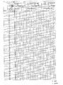
本実施形態に係る駆動方式は、1つの画素を複数のサブ画素に分割し、点灯しているサブ画素の数や面積を制御して階調を表現する面積階調方式と、1フレームを複数のサブフレームに分割し、各サブフレームに、発光回数や発光時間などの重み付けを行い、重み付けの総量を階調ごとに差を付けることによって階調を表現する時間階調方式を組み合わせるものである。つまり、1つの画素を、m個のサブ画素に分割し、m個のサブ画素の面積比を20:21:22:・・・・:2m−3:2m−2:2m−1とする。また、1フレームに、複数のサブフレームから構成されるk個(kはk≧2の整数)のサブフレーム群を設けるとともに、1フレームをn個のサブフレームに分割し、n個のサブフレームの点灯期間の長さの比を20:2m:22m:・・・・:2(n−3)m:2(n−2)m:2(n−1)mとする。さらに、n個の各サブフレームを、当該サブフレームの概ね1/kの長さの点灯期間を有するk個のサブフレームに分割し、k個の各サブフレーム群に1個ずつ配置する。このとき、k個のサブフレーム群で、サブフレームの出現順序が概ね同じになるように、サブフレームを配置する。そして、各サブフレームにおいてm個の各サブ画素の点灯のさせ方を制御することにより、階調を表現する。 In the driving method according to this embodiment, one pixel is divided into a plurality of sub-pixels, and an area gray scale method that expresses a gray scale by controlling the number and area of lighted sub-pixels and a plurality of one frame. Is divided into sub-frames, and each sub-frame is weighted such as the number of times of light emission and the light-emission time, and a time gray scale method that expresses a gray scale by differentiating the total weight for each gray scale is combined. . That is, one pixel is divided into m sub-pixel, the area ratio of the m sub-pixel 2 0: 2 1: 2 2 : ····: 2 m-3: 2 m-2: 2 Let m-1 . In addition, k subframe groups (k is an integer of k ≧ 2) composed of a plurality of subframes are provided in one frame, and one frame is divided into n subframes. The ratio of the length of the lighting period is 2 0 : 2 m : 2 2m :...: 2 (n-3) m : 2 (n-2) m : 2 (n-1) m . Further, each of the n subframes is divided into k subframes having a lighting period of approximately 1 / k of the subframe, and one subframe is arranged in each of the k subframe groups. At this time, the subframes are arranged so that the appearance order of the subframes is substantially the same in the k subframe groups. Then, gradation is expressed by controlling the lighting of the m sub-pixels in each sub-frame.
始めに、各階調の表現方法、つまり、各階調において、各サブフレームで各サブ画素をどのように点灯させるのかについて説明する。本実施形態では、1つの画素を、各サブ画素の面積比が1:2となるように、2個のサブ画素(SP1、SP2)に分割するとともに、1フレームに2個のサブフレーム群(SFG1、SFG2)を設け、1フレームを、各サブフレームの点灯期間の比率が1:4:16となるように、3個のサブフレーム(SF1、SF2、SF3)に分割した場合を例に挙げて説明する。なお、この例は、m=2、n=3、k=2に対応する。 First, an expression method of each gradation, that is, how each sub-pixel is lit in each sub-frame in each gradation will be described. In the present embodiment, one pixel is divided into two subpixels (SP1, SP2) such that the area ratio of each subpixel is 1: 2, and two subframe groups (one frame) ( SFG1, SFG2) are provided, and one frame is divided into three subframes (SF1, SF2, SF3) so that the ratio of the lighting periods of each subframe is 1: 4: 16. I will explain. This example corresponds to m = 2, n = 3, and k = 2.
ここで、各サブ画素の面積を、SP1=1、SP2=2、各サブフレームの点灯期間をSF1=1、SF2=4、SF3=16とする。 Here, the area of each sub-pixel is SP1 = 1, SP2 = 2, and the lighting period of each sub-frame is SF1 = 1, SF2 = 4, and SF3 = 16.
本実施形態では、点灯期間の比率が1:4:16となるように、1フレームを3個に分割して得られたサブフレーム(SF1〜SF3)のそれぞれを、当該サブフレームの1/2の長さの点灯期間を有する2個のサブフレームにさらに分割する。つまり、点灯期間1を有するSF1を、点灯期間0.5を有する2個のサブフレームSF11、SF21に分割する。同様に、点灯期間4を有するSF2を、点灯期間2を有する2個のサブフレームSF12、SF22に分割し、点灯期間16を有するSF3を、点灯期間8を有する2個のサブフレームSF13、SF23に分割する。そして、SF11、SF12、SF13をサブフレーム群1(SFG1)に、SF21、SF22、SF23をサブフレーム群2(SFG2)に配置する。このとき、サブフレーム群1とサブフレーム群2とで、SF11、SF12、SF13とSF21、SF22、SF23の出現順序を同じにする。
In this embodiment, each of the subframes (SF1 to SF3) obtained by dividing one frame into three so that the ratio of the lighting period is 1: 4: 16 is reduced to 1/2 of the subframe. Is further divided into two subframes having a lighting period of a length of. That is, SF1 having the
これにより、2個の各サブフレーム群はそれぞれ3個のサブフレームから構成され、各サブフレームの点灯期間はSF11=0.5、SF12=2、SF13=8、SF21=0.5、SF22=2、SF23=8となる。 Thus, each of the two subframe groups is composed of three subframes, and the lighting period of each subframe is SF11 = 0.5, SF12 = 2, SF13 = 8, SF21 = 0.5, SF22 = 2, SF23 = 8.
この場合の各階調の表現方法を図1に示す。なお、図1の見方として、各サブフレームにおいて○印がついているサブ画素は点灯し、×印がついているサブ画素は非点灯であることを示している。 A representation method of each gradation in this case is shown in FIG. In addition, as a way of viewing FIG. 1, in each subframe, the subpixels marked with ◯ are lit and the subpixels marked with x are not lit.
本発明では、各サブ画素の面積と各サブフレームの点灯期間の積を、実質的な発光強度と考える。例えば、サブフレーム群1において、点灯期間0.5を有するSF11では、面積1のサブ画素1のみが点灯した場合の発光強度は1×0.5=0.5となり、面積2のサブ画素2のみが点灯した場合の発光強度は2×0.5=1となる。同様に、点灯期間2を有するSF12では、サブ画素1のみが点灯した場合の発光強度は2となり、サブ画素2のみが点灯した場合の発光強度は4となる。同様に、点灯期間8を有するSF13では、サブ画素1のみが点灯した場合の発光強度は8となり、サブ画素2のみが点灯した場合の発光強度は16となる。なお、サブフレーム群2を構成するサブフレームでも同様に発光強度が定められる。このように、サブ画素の面積とサブフレームの点灯期間の組合せによって、異なる発光強度を作り出すことができ、この発光強度でもって階調を表現する。
In the present invention, the product of the area of each sub-pixel and the lighting period of each sub-frame is considered as a substantial light emission intensity. For example, in SF11 having a lighting period of 0.5 in
次に、階調の表現方法、つまり、各サブフレームの選択方法の一例について述べる。特に、点灯期間の長さが等しいサブフレームに関して、サブフレームの選択に次のような規則性がある方が望ましい。 Next, an example of a gradation expression method, that is, a method for selecting each subframe will be described. In particular, regarding subframes having the same lighting period length, it is desirable that the subframe selection has the following regularity.
例えば、点灯期間0.5を有するサブフレームSF11とSF21については、選択・非選択の状態を一致させるとともに、サブ画素の点灯・非点灯の状態も一致させる。つまり、SF11を選択すればSF21も選択し、SF11を選択しなければSF21も選択しない。また、例えば、SF11でサブ画素1が点灯すればSF21でもサブ画素1を点灯させ、SF11でサブ画素2が点灯すればSF21でもサブ画素2を点灯させる。なぜなら、元来は点灯期間が1のサブフレームであり、それをSF11とSF21に分割しただけであるからである。同様に、点灯期間2を有するサブフレームSF12とSF22も選択・非選択の状態を一致させるとともに、サブ画素の点灯・非点灯の状態も一致させる。なぜなら、SF12とSF22は元来点灯期間が4のサブフレームを分割したものであるからである。同様に、点灯期間8を有するサブフレームSF13とSF23も選択・非選択の状態を一致させるとともに、サブ画素の点灯・非点灯の状態も一致させる。なぜなら、SF13とSF23は元来点灯期間が16のサブフレームを分割したものであるからである。
For example, for the subframes SF11 and SF21 having the lighting period 0.5, the selected / non-selected states are matched, and the lighting / non-lit states of the subpixels are also matched. That is, if SF11 is selected, SF21 is also selected. If SF11 is not selected, SF21 is not selected. Further, for example, if the
このため、例えば、階調1を表現する場合は、SF11とSF21とでサブ画素1を点灯させる。また、階調2を表現する場合は、SF11とSF21とでサブ画素2を点灯させる。また、階調3を表現する場合は、SF11とSF21とでサブ画素1とサブ画素2を点灯させる。また、階調6を表現する場合は、SF11とSF21とでサブ画素2を点灯させ、SF12とSF22とでサブ画素1を点灯させる。その他の階調についても同様に、各サブフレームで点灯させる各サブ画素を選択する。
For this reason, for example, when the
以上のように、各サブフレームで点灯させるサブ画素を選択することにより、6ビット階調(64階調)を表現することができる。 As described above, 6-bit gradation (64 gradations) can be expressed by selecting a subpixel to be lit in each subframe.
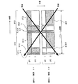
本発明の駆動方式を用いると、擬似輪郭を低減させることができる。例えば、図1において、画素Aでは、階調31を表示し、画素Bでは、階調32で表示しているとする。その場合の、各サブフレームにおける各サブ画素の点灯・非点灯の状態を、図2に示す。
When the driving method of the present invention is used, the pseudo contour can be reduced. For example, in FIG. 1, it is assumed that
ここで、図2の見方を説明する。図2は、1フレームでの画素の点灯・非点灯の状態を示す図である。図2の横方向は時間を示し、縦方向は画素の位置を示している。そして、図2に示された四角形の縦方向の長さが、各サブ画素の面積比を示し、横方向の長さが、各サブフレームの点灯期間の長さの比を示している。また、図2に描かれたそれぞれの四角形の面積が、発光強度を示している。 Here, how to view FIG. 2 will be described. FIG. 2 is a diagram showing a state of lighting / non-lighting of pixels in one frame. The horizontal direction in FIG. 2 indicates time, and the vertical direction indicates the pixel position. The vertical length of the quadrangle shown in FIG. 2 indicates the area ratio of each sub-pixel, and the horizontal length indicates the ratio of the length of the lighting period of each sub-frame. Further, the area of each quadrangle depicted in FIG. 2 indicates the emission intensity.
例えば、視線が動いたとすると、視線の追い方によって、あるときは階調が26(=2+8+16)と感じ、あるときは、階調が29(=16+1+4+8)と感じる。本来は、階調が31と32に見えるべきであるのに、階調が26や29に見えてしまい、擬似輪郭が発生してしまう。しかし、階調のずれが従来の駆動方式よりも小さくなるため、従来の駆動方式を用いるよりも擬似輪郭が低減される。 For example, if the line of sight moves, depending on how the line of sight is followed, the gray level is felt 26 (= 2 + 8 + 16) in some cases, and the gray level is felt 29 (= 16 + 1 + 4 + 8) in some cases. Originally, the gradation should be seen as 31 and 32, but the gradation is seen as 26 or 29, and a pseudo contour is generated. However, since the gradation shift is smaller than that of the conventional driving method, the pseudo contour is reduced as compared with the case of using the conventional driving method.
なお、本実施形態では、サブフレーム群と同じ個数に分割する前のサブフレーム(SF1、SF2、SF3)の点灯期間の長さは1、4、16であるとしたが、これに限定されない。 In this embodiment, the length of the lighting period of the subframes (SF1, SF2, SF3) before being divided into the same number as the subframe group is 1, 4, and 16, but the present invention is not limited to this.
また、本実施形態では、点灯期間の比率が1:4:16である3個のサブフレーム(SF1、SF2、SF3)のそれぞれを、さらに、サブフレーム群の個数と同じ2個のサブフレーム(SF11〜SF23)に分割したが、各サブフレームの分割数は、サブフレーム群の個数と異なっていてもよい。 In this embodiment, each of the three subframes (SF1, SF2, SF3) having a lighting period ratio of 1: 4: 16 is further divided into two subframes (the same number of subframe groups). Although divided into SF11 to SF23), the number of divisions of each subframe may be different from the number of subframe groups.
例えば、点灯期間の長さの比が20:2m:22m:・・・・:2(n−3)m:2(n−2)m:2(n−1)mであるn個のサブフレームのうち少なくとも1個のサブフレームを、当該サブフレームの概ね1/(a×k)(aはa≧2の整数)の長さの点灯期間を有する(a×k)個のサブフレームに分割し、k個の各サブフレーム群にa個ずつ配置し、残りのサブフレームを、当該サブフレームの概ね1/kの長さの点灯期間を有するk個のサブフレームに分割し、k個の各サブフレーム群に1個ずつ配置してもよい。特に、点灯期間を(a×k)個のサブフレームに分割するサブフレームとして、n個のサブフレームのうち最長の点灯期間を有するサブフレームを選択してもよい。 For example, the ratio of the length of the lighting period is 2 0 : 2 m : 2 2m :...: 2 (n−3) m : 2 (n−2) m : 2 (n−1) m At least one subframe of the subframes has (a × k) lighting periods having a lighting period of approximately 1 / (a × k) (a is an integer of a ≧ 2). Divide into subframes, arrange a in each of the k subframe groups, and divide the remaining subframes into k subframes having a lighting period of approximately 1 / k of the subframe. , One may be arranged in each of the k subframe groups. In particular, as a subframe that divides the lighting period into (a × k) subframes, a subframe having the longest lighting period among n subframes may be selected.
例えば、1つの画素を、各サブ画素の面積比が1:2となるように、2個のサブ画素(SP1、SP2)に分割するとともに、1フレームに2個のサブフレーム群(SFG1、SFG2)を設け、1フレームを点灯期間の比率が1:4:16となるように3個のサブフレーム(SF1、SF2、SF3)に分割し、その中で最長の点灯期間16を有するサブフレームを、当該サブフレームの1/4の長さの点灯期間を有する4個のサブフレームに分割し、残りの2個のサブフレームを、当該サブフレームの1/2の長さの点灯期間を有する2個のサブフレームに分割した場合の例を、図3に示す。なお、この例は、m=2、n=3、k=2、a=2に対応する。
For example, one pixel is divided into two subpixels (SP1, SP2) such that the area ratio of each subpixel is 1: 2, and two subframe groups (SFG1, SFG2) are included in one frame. ) Is divided into three subframes (SF1, SF2, SF3) such that the ratio of the lighting period is 1: 4: 16, and the subframe having the
ここで、各サブ画素の面積を、SP1=1、SP2=2、各サブフレームの点灯期間をSF1=1、SF2=4、SF3=16とする。 Here, the area of each sub-pixel is SP1 = 1, SP2 = 2, and the lighting period of each sub-frame is SF1 = 1, SF2 = 4, and SF3 = 16.
図3では、点灯期間の比率が1:4:16となるように1フレームを3個に分割して得られたサブフレームのうち、最長の点灯期間16を有するSF3を、当該サブフレームの1/4の長さの点灯期間4を有する4個のサブフレームSF13、SF14、SF23、SF24に分割する。また、残りのSF1、SF2については、当該サブフレームの1/2の長さの点灯期間を有する2個のサブフレームにさらに分割する。つまり、点灯期間1を有するSF1を、点灯期間0.5を有する2個のサブフレームSF11、SF21に分割し、点灯期間4を有するSF2を、点灯期間2を有する2個のサブフレームSF12、SF22に分割する。そして、SF11、SF12、SF13、SF14をサブフレーム群1(SFG1)に、SF21、SF22、SF23、SF24をサブフレーム群2(SFG2)に配置する。このとき、サブフレーム群1とサブフレーム群2とで、SF11、SF12、SF13、SF14とSF21、SF22、SF23、SF24の出現順序を同じにする。
In FIG. 3, among subframes obtained by dividing one frame into three so that the ratio of the lighting periods is 1: 4: 16, SF3 having the
これにより、2個の各サブフレーム群はそれぞれ4個のサブフレームから構成され、各サブフレームの点灯期間はSF11=0.5、SF12=2、SF13=4、SF14=4、SF21=0.5、SF22=2、SF23=4、SF24=4となる。 Thus, each of the two subframe groups is composed of four subframes, and the lighting periods of each subframe are SF11 = 0.5, SF12 = 2, SF13 = 4, SF14 = 4, SF21 = 0. 5, SF22 = 2, SF23 = 4, and SF24 = 4.
図3において、各サブ画素の面積と各サブフレームの点灯期間の積を、実質的な発光強度と考える。例えば、サブフレーム群1において、点灯期間0.5を有するSF11では、面積1のサブ画素1のみが点灯した場合の発光強度は0.5となり、面積2のサブ画素2のみが点灯した場合の発光強度は1となる。同様に、点灯期間2を有するSF12では、サブ画素1のみが点灯した場合の発光強度は2となり、サブ画素2のみが点灯した場合の発光強度は4となる。同様に、点灯期間4を有するSF13、SF14では、サブ画素1のみが点灯した場合の発光強度は4となり、サブ画素2のみが点灯した場合の発光強度は8となる。なお、サブフレーム群2を構成するサブフレームでも同様に発光強度が定められる。このように、サブ画素の面積とサブフレームの点灯期間の組合せによって、異なる発光強度を作り出すことができ、この発光強度でもって6ビット階調(64階調)を表現する。
In FIG. 3, the product of the area of each sub-pixel and the lighting period of each sub-frame is considered as a substantial light emission intensity. For example, in SF11 having a lighting period of 0.5 in
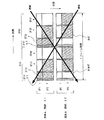
図3のような駆動方式を用いて、擬似輪郭を低減させることができる。例えば、図3において、画素Aでは、階調31を表示し、画素Bでは、階調32で表示しているとする。その場合の、各サブフレームにおける各サブ画素の点灯・非点灯の状態を、図4に示す。例えば、視線が動いたとすると、視線の追い方によって、あるときは階調が22(=2+4+8+8)と感じ、あるときは、階調が29(=8+8+1+4+4+4)と感じる。本来は、階調が31と32に見えるべきであるのに、階調が22や29に見えてしまい、擬似輪郭が発生してしまう。しかし、階調のずれが従来の駆動方式よりも小さくなるため、従来の駆動方式よりも擬似輪郭が低減される。
The pseudo contour can be reduced by using the driving method as shown in FIG. For example, in FIG. 3, it is assumed that
このように、各サブフレームの点灯期間をより短くしたり、サブフレームの分割数を増やすことにより、視線が動いた場合の階調のずれが従来の駆動方式よりも小さく感じる様に目が誤魔化される。したがって、擬似輪郭を低減させる効果が大きくなる。なお、点灯期間をさらに4個に分割するサブフレームは、最長の点灯期間を有するサブフレームに限定されない。 In this way, by shortening the lighting period of each sub-frame or increasing the number of sub-frame divisions, the eyes are misled so that the gradation shift when the line of sight moves is felt smaller than in the conventional driving method. It is. Therefore, the effect of reducing the pseudo contour is increased. Note that the subframe in which the lighting period is further divided into four is not limited to the subframe having the longest lighting period.
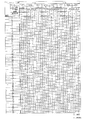
なお、各サブフレームの点灯期間をより短くしたり、分割数を増やすことにより、同じ階調を表現するための各サブフレームにおけるサブ画素の選択方法が増える。したがって、各サブフレームにおける各サブ画素の選択方法は、これに限定されない。例えば、階調31を表現する場合、図3では、SF13、SF14、SF23、SF24でサブ画素1を点灯させていたが、SF13及びSF23でサブ画素2を点灯させてもよい。この場合の例を図5に示す。
Note that, by shortening the lighting period of each subframe or increasing the number of divisions, the number of subpixel selection methods in each subframe for expressing the same gradation is increased. Therefore, the selection method of each sub-pixel in each sub-frame is not limited to this. For example, when the
なお、図5のような駆動方式を用いて、擬似輪郭を低減させることができる。例えば、図5において、画素Aでは、階調31を表示し、画素Bでは、階調32で表示しているとする。その場合の、各サブフレームにおける各サブ画素の点灯・非点灯の状態を、図6に示す。例えば、視線が動いたとすると、視線の追い方によって、あるときは階調が26(=2+8+8+8)と感じ、あるときは、階調が29(=8+8+1+4+8)と感じる。本来は、階調が31と32に見えるべきであるのに、階調が26や29に見えてしまい、擬似輪郭が発生してしまう。しかし、階調のずれが従来の駆動方式よりも小さくなるため、従来の駆動方式よりも擬似輪郭が低減される。
Note that the pseudo contour can be reduced by using a driving method as shown in FIG. For example, in FIG. 5, it is assumed that
このように、擬似輪郭が特に出やすい階調に対して、選択的に各サブフレームにおけるサブ画素の選択方法を変えることにより、擬似輪郭を低減させる効果を大きくすることができる。 As described above, the effect of reducing the pseudo contour can be increased by selectively changing the selection method of the sub-pixels in each sub-frame with respect to the gradation in which the pseudo contour is particularly likely to appear.
なお、各サブフレームの点灯期間の順序は、これに限定されない。例えば、各サブフレーム群の中で点灯期間の昇順もしくは降順としてもよい。なぜならば、各サブフレームの点灯期間の順序を点灯期間の昇順もしくは降順とすることにより、視線を動かしたときの階調のずれを、従来の駆動方式よりもより小さくすることができるため、従来の駆動方式よりも擬似輪郭をより低減できるからである。 Note that the order of the lighting periods of the subframes is not limited to this. For example, the lighting periods may be in ascending order or descending order in each subframe group. This is because the gradation shift when moving the line of sight can be made smaller than in the conventional driving method by setting the lighting period of each subframe in ascending or descending order of the lighting period. This is because the pseudo contour can be further reduced as compared with this driving method.
もしくは、各サブフレーム群の中で点灯期間の昇順もしくは降順に配置した後、最長の点灯期間を有するサブフレームと2番目に長い点灯期間を有するサブフレームの順序を入れ換えてもよい。 Alternatively, after arranging the lighting periods in ascending or descending order in each subframe group, the order of the subframe having the longest lighting period and the subframe having the second longest lighting period may be interchanged.
例えば、図5において、各サブフレーム群の中で最長の点灯期間を有するサブフレームと2番目に長い点灯期間を有するサブフレームの順序を入れ換えた場合の例を、図7に示す。 For example, FIG. 7 shows an example in which the order of the subframe having the longest lighting period and the subframe having the second longest lighting period in each subframe group is switched in FIG.
図7では、図5において、各サブフレーム群の中で最長の点灯期間4を有するサブフレームと2番目に長い点灯期間2を有するサブフレームの順序を入れ換えている。つまり、サブフレーム群1においては、点灯期間4を有するSF13と点灯期間2を有するSF12を入れ換えており、サブフレーム群2においては、点灯期間4を有するSF23と点灯期間2を有するSF22を入れ換えている。
7, the order of the subframe having the
なお、図7のような駆動方式を用いて、擬似輪郭を低減させることができる。例えば、図7において、画素Aでは、階調31を表示し、画素Bでは、階調32で表示しているとする。その場合の、各サブフレームにおける各サブ画素の点灯・非点灯の状態を、図8に示す。例えば、視線が動いたとすると、視線の追い方によって、あるときは階調が28(=8+4+8+8)と感じ、あるときは、階調が30(=8+8+8+4+2)と感じる。本来は、階調が31と32に見えるべきであるのに、階調が28や30に見えてしまい、擬似輪郭が発生してしまう。しかし、階調のずれが従来の駆動方式よりも小さくなるため、従来の駆動方式よりも擬似輪郭が低減される。
Note that the pseudo contour can be reduced by using a driving method as shown in FIG. For example, in FIG. 7, it is assumed that
このように、各サブフレームの点灯期間の順序を変えることにより、目が誤魔化され、視線が動いたときの階調のずれを小さくすることができる。よって、擬似輪郭を低減させることができる。 In this way, by changing the order of the lighting periods of the sub-frames, it is possible to reduce the gray level shift when the eyes are misled and the line of sight moves. Therefore, the pseudo contour can be reduced.
なお、各サブフレーム群の中で点灯期間の昇順もしくは降順に配置した後、順序を入れ換えるサブフレームは、最長の点灯期間を有するサブフレームと2番目に長い点灯期間を有するサブフレームに限定されない。例えば、最長の点灯期間を有するサブフレームと3番目に長い点灯期間を有するサブフレームを入れ換えてもよいし、2番目に長い点灯期間を有するサブフレームと3番目に長い点灯期間を有するサブフレームを入れ換えてもよい。 Note that the subframes in which the order is switched after the lighting periods are arranged in ascending or descending order in each subframe group are not limited to the subframe having the longest lighting period and the subframe having the second longest lighting period. For example, the subframe having the longest lighting period and the subframe having the third longest lighting period may be interchanged, and the subframe having the second longest lighting period and the subframe having the third longest lighting period may be replaced. It may be replaced.
なお、点灯期間の長さは、全体の階調数(ビット数)や全体のサブフレーム数などにより、適宜変わるものである。よって、点灯期間の長さが同じであっても、全体の階調数(ビット数)や全体のサブフレーム数が変われば、実際に点灯している期間の長さ(例えば、何μsであるか)が変わる可能性がある。 Note that the length of the lighting period varies depending on the total number of gradations (number of bits), the total number of subframes, and the like. Therefore, even if the length of the lighting period is the same, if the total number of gradations (number of bits) or the total number of subframes changes, the length of the actual lighting period (for example, how many μs it is) ) May change.
なお、点灯期間は、ずっと点灯し続ける場合に用いるものであり、点灯回数は、ある時間内において、点滅し続ける場合に用いるものである。点灯回数を用いる代表的なディスプレイは、プラズマディスプレイである。点灯期間を用いる代表的なディスプレイは、有機ELディスプレイである。 The lighting period is used when the lamp continues to be lit, and the lighting count is used when the lamp continues to flash within a certain time. A typical display using the number of times of lighting is a plasma display. A typical display using the lighting period is an organic EL display.
なお、本実施形態では、各サブ画素の面積比は1:2としていたが、これに限定されない。例えば、1:4に分割してもよいし、1:8に分割してもよい。 In this embodiment, the area ratio of each sub-pixel is 1: 2, but is not limited to this. For example, it may be divided into 1: 4 or 1: 8.
例えば、各サブ画素の面積比を1:1とすると、同じサブフレームでどちらのサブ画素を発光させても発光強度は等しくなる。したがって、同じ階調を表現する際に、どちらのサブ画素を発光させるかを切り換えてもよい。これにより、特定のサブ画素のみ集中して発光することを防ぐことができ、画素の焼き付きを防止できる。 For example, if the area ratio of each sub-pixel is 1: 1, the light emission intensity is equal regardless of which sub-pixel emits light in the same sub-frame. Therefore, when expressing the same gradation, it may be switched which sub-pixel emits light. As a result, it is possible to prevent only specific sub-pixels from emitting light in a concentrated manner, and to prevent pixel burn-in.
なお、m個のサブ画素の面積比を20:21:22:・・・・:2m−3:2m−2:2m−1とし、n個のサブフレームの点灯期間の長さの比を20:2m:22m:・・・・:2(n−3)m:2(n−2)m:2(n−1)mとすることにより、少ないサブ画素数及び少ないサブフレーム数で、より多くの階調を表現することが可能となる。また、この方法で表現できる階調は、階調の変化率が一定となるため、よりなめらかな階調表示が可能となり、画質を向上させることができる。 Incidentally, the area ratio of the m sub-pixel 2 0: 2 1: 2 2 : ····: 2 m-3: 2 m-2: 2 and m-1, the lighting period of the n sub-frame By setting the length ratio to 2 0 : 2 m : 2 2m :...: 2 (n-3) m : 2 (n-2) m : 2 (n-1) m , fewer subpixels More gradations can be expressed with a smaller number and a smaller number of subframes. In addition, since the gradation that can be expressed by this method has a constant gradation change rate, smoother gradation display is possible and image quality can be improved.
なお、本実施形態では、サブ画素の数は2個としていたが、これに限定されない。 In the present embodiment, the number of sub-pixels is two, but the present invention is not limited to this.
例えば、1つの画素を、各サブ画素の面積比が1:2:4となるように、3個のサブ画素(SP1、SP2、SP3)に分割するとともに、1フレームに2個のサブフレーム群(SFG1、SFG2)を設け、1フレームを、各サブフレームの点灯期間の比率が1:8となるように、2個のサブフレーム(SF1、SF2)に分割した場合の例を、図9に示す。なお、この例は、m=3、n=2、k=2に対応する。 For example, one pixel is divided into three subpixels (SP1, SP2, SP3) so that the area ratio of each subpixel is 1: 2: 4, and two subframe groups are included in one frame. FIG. 9 shows an example in which (SFG1, SFG2) is provided and one frame is divided into two subframes (SF1, SF2) such that the ratio of the lighting period of each subframe is 1: 8. Show. This example corresponds to m = 3, n = 2, and k = 2.
ここで、各サブ画素の面積を、SP1=1、SP2=2、SP3=4、各サブフレームの点灯期間をSF1=1、SF2=8とする。 Here, the area of each subpixel is SP1 = 1, SP2 = 2, SP3 = 4, and the lighting period of each subframe is SF1 = 1 and SF2 = 8.
図9では、点灯期間の比率が1:8となるように1フレームを2個に分割して得られたサブフレーム(SF1、SF2)のそれぞれを、当該サブフレーム(SF1、SF2)の1/2の長さの点灯期間を有する2個のサブフレームにさらに分割する。つまり、点灯期間1を有するSF1を、点灯期間0.5を有する2個のサブフレームSF11、SF21に分割する。同様に、点灯期間8を有するSF2を、点灯期間4を有する2個のサブフレームSF12、SF22に分割する。そして、SF11、SF12をサブフレーム群1(SFG1)に、SF21、SF22をサブフレーム群2(SFG2)に配置する。このとき、サブフレーム群1とサブフレーム群2とで、SF11、SF12とSF21、SF22の出現順序を同じにする。
In FIG. 9, each of the subframes (SF1, SF2) obtained by dividing one frame into two so that the ratio of the lighting period is 1: 8 is represented by 1 / of the subframe (SF1, SF2). It is further divided into two subframes having a lighting period of 2 lengths. That is, SF1 having the
これにより、2個の各サブフレーム群はそれぞれ2個のサブフレームから構成され、各サブフレームの点灯期間はSF11=0.5、SF12=4、SF21=0.5、SF22=4となる。 Thus, each of the two subframe groups is composed of two subframes, and the lighting periods of each subframe are SF11 = 0.5, SF12 = 4, SF21 = 0.5, and SF22 = 4.
図9において、各サブ画素の面積と各サブフレームの点灯期間の積を、実質的な発光強度と考える。例えば、サブフレーム群1において、点灯期間0.5を有するSF11では、面積1のサブ画素1のみが点灯した場合の発光強度は0.5となり、面積2のサブ画素2のみが点灯した場合の発光強度は1となり、面積4のサブ画素3のみが点灯した場合の発光強度は2となる。同様に、点灯期間4を有するSF12では、サブ画素1のみが点灯した場合の発光強度は4となり、サブ画素2のみが点灯した場合の発光強度は8となり、サブ画素3のみが点灯した場合の発光強度は16となる。なお、サブフレーム群2を構成するサブフレームでも同様に発光強度が定められる。このように、サブ画素の面積とサブフレームの点灯期間の組合せによって、異なる発光強度を作り出すことができ、この発光強度でもって6ビット階調(64階調)を表現する。
In FIG. 9, the product of the area of each sub-pixel and the lighting period of each sub-frame is considered as a substantial light emission intensity. For example, in SF11 having a lighting period of 0.5 in
図9のような駆動方式を用いて、擬似輪郭を低減させることができる。例えば、図9において、画素Aでは、階調31を表示し、画素Bでは、階調32で表示しているとする。その場合の、各サブフレームにおける各サブ画素の点灯・非点灯の状態を、図10に示す。例えば、視線が動いたとすると、視線の追い方によって、あるときは階調が28.5(=0.5+4+8+16)と感じ、あるときは、階調が30(=16+2+8+4)と感じる。本来は、階調が31と32に見えるべきであるのに、階調が28.5や30に見えてしまい、擬似輪郭が発生してしまう。しかし、階調のずれが従来の駆動方式よりも小さくなるため、従来の駆動方式を用いるよりも擬似輪郭が低減される。
The pseudo contour can be reduced by using the driving method as shown in FIG. For example, in FIG. 9, it is assumed that
また、図9において、1フレームを点灯期間の比率が1:8となるように2個のサブフレーム(SF1、SF2)に分割し、その中で最長の点灯期間8を有するサブフレームを、当該サブフレームの1/4の長さの点灯期間を有する4個のサブフレームに分割し、残りのサブフレームを、当該サブフレームの1/2の長さの点灯期間を有する2個のサブフレームに分割してもよい。この場合の例を、図11に示す。なお、この例は、m=3、n=2、k=2、a=2に対応する。
Further, in FIG. 9, one frame is divided into two subframes (SF1, SF2) so that the ratio of the lighting period is 1: 8, and the subframe having the
ここで、各サブ画素の面積を、SP1=1、SP2=2、SP3=4、各サブフレームの点灯期間をSF1=1、SF2=8とする。 Here, the area of each subpixel is SP1 = 1, SP2 = 2, SP3 = 4, and the lighting period of each subframe is SF1 = 1 and SF2 = 8.
図11では、点灯期間の比率が1:8となるように1フレームを2個に分割して得られたサブフレームのうち、最長の点灯期間8を有するSF2を、当該サブフレームの1/4の長さの点灯期間2を有する4個のサブフレームSF12、SF13、SF22、SF23に分割する。また、残りのSF1については、当該サブフレームの1/2の長さの点灯期間0.5を有する2個のサブフレームSF11、SF21にさらに分割する。そして、SF11、SF12、SF13をサブフレーム群1(SFG1)に、SF21、SF22、SF23をサブフレーム群2(SFG2)に配置する。このとき、サブフレーム群1とサブフレーム群2とで、SF11、SF12、SF13とSF21、SF22、SF23の出現順序を同じにする。
In FIG. 11, among the subframes obtained by dividing one frame into two so that the ratio of the lighting periods is 1: 8, SF2 having the
これにより、2個の各サブフレーム群はそれぞれ3個のサブフレームから構成され、各サブフレームの点灯期間はSF11=0.5、SF12=2、SF13=2、SF21=0.5、SF22=2、SF23=2となる。 Thus, each of the two subframe groups is composed of three subframes, and the lighting period of each subframe is SF11 = 0.5, SF12 = 2, SF13 = 2, SF21 = 0.5, SF22 = 2, SF23 = 2.
図11において、各サブ画素の面積と各サブフレームの点灯期間の積を、実質的な発光強度と考える。例えば、サブフレーム群1において、点灯期間0.5を有するSF11では、面積1のサブ画素1のみが点灯した場合の発光強度は0.5となり、面積2のサブ画素2のみが点灯した場合の発光強度は1となり、面積4のサブ画素3のみが点灯した場合の発光強度は2となる。同様に、点灯期間2を有するSF12、SF13では、サブ画素1のみが点灯した場合の発光強度は2となり、サブ画素2のみが点灯した場合の発光強度は4となり、サブ画素3のみが点灯した場合の発光強度は8となる。なお、サブフレーム群2を構成するサブフレームでも同様に発光強度が定められる。このように、サブ画素の面積とサブフレームの点灯期間の組合せによって、異なる発光強度を作り出すことができ、この発光強度でもって6ビット階調(64階調)を表現する。
In FIG. 11, the product of the area of each sub-pixel and the lighting period of each sub-frame is considered as a substantial light emission intensity. For example, in SF11 having a lighting period of 0.5 in
図11のような駆動方式を用いて、擬似輪郭を低減させることができる。例えば、図11において、画素Aでは、階調31を表示し、画素Bでは、階調32で表示しているとする。その場合の、各サブフレームにおける各サブ画素の点灯・非点灯の状態を、図12に示す。例えば、視線が動いたとすると、視線の追い方によって、あるときは階調が22(=2+4+8+8)と感じ、あるときは、階調が28(=8+8+2+4+4+2)と感じる。本来は、階調が31と32に見えるべきであるのに、階調が22や28に見えてしまい、擬似輪郭が発生してしまう。しかし、階調のずれが従来の駆動方式よりも小さくなるため、従来の駆動方式よりも擬似輪郭が低減される。
The pseudo contour can be reduced by using the driving method as shown in FIG. For example, in FIG. 11, it is assumed that
このように、各サブフレームの点灯期間をより短くしたり、サブフレームの分割数を増やすことにより、目が誤魔化され、視線が動いた場合の階調のずれが従来の駆動方式よりも小さくなる。したがって、擬似輪郭を低減させる効果が大きくなる。なお、点灯期間をさらに4個に分割するサブフレームは、最長の点灯期間を有するサブフレームに限定されない。 In this way, by shortening the lighting period of each subframe or increasing the number of subframe divisions, the eyes become misleading and the gradation shift when the line of sight moves is smaller than in the conventional driving method. . Therefore, the effect of reducing the pseudo contour is increased. Note that the subframe in which the lighting period is further divided into four is not limited to the subframe having the longest lighting period.
なお、各サブフレームの点灯期間をより短くしたり、分割数を増やすことにより、同じ階調を表現するための各サブフレームにおけるサブ画素の選択方法が増える。したがって、各サブフレームにおける各サブ画素の選択方法は、これに限定されない。例えば、階調31を表現する場合、図11では、SF12、SF13、SF22、SF23でサブ画素1及びサブ画素2を点灯させていたが、SF12及びSF22でサブ画素2及びサブ画素3を点灯させてもよい。この場合の例を図13に示す。
Note that, by shortening the lighting period of each subframe or increasing the number of divisions, the number of subpixel selection methods in each subframe for expressing the same gradation is increased. Therefore, the selection method of each sub-pixel in each sub-frame is not limited to this. For example, in the case of expressing
なお、図13のような駆動方式を用いて、擬似輪郭を低減させることができる。例えば、図13において、画素Aでは、階調31を表示し、画素Bでは、階調32で表示しているとする。その場合の、各サブフレームにおける各サブ画素の点灯・非点灯の状態を、図14に示す。例えば、視線が動いたとすると、視線の追い方によって、あるときは階調が28(=4+8+8+8)と感じ、あるときは、階調が30(=8+8+2+8+4)と感じる。本来は、階調が31と32に見えるべきであるのに、階調が28や30に見えてしまい、擬似輪郭が発生してしまう。しかし、階調のずれが従来の駆動方式よりも小さくなるため、従来の駆動方式よりも擬似輪郭が低減される。
Note that the pseudo contour can be reduced by using a driving method as shown in FIG. For example, in FIG. 13, it is assumed that
このように、擬似輪郭が特に出やすい階調に対して、選択的に各サブフレームにおけるサブ画素の選択方法を変えることにより、擬似輪郭を低減させる効果を大きくすることができる。 As described above, the effect of reducing the pseudo contour can be increased by selectively changing the selection method of the sub-pixels in each sub-frame with respect to the gradation in which the pseudo contour is particularly likely to appear.
なお、サブ画素の番号と面積の対応は、これに限定されない。例えば、図11において、各サブ画素の面積をSP1=1、SP2=2、SP3=4としたが、SP1=1、SP2=4、SP3=2としてもよいし、SP1=2、SP2=1、SP3=4としてもよいし、SP1=4、SP2=2、SP3=1としてもよい。 Note that the correspondence between the subpixel number and the area is not limited to this. For example, in FIG. 11, the area of each sub-pixel is SP1 = 1, SP2 = 2, and SP3 = 4. However, SP1 = 1, SP2 = 4, and SP3 = 2 may be used, or SP1 = 2 and SP2 = 1. SP3 = 4, or SP1 = 4, SP2 = 2, or SP3 = 1.
このように、本発明の駆動方式を用いることにより、サブフレーム数を多くせずに、擬似輪郭を低減したり、階調数を大きくして表示させることが可能となる。また、従来の時間階調方式に比べて、サブフレームの個数を少なくすることができるため、各サブフレーム期間を長く設けることができる。これにより、デューティー比を向上させることができ、発光素子にかかる電圧が小さくなる。したがって、消費電力を低減でき、発光素子の劣化も少なくなる。 In this manner, by using the driving method of the present invention, it is possible to reduce the pseudo contour or increase the number of gradations without increasing the number of subframes. In addition, since the number of subframes can be reduced as compared with the conventional time gray scale method, each subframe period can be provided longer. Thereby, the duty ratio can be improved and the voltage applied to the light emitting element is reduced. Therefore, power consumption can be reduced and deterioration of the light emitting element is also reduced.
なお、ある階調において、各サブフレームにおけるサブ画素の選択方法を時間的に、または、場所的に変更してもよい。つまり、時刻によって、各サブフレームにおけるサブ画素の選択方法を変えてもよいし、画素によって、各サブフレームにおけるサブ画素の選択方法を変えてもよい。さらに、時刻によって変えて、かつ、画素によっても変えてもよい。 Note that, in a certain gradation, the selection method of subpixels in each subframe may be changed in time or place. That is, the subpixel selection method in each subframe may be changed depending on the time, or the subpixel selection method in each subframe may be changed depending on the pixel. Further, it may be changed depending on the time and also depending on the pixel.
例えば、ある階調を表現するとき、フレーム数が奇数番目のときと、偶数番目のときとで、各サブフレームにおけるサブ画素の選択方法を変えてもよい。例えば、フレーム数が奇数番目のときは、図11に示したサブ画素の選択方法で階調を表現し、偶数番目のときは、図13に示したサブ画素の選択方法で階調を表現してもよい。このように、擬似輪郭が特に出やすい階調に対するサブ画素の選択方法を、フレーム数が奇数番目のときと、偶数番目のときとで変えることにより、擬似輪郭を低減することができる。 For example, when expressing a certain gradation, the selection method of the sub-pixels in each sub-frame may be changed depending on whether the number of frames is an odd number or an even number. For example, when the number of frames is an odd number, gradation is expressed by the subpixel selection method shown in FIG. 11, and when the number is even, the gradation is expressed by the subpixel selection method shown in FIG. May be. As described above, the pseudo contour can be reduced by changing the selection method of the sub-pixel for the gradation at which the pseudo contour is particularly likely to appear between the odd number and the even number.
なお、ここでは、擬似輪郭が特に出やすい階調に対するサブフレームの選択方法を変えたが、任意の階調に対して、サブ画素の選択方法を変えてもよい。 Note that here, the subframe selection method is changed for gradations at which pseudo contours are particularly likely to appear, but the subpixel selection method may be changed for arbitrary gradations.
また、ある階調を表現するとき、奇数行目の画素を表示するときと、偶数行目の画素を表示するときとで、各サブフレームにおけるサブ画素の選択の仕方を変えてもよい。また、ある階調を表現するとき、奇数列目の画素を表示するときと、偶数列目の画素を表示するときとで、各サブフレームにおけるサブ画素の選択の仕方を変えてもよい。 In addition, when expressing a certain gradation, a method of selecting a sub pixel in each sub frame may be changed depending on whether an odd row pixel is displayed or an even row pixel is displayed. In addition, when expressing a certain gradation, a method of selecting a sub pixel in each sub frame may be changed depending on whether an odd column pixel is displayed or an even column pixel is displayed.
また、ある階調を表現するとき、フレーム数が奇数番目のときと、偶数番目のときとで、サブフレームの分割数や点灯期間の比率を変えてもよい。例えば、フレーム数が奇数番目のときは、図9で示したサブ画素の選択方法で階調を表現し、フレーム数が偶数番目のときは、図11で示したサブ画素の選択方法で階調を表現してもよい。 Further, when expressing a certain gradation, the number of subframe divisions and the ratio of the lighting period may be changed depending on whether the number of frames is an odd number or an even number. For example, when the number of frames is an odd number, gradation is expressed by the subpixel selection method shown in FIG. 9, and when the number of frames is an even number, the gradation is expressed by the subpixel selection method shown in FIG. May be expressed.
なお、各サブフレームの点灯期間の順序は、時刻によって変化してもよい。例えば、1フレーム目と2フレーム目とで、サブフレームの点灯期間の順序が変わってもよい。また、サブフレームの点灯期間の順序は、場所によって変わってもよい。例えば、画素Aと画素Bとで、サブフレームの点灯期間の順序が変わってもよい。また、それらを組み合わせて、サブフレームの点灯期間の順序が、時刻によって変化して、かつ、場所によって変化してもよい。例えば、図11において、フレーム数が奇数番目のときは、各サブフレームの点灯期間をSF11=0.5、SF12=2、SF13=2、SF21=0.5、SF22=2、SF23=2とし、フレーム数が偶数番目のときは、SF11=2、SF12=0.5、SF13=2、SF21=2、SF22=0.5、SF23=2としてもよい。 Note that the order of the lighting periods of the sub-frames may change depending on the time. For example, the order of the lighting periods of the subframes may be changed between the first frame and the second frame. Further, the order of the lighting periods of the subframes may be changed depending on the place. For example, the order of the lighting periods of the subframes may be changed between the pixel A and the pixel B. Further, by combining them, the order of the lighting periods of the subframes may change depending on the time and change depending on the place. For example, in FIG. 11, when the number of frames is an odd number, the lighting period of each subframe is set to SF11 = 0.5, SF12 = 2, SF13 = 2, SF21 = 0.5, SF22 = 2, and SF23 = 2. When the number of frames is an even number, SF11 = 2, SF12 = 0.5, SF13 = 2, SF21 = 2, SF22 = 0.5, and SF23 = 2 may be set.
なお、これまでは、サブフレーム群の個数が2個(k=2)の場合の例を示してきたが、サブフレーム群の個数はこれに限定されない。例えば、1フレームに4個のサブフレーム群を設けた場合の例を図15に示す。 Heretofore, an example in which the number of subframe groups is two (k = 2) has been shown, but the number of subframe groups is not limited to this. For example, FIG. 15 shows an example in which four subframe groups are provided in one frame.
図15では、1つの画素を、各サブ画素の面積比が1:2となるように、2個のサブ画素(SP1、SP2)に分割するとともに、1フレームに4個のサブフレーム群(SFG1、SFG2、SFG3、SFG4)を設け、1フレームを、各サブフレームの点灯期間の比率が1:4:16となるように、3個のサブフレーム(SF1、SF2、SF3)に分割している。なお、この例は、m=2、n=3、k=4に対応する。 In FIG. 15, one pixel is divided into two subpixels (SP1, SP2) such that the area ratio of each subpixel is 1: 2, and four subframe groups (SFG1) are included in one frame. , SFG2, SFG3, SFG4), and one frame is divided into three subframes (SF1, SF2, SF3) so that the ratio of the lighting period of each subframe is 1: 4: 16. . This example corresponds to m = 2, n = 3, and k = 4.
ここで、各サブ画素の面積を、SP1=1、SP2=2、各サブフレームの点灯期間をSF1=1、SF2=4、SF3=16とする。 Here, the area of each sub-pixel is SP1 = 1, SP2 = 2, and the lighting period of each sub-frame is SF1 = 1, SF2 = 4, and SF3 = 16.
図15では、点灯期間の比率が1:4:16となるように、3個に分割されたサブフレーム(SF1〜SF3)のそれぞれを、当該サブフレームの1/4の長さの点灯期間を有する4個のサブフレームにさらに分割する。つまり、点灯期間1を有するSF1を、点灯期間0.25を有する4個のサブフレームSF11、SF21、SF31、SF41に分割する。同様に、点灯期間4を有するSF2を、点灯期間1を有する4個のサブフレームSF12、SF22、SF32、SF42に分割し、点灯期間16を有するSF3を、点灯期間4を有する4個のサブフレームSF13、SF23、SF33、SF43に分割する。そして、SF11、SF12、SF13をサブフレーム群1(SFG1)に、SF21、SF22、SF23をサブフレーム群2(SFG2)に、SF31、SF32、SF33をサブフレーム群3(SFG3)に、SF41、SF42、SF43をサブフレーム群4(SFG4)にそれぞれ配置する。このとき、サブフレーム群1〜サブフレーム群4で、SF11、SF12、SF13、及びSF21、SF22、SF23、及びSF31,SF32、SF33、及びSF41、SF42、SF43の出現順序を同じにする。
In FIG. 15, each of the subframes (SF1 to SF3) divided into three so as to have a lighting period ratio of 1: 4: 16 has a lighting period having a length of 1/4 of the subframe. Further subdividing into four subframes. That is, SF1 having the
これにより、4個の各サブフレーム群はそれぞれ3個のサブフレームから構成され、各サブフレームの点灯期間はSF11=0.25、SF12=1、SF13=4、SF21=0.25、SF22=1、SF23=4、SF31=0.25、SF32=1、SF33=4、SF41=0.25、SF42=1、SF43=4、となる。 Thus, each of the four subframe groups is composed of three subframes, and the lighting period of each subframe is SF11 = 0.25, SF12 = 1, SF13 = 4, SF21 = 0.25, SF22 = 1, SF23 = 4, SF31 = 0.25, SF32 = 1, SF33 = 4, SF41 = 0.25, SF42 = 1, SF43 = 4.
図15において、各サブ画素の面積と各サブフレームの点灯期間の積を、実質的な発光強度と考える。例えば、サブフレーム群1において、点灯期間0.25を有するSF11では、面積1のサブ画素1のみが点灯した場合の発光強度は0.25となり、面積2のサブ画素2のみが点灯した場合の発光強度は0.5となる。同様に、点灯期間1を有するSF12では、サブ画素1のみが点灯した場合の発光強度は1となり、サブ画素2のみが点灯した場合の発光強度は2となる。同様に、点灯期間4を有するSF13では、サブ画素1のみが点灯した場合の発光強度は4となり、サブ画素2のみが点灯した場合の発光強度は8となる。なお、他のサブフレーム群でも同様に発光強度が定められる。このように、サブ画素の面積とサブフレームの点灯期間の組合せによって、異なる発光強度を作り出すことができ、この発光強度でもって6ビット階調(64階調)を表現する。
In FIG. 15, the product of the area of each sub-pixel and the lighting period of each sub-frame is considered as a substantial light emission intensity. For example, in SF11 having a lighting period of 0.25 in
なお、図15のような駆動方式を用いて、擬似輪郭を低減させることができる。例えば、図15において、画素Aでは、階調31を表示し、画素Bでは、階調32で表示しているとする。その場合の、各サブフレームにおける各サブ画素の点灯・非点灯の状態を、図16に示す。例えば、視線が動いたとすると、視線の追い方によって、あるときは階調が22.5(=8+8+0.5+2+4)と感じ、あるときは、階調が23.75(=0.25+1+4+0.5+2+8+8)と感じる。本来は、階調が31と32に見えるべきであるのに、階調が22.5や23.75に見えてしまい、擬似輪郭が発生してしまう。しかし、階調のずれが従来の駆動方式よりも小さくなるため、従来の駆動方式よりも擬似輪郭が低減される。
Note that the pseudo contour can be reduced by using a driving method as shown in FIG. For example, in FIG. 15, it is assumed that
なお、本実施形態では、6ビット階調(64階調)の場合を例に挙げたが、表示する階調数はこれに限定されない。例えば、8ビット階調(256階調)を表現することができる。この場合の例を図17〜図20に示す。なお、図17は階調0〜63、図18は階調64〜127、図19は階調128〜191、図20は階調192〜255におけるサブ画素の選択方法を示す。
In this embodiment, the case of 6-bit gradation (64 gradations) has been described as an example, but the number of gradations to be displayed is not limited to this. For example, 8-bit gradation (256 gradations) can be expressed. Examples of this case are shown in FIGS. 17
図17〜図20では、1つの画素を、各サブ画素の面積比が1:2となるように、2個のサブ画素(SP1、SP2)に分割するとともに、1フレームに2個のサブフレーム群(SFG1、SFG2)を設け、1フレームを、各サブフレームの点灯期間の比率が1:4:16:64となるように、4個のサブフレーム(SF1〜SF4)に分割している。なお、この例は、m=2、n=4、k=2に対応する。 In FIGS. 17 to 20, one pixel is divided into two sub-pixels (SP1, SP2) so that the area ratio of each sub-pixel is 1: 2, and two sub-frames per frame. A group (SFG1, SFG2) is provided, and one frame is divided into four subframes (SF1 to SF4) such that the ratio of the lighting periods of each subframe is 1: 4: 16: 64. This example corresponds to m = 2, n = 4, and k = 2.
ここで、各サブ画素の面積を、SP1=1、SP2=2、各サブフレームの点灯期間をSF1=1、SF2=4、SF3=16、SF4=64とする。 Here, the area of each subpixel is SP1 = 1, SP2 = 2, and the lighting period of each subframe is SF1 = 1, SF2 = 4, SF3 = 16, and SF4 = 64.
図17〜図20では、点灯期間の比率が1:4:16:64となるように4個に分割されたサブフレーム(SF1〜SF4)のそれぞれを、当該サブフレームの1/2の長さの点灯期間を有する2個のサブフレームにさらに分割する。つまり、点灯期間1を有するSF1を、点灯期間0.5を有する2個のサブフレームSF11、SF21に分割する。同様に、点灯期間4を有するSF2を、点灯期間2を有する2個のサブフレームSF12、SF22に分割し、点灯期間16を有するSF3を、点灯期間8を有する2個のサブフレームSF13、SF23に分割し、点灯期間64を有するSF4を、点灯期間32を有する2個のサブフレームSF14、SF24に分割する。そして、SF11、SF12、SF13、SF14をサブフレーム群1(SFG1)に、SF21、SF22、SF23、SF24をサブフレーム群2(SFG2)に配置する。このとき、サブフレーム群1とサブフレーム群2とで、SF11、SF12、SF13、SF14とSF21、SF22、SF23、SF24の出現順序を同じにする。
17 to 20, each of the subframes (SF1 to SF4) divided into four so that the ratio of the lighting period is 1: 4: 16: 64 is half the length of the subframe. Is further divided into two subframes having a lighting period of. That is, SF1 having the
これにより、2個の各サブフレーム群はそれぞれ4個のサブフレームから構成され、各サブフレームの点灯期間はSF11=0.5、SF12=2、SF13=8、Sf14=32、SF21=0.5、SF22=2、SF23=8、SF24=32となる。 Thus, each of the two subframe groups is composed of four subframes, and the lighting periods of each subframe are SF11 = 0.5, SF12 = 2, SF13 = 8, Sf14 = 32, SF21 = 0. 5, SF22 = 2, SF23 = 8, and SF24 = 32.
図17〜図20において、各サブ画素の面積と各サブフレームの点灯期間の積を、実質的な発光強度と考える。例えば、サブフレーム群1において、点灯期間0.5を有するSF11では、面積1のサブ画素1のみが点灯した場合の発光強度は0.5となり、面積2のサブ画素2のみが点灯した場合の発光強度は1となる。同様に、点灯期間2を有するSF12では、サブ画素1のみが点灯した場合の発光強度は2となり、サブ画素2のみが点灯した場合の発光強度は4となる。同様に、点灯期間8を有するSF13では、サブ画素1のみが点灯した場合の発光強度は8となり、サブ画素2のみが点灯した場合の発光強度は16となる。同様に、点灯期間32を有するSF14では、サブ画素1のみが点灯した場合の発光強度は32となり、サブ画素2のみが点灯した場合の発光強度は64となる。なお、サブフレーム群2を構成するサブフレームでも同様に発光強度が定められる。このように、サブ画素の面積とサブフレームの点灯期間の組合せによって、異なる発光強度を作り出すことができ、この発光強度でもって8ビット階調(256階調)を表現する。
17 to 20, the product of the area of each sub-pixel and the lighting period of each sub-frame is considered as a substantial light emission intensity. For example, in SF11 having a lighting period of 0.5 in
なお、これまでに説明した、表示する階調数、サブ画素の面積比と個数、サブフレームの点灯期間の比率と分割数、サブフレーム群の個数、階調によってサブフレーム及びサブ画素の選択方法を変えるなどの内容を、互いに組み合わせて用いてもよい。 Note that the number of gradations to be displayed, the ratio and number of subpixels, the ratio and number of subframe lighting periods, the number of subframe groups, and the method of selecting subframes and subpixels according to the gradation described above. The contents such as changing may be used in combination with each other.
(実施の形態2)
実施の形態1では、階調が増えると、それに線形に比例して点灯期間が増えている場合について述べた。そこで本実施形態では、ガンマ補正を行った場合について述べる。
(Embodiment 2)
In the first embodiment, the case where the lighting period increases linearly in proportion to the increase in gradation has been described. Therefore, in this embodiment, a case where gamma correction is performed will be described.
ガンマ補正とは、階調が増えると、非線形で点灯期間が増えていくようにしたものを指す。人間の目は、輝度が線形に比例して大きくなっても、比例して明るくなっているとは感じない。輝度が高くなるほど、明るさの差を感じにくくなっている。よって、人間の目で、明るさの差を感じるようにするためには、階調が増えていくにしたがって、点灯期間をより長くとる、つまり、ガンマ補正を行う必要がある。なお、階調をx、輝度をyとすると、輝度と階調の関係は、以下の(1)式で表される。
y = A×xγ ・・・・ (1)
ただし、(1)式において、Aは、輝度yを0≦y≦1に規格化するための定数である。ここで、階調xの指数であるγがガンマ補正の程度を示すパラメータとなっている。
The gamma correction refers to a non-linear lighting period that increases as the gradation increases. Even if the luminance increases linearly in proportion, the human eye does not feel that it is brighter in proportion. The higher the brightness, the less the difference in brightness is felt. Therefore, in order for the human eye to feel a difference in brightness, it is necessary to make the lighting period longer, that is, to perform gamma correction as the gradation increases. When the gradation is x and the luminance is y, the relationship between the luminance and the gradation is expressed by the following equation (1).
y = A × x γ (1)
However, in the formula (1), A is a constant for normalizing the luminance y to 0 ≦ y ≦ 1. Here, γ which is an index of the gradation x is a parameter indicating the degree of gamma correction.
最も単純な方法は、実際に表示するビット数(階調数)よりも、多くのビット数(階調数)で表示できるようにしておく、というものである。例えば、6ビット階調(64階調)で表示を行うとき、実際には、8ビット階調(256階調)を表示できるようにしておく。そして、実際に表示するときには、階調の輝度が非線形になるようにして、6ビット階調(64階調)で表示する。これによりガンマ補正を実現出来る。 The simplest method is to enable display with a larger number of bits (number of gradations) than the actual number of bits (number of gradations) to be displayed. For example, when displaying with 6-bit gradation (64 gradations), an 8-bit gradation (256 gradations) is actually displayed. In actual display, 6-bit gradation (64 gradations) is displayed such that the gradation luminance is non-linear. Thereby, gamma correction can be realized.
一例として、6ビット階調(64階調)を表示できるようにしておいて、ガンマ補正を行って5ビット階調(32階調)を表示する場合の各サブフレームにおけるサブ画素の選択方法を図21に示す。図21は、全階調にわたってγ=2.2となるようなガンマ補正を行って5ビット階調(32階調)を表示する場合の各サブフレームにおけるサブ画素の選択方法を示している。なお、γ=2.2という値は人間の視覚特性を最もよく補うような値となっており、輝度が高くなっても、最も適切な明るさの差を感じることができるようになる。図21では、ガンマ補正済みの5ビットでの階調が3までは、実際には6ビットの階調0のサブフレームの選択方法で点灯させる。同様に、ガンマ補正済みの5ビットでの階調が4のときは、実際には6ビットの階調1で表示させ、ガンマ補正済みの5ビットでの階調が6のときは、実際には6ビットの階調2で表示させる。また、階調xと輝度yのグラフを図22に示す。図22(A)は、全階調での階調xと輝度yの関係を示し、図22(B)は、低階調側での階調xと輝度yのグラフを示す。このように、ガンマ補正済みの5ビットでの階調と、6ビットでの階調との対応表を作成し、それに応じて、表示させればよい。これにより、γ=2.2となるようなガンマ補正を実現出来る。
As an example, a method of selecting a subpixel in each subframe when displaying 6-bit gradation (64 gradations) and performing gamma correction to display 5-bit gradation (32 gradations). It shows in FIG. FIG. 21 shows a selection method of sub-pixels in each sub-frame when displaying a 5-bit gradation (32 gradations) by performing gamma correction so that γ = 2.2 over all gradations. Note that the value of γ = 2.2 is the value that best compensates human visual characteristics, and even when the luminance is high, the most appropriate brightness difference can be felt. In FIG. 21, until the gradation of 5 bits with gamma correction up to 3, the light is actually turned on by the subframe selection method of
ただし、図22(B)から分かるように、図21の場合、階調0〜階調3や、階調4〜階調5、階調6〜階調7までは、同じ輝度で表示させることになる。なぜなら、6ビット表示では階調数が十分でないため、輝度の違いを表現できないからである。これを対策する方法として、次の2つが考えられる。
However, as can be seen from FIG. 22B, in the case of FIG. 21,
1つ目の方法は、表示できるビット数をさらに増やすことである。6ビットではなく、7ビット以上、好ましくは8ビット以上で表示できるようにする。その結果、低階調領域においてもなめらかな表示を行うことができる。 The first method is to further increase the number of bits that can be displayed. Instead of 6 bits, display should be made with 7 bits or more, preferably 8 bits or more. As a result, smooth display can be performed even in a low gradation region.
2つ目の方法は、低階調領域ではγ=2.2の関係を満足しないが、輝度が線形で変化するようにして、なめらかに表示させる方法である。この場合のサブフレームの選択方法を図23に示す。図23では、5ビットでの階調が17までは、6ビットでの階調と同じである。しかし、ガンマ補正済みの5ビットでの階調が18のときは、実際には6ビットの階調19のサブフレームの選択方法で点灯させる。同様に、ガンマ補正済みの5ビットでの階調が19のときは、実際には6ビットの階調21で表示させ、ガンマ補正済みの5ビットでの階調が20のときは、実際には6ビットの階調24で表示させる。また、階調xと輝度yのグラフを図24に示す。図24(A)は、全階調での階調xと輝度yの関係を示し、図24(B)は、低階調側での階調xと輝度yのグラフを示す。低階調領域では、輝度が線形に変化している。このようなガンマ補正を行うことにより、低階調側がよりなめらかに表示できるようになる。
The second method is a method in which the relationship of γ = 2.2 is not satisfied in the low gradation region, but the luminance is linearly changed and displayed smoothly. FIG. 23 shows a subframe selection method in this case. In FIG. 23, the gradation up to 17 in 5 bits is the same as the gradation in 6 bits. However, when the gamma-corrected 5-bit gradation is 18, light is actually turned on by a 6-
つまり、低階調領域については、輝度を線形に比例するように変化させ、それ以外の階調領域については、輝度を非線形に変化させることにより、低階調領域がよりなめらかに表示できるようになる。 In other words, the low gradation area can be displayed more smoothly by changing the luminance to be linearly proportional and changing the luminance non-linearly for the other gradation areas. Become.
なお、ガンマ補正済みの5ビットでの階調と、6ビットでの階調との対応表は、適宜変更することが可能である。よって、対応表を変更することにより、ガンマ補正の程度(すなわち、γの値)を容易に変更することが可能である。よって、γ=2.2に限定されない。 Note that the correspondence table between the gamma-corrected 5-bit gradation and the 6-bit gradation can be changed as appropriate. Therefore, the degree of gamma correction (that is, the value of γ) can be easily changed by changing the correspondence table. Therefore, it is not limited to γ = 2.2.
また、何ビット(例えばpビット、ここでpは整数)を表示できるようにしておいて、ガンマ補正済みで何ビット(例えばqビット、ここでqは整数)で表示するのかについても、これに限定されない。ガンマ補正済みで表示する場合、階調をなめらかに表現するためには、ビット数pを出来るだけ大きくしておくことが望ましい。ただし、あまり大きくしすぎると、サブフレーム数が多くなってしまうなど、弊害も出てきてしまう。よって、ビット数qとビット数pとの関係は、q+2≦p≦q+5、とすることが望ましい。これにより、階調をなめらかに表現しつつ、サブフレーム数も増えすぎない、ということを実現できる。
Also, how many bits (for example, p bits, where p is an integer) can be displayed, and how many bits (for example, q bits, where q is an integer) after gamma correction is displayed. It is not limited. When displaying with gamma correction, it is desirable to increase the number of bits p as much as possible in order to express gradation smoothly. However, if it is made too large, there will be adverse effects such as an increase in the number of subframes. Therefore, it is desirable that the relationship between the number of bits q and the number of bits p is q + 2 ≦ p ≦
なお、本実施の形態で述べた内容は、実施の形態1で述べた内容と自由に組み合わせて実施することができる。
Note that the description in this embodiment can be implemented in free combination with the content described in
(実施の形態3)
本実施形態では、1つの画素を、各サブ画素の面積比が1:2となるように、2個のサブ画素(SP1、SP2)に分割するとともに、1フレームに2個のサブフレーム群(SFG1、SFG2)を設け、1フレームを、各サブフレームの点灯期間の比率が1:4:16となるように、3個のサブフレーム(SF1、SF2、SF3)に分割した場合(図1)の表示装置の動作について、タイミングチャートを参照して説明する。
(Embodiment 3)
In the present embodiment, one pixel is divided into two subpixels (SP1, SP2) such that the area ratio of each subpixel is 1: 2, and two subframe groups (one frame) ( SFG1, SFG2) are provided, and one frame is divided into three subframes (SF1, SF2, SF3) such that the ratio of the lighting periods of each subframe is 1: 4: 16 (FIG. 1) The operation of the display device will be described with reference to a timing chart.
ここで、各サブ画素の面積を、SP1=1、SP2=2、各サブフレームの点灯期間をSF1=1、SF2=4、SF3=16とする。 Here, the area of each sub-pixel is SP1 = 1, SP2 = 2, and the lighting period of each sub-frame is SF1 = 1, SF2 = 4, and SF3 = 16.
まず、画素に信号を書き込む期間と点灯する期間とが分離されている場合のタイミングチャートを図25に示す。なお、タイミングチャートとは、1フレームでの画素の発光のタイミングを示す図であり、横方向は時間、縦方向は画素が配置されている行を示している。 First, FIG. 25 shows a timing chart in the case where a period for writing a signal to a pixel and a lighting period are separated. Note that the timing chart is a diagram illustrating the timing of light emission of pixels in one frame, where the horizontal direction indicates time and the vertical direction indicates a row in which the pixels are arranged.
まず、信号書き込み期間において、1画面分の信号を全画素に入力する。この間は、画素は点灯しない。信号書き込み期間が終了したのち、点灯期間が始まり、画素が点灯する。そのときの点灯期間の長さは、0.5である。次に、次のサブフレームが始まり、信号書き込み期間において、1画面分の信号を全画素に入力する。この間は、画素は点灯しない。信号書き込み期間が終了したのち、点灯期間が始まり、画素が点灯する。そのときの点灯期間の長さは、2である。 First, in a signal writing period, a signal for one screen is input to all pixels. During this time, the pixels are not lit. After the signal writing period ends, the lighting period starts and the pixels are lit. The length of the lighting period at that time is 0.5. Next, the next subframe starts, and a signal for one screen is input to all pixels in the signal writing period. During this time, the pixels are not lit. After the signal writing period ends, the lighting period starts and the pixels are lit. The length of the lighting period at that time is two.
同様のことを繰り返すことにより、点灯期間の長さが、0.5、2、8、0.5、2、8という順序で配置される。 By repeating the same, the lighting periods are arranged in the order of 0.5, 2, 8, 0.5, 2, 8.
このように、画素に信号を書き込む期間と点灯する期間とが分離されている駆動方法は、プラズマディスプレイに適用することが好適である。なお、プラズマディスプレイに用いる場合は、初期化の動作などが必要になる。しかしながら、図25では、簡単のため、省略している。 As described above, the driving method in which the signal writing period and the lighting period are separated from each other is preferably applied to the plasma display. In the case of using for a plasma display, an initialization operation or the like is required. However, it is omitted in FIG. 25 for simplicity.
また、この駆動方法は、ELディスプレイ(有機ELディスプレイ、無機ELディスプレイ又は無機と有機とを含む素子からなるディスプレイなど)やフィールドエミッションディスプレイやデジタル・マイクロミラー・デバイス(DMD)を用いたディスプレイなどに適用することも好適である。 In addition, this driving method is applied to EL displays (organic EL displays, inorganic EL displays, or displays composed of elements including inorganic and organic), field emission displays, displays using digital micromirror devices (DMD), and the like. It is also suitable to apply.
ここで、画素に信号を書き込む期間と点灯する期間とが分離されている駆動方法を実現するための画素構成を図26に示す。図26は、走査線を複数設け、どの走査線を選択するかを制御して、発光させる発光素子の数を変えることにより、階調を表現する場合の構成例である。なお、図26では、各サブ画素の面積を発光素子の数で表現している。したがって、サブ画素1には発光素子を1個、サブ画素2には発光素子を2個記載している。
Here, FIG. 26 illustrates a pixel configuration for realizing a driving method in which a period in which a signal is written to a pixel and a lighting period are separated. FIG. 26 shows a configuration example in which gradation is expressed by providing a plurality of scanning lines, controlling which scanning line is selected, and changing the number of light emitting elements to emit light. In FIG. 26, the area of each sub-pixel is expressed by the number of light-emitting elements. Accordingly, one light-emitting element is described in the
まず、図26に示した画素の構成について説明する。サブ画素1は、第1の選択トランジスタ2611、第1の駆動トランジスタ2613、第1の保持容量2612、信号線2615、第1の電源線2616、第1の走査線2617、第1の発光素子2614、第2の電源線2618を有する。
First, the configuration of the pixel shown in FIG. 26 will be described. The
第1の選択トランジスタ2611は、ゲート電極が、第1の走査線2617に接続され、第1の電極が、信号線2615に接続され、第2の電極が、第1の保持容量2612の第2の電極、及び第1の駆動トランジスタ2613のゲート電極と接続される。第1の保持容量2612は、第1の電極が、第1の電源線2616に接続される。第1の駆動トランジスタ2613は、第1の電極が、第1の電源線2616に接続され、第2の電極が、第1の発光素子2614の第1の電極に接続される。第1の発光素子2614は、第2の電極が、第2の電源線2618に接続される。
The
サブ画素2は、第2の選択トランジスタ2621、第2の駆動トランジスタ2623、第2の保持容量2622、信号線2615、第1の電源線2616、第2の走査線2627、第2の発光素子2624、第3の電源線2628を有する。なお、サブ画素2の各素子及び配線の接続は、サブ画素1と同様であるため、説明を割愛する。
The
次に、図26に示した画素の動作について説明する。ここでは、サブ画素1の動作について説明する。第1の走査線2617の電位を高くすることにより、第1の走査線2617を選択し、第1の選択トランジスタ2611をオン状態にして、信号線2615から信号を第1の保持容量2612に入力する。すると、その信号に応じて、第1の駆動トランジスタ2613の電流が制御され、第1の電源線2616から、第1の発光素子2614に電流が流れる。なお、サブ画素2の動作については、サブ画素1の動作と同様であるため、説明を割愛する。
Next, the operation of the pixel shown in FIG. 26 will be described. Here, the operation of the sub-pixel 1 will be described. By increasing the potential of the
このとき、第1及び第2の走査線のうち、どの走査線を選択するかによって、発光する発光素子の数が変化する。例えば、第1の走査線2617のみを選択した場合は、第1の選択トランジスタ2611のみがオン状態となり、第1の駆動トランジスタ2613のみの電流が制御されるため、第1の発光素子2614のみが発光する。つまり、サブ画素1のみ発光する。一方、第2の走査線2627のみを選択した場合は、第2の選択トランジスタ2621のみがオン状態となり、第2の駆動トランジスタ2623のみの電流が制御されるため、第2の発光素子2624のみが発光する。つまり、サブ画素2のみ発光する。また、第1及び第2の走査線2617、2627の両方を選択すると、第1及び第2の選択トランジスタ2611、2621がオン状態となり、第1及び第2の駆動トランジスタ2613、2623の電流が制御されるため、第1及び第2の発光素子2614、2624の両方が発光する。つまり、サブ画素1とサブ画素2の両方が発光する。
At this time, the number of light emitting elements that emit light varies depending on which scanning line is selected from the first and second scanning lines. For example, when only the
なお、信号書き込み期間においては、第1の電源線2616と第2及び第3の電源線2618、2628の電位を制御することにより、発光素子2614、2624には電圧が加わらないようにしておく。例えば、第2及び第3の電源線2618、2628をフローティングにすればよい。もしくは、第2及び第3の電源線2618、2628の電位を信号線2615の電位よりも、第1及び第2の駆動トランジスタ2613、2623の閾値電圧分だけ低くすればよい。また、第2及び第3の電源線2618、2628の電位を信号線2615の電位と同程度、もしくはそれよりも高くしてもよい。その結果、信号書き込み期間において、発光素子2614、2624が点灯することを避けることが出来る。
Note that in the signal writing period, voltage is not applied to the light-emitting
なお、第2の電源線2618と第3の電源線2628は、それぞれ別の配線でもよいし、共通の配線でもよい。
Note that the second
なお、1つの画素をm個(mはm≧2の整数)のサブ画素に分割する場合、図26に示した画素構成を実現するためには、1つの画素が有する走査線の本数を2本以上m本以下とし、m個のサブ画素のうち少なくとも1個のサブ画素が有する選択トランジスタを、他のサブ画素が有する選択トランジスタと異なる走査線と接続すればよい。 Note that in the case where one pixel is divided into m (m is an integer of m ≧ 2) sub-pixels, in order to realize the pixel configuration illustrated in FIG. The selection transistor included in at least one sub-pixel among the m sub-pixels may be connected to a scanning line different from the selection transistor included in the other sub-pixels.
なお、図26は、走査線を複数設け、どの走査線を選択するかを制御して、発光させる発光素子の数を変えることにより、階調を表現する場合の構成例であったが、信号線を複数設け、どの信号線にどのような信号を入力するかを制御して、発光させる発光素子の数を変えることにより、階調を表現ことも可能である。この場合の構成例を図27に示す。 FIG. 26 shows a configuration example in which gradation is expressed by providing a plurality of scanning lines, controlling which scanning line is selected, and changing the number of light emitting elements to emit light. It is also possible to express gradation by providing a plurality of lines and controlling what signals are input to which signal lines and changing the number of light emitting elements to emit light. A configuration example in this case is shown in FIG.
まず、図27に示した画素の構成について説明する。サブ画素1は、第1の選択トランジスタ2711、第1の駆動トランジスタ2713、第1の保持容量2712、第1の信号線2715、第1の電源線2716、走査線2717、第1の発光素子2714、第2の電源線2718を有する。
First, the configuration of the pixel shown in FIG. 27 will be described. The
第1の選択トランジスタ2711は、ゲート電極が、走査線2717に接続され、第1の電極が、第1の信号線2715に接続され、第2の電極が、第1の保持容量2712の第2の電極、及び第1の駆動トランジスタ2713のゲート電極と接続される。第1の保持容量2712は、第1の電極が、第1の電源線2716に接続される。第1の駆動トランジスタ2713は、第1の電極が、第1の電源線2716に接続され、第2の電極が、第1の発光素子2714の第1の電極に接続される。第1の発光素子2714は、第2の電極が、第2の電源線2718に接続される。
The
サブ画素2は、第2の選択トランジスタ2721、第2の駆動トランジスタ2723、第2の保持容量2722、第2の信号線2725、第1の電源線2716、走査線2717、第2の発光素子2724、第3の電源線2728を有する。サブ画素2の各素子及び配線の接続は、サブ画素1と同様であるため、説明を割愛する。
The
次に、図27に示した画素の動作について説明する。ここでは、サブ画素1の動作について説明する。走査線2717の電位を高くすることにより、走査線2717を選択し、第1の選択トランジスタ2711をオン状態にして、第1の信号線2715からビデオ信号を第1の保持容量2712に入力する。すると、そのビデオ信号に応じて、第1の駆動トランジスタ2713の電流が制御され、第1の電源線2716から第1の発光素子2714に電流が流れる。なお、サブ画素2の動作については、サブ画素1の動作と同様であるため、説明を割愛する。
Next, the operation of the pixel shown in FIG. 27 will be described. Here, the operation of the sub-pixel 1 will be described. By increasing the potential of the
このとき、第1及び第2の信号線に入力する信号によって、発光する発光素子の数が変化する。例えば、第1の信号線2715にLowの信号を入力し、第2の信号線2725にHighの信号を入力すると、第1の駆動トランジスタ2713のみがオン状態となるため、第1の発光素子2714のみが発光する。つまり、サブ画素1のみが発光する。一方、第1の信号線2715にHighの信号を入力し、第2の信号線2725にLowの信号を入力すると、第2の駆動トランジスタ2723のみがオン状態となるため、第2の発光素子2724のみが発光する。つまり、サブ画素2のみが発光する。また、第1及び第2の信号線2715、2725にLowの信号を入力すると、第1及び第2の駆動トランジスタ2713、2723が共にオン状態となるため、第1及び第2の発光素子2714、2724が発光する。つまり、サブ画素1とサブ画素2の両方が発光する。
At this time, the number of light emitting elements that emit light changes depending on signals input to the first and second signal lines. For example, when a low signal is input to the
ここで、第1及び第2の信号線2715、2725に入力するビデオ信号の電圧を制御することにより、第1及び第2の発光素子2714、2724に流れる電流を制御することができる。その結果、各サブ画素の輝度を変えることができ、階調を表現することができる。例えば、点灯期間0.5を有するSF11で、面積1を有するサブ画素1が点灯した場合、発光強度は0.5であるが、第1の信号線2715に入力するビデオ信号の電圧の大きさを変えることにより、第1の発光素子2714の輝度を変えることができる。これにより、サブ画素の面積及びサブフレームの点灯期間の長さを用いて表現できる階調数よりも、さらに多くの階調を表現することができる。また、サブ画素の面積及びサブフレームの点灯期間の長さを用いることに加えて、各サブ画素が有する発光素子に印加する電圧によって階調を表現することにより、同じ階調数を表現するのに必要なサブ画素の個数及びサブフレーム数をより少なくすることができる。これにより、画素部の開口率を上げることができる。また、デューティー比を向上させることができ、輝度を上げることができる。また、デューティー比の向上により、発光素子にかかる電圧を小さくすることができる。従って、消費電力を低減でき、発光素子の劣化も少なくすることができる。
Here, by controlling the voltage of the video signal input to the first and
なお、1つの画素をm個(mはm≧2の整数)のサブ画素に分割する場合、図27に示した画素構成を実現するためには、1つの画素が有する信号線の本数を2本以上m本以下とし、m個のサブ画素のうち少なくとも1個のサブ画素が有する選択トランジスタを、他のサブ画素が有する選択トランジスタと異なる信号線と接続すればよい。 Note that in the case where one pixel is divided into m sub-pixels (m is an integer of m ≧ 2), in order to realize the pixel configuration illustrated in FIG. The selection transistor included in at least one of the m subpixels may be connected to a signal line different from the selection transistors included in the other subpixels.
なお、図26、図27では、各サブ画素には共通の電源線(第1の電源線2616、2716)が接続されていたが、電源線を複数設け、サブ画素に加える電源電圧を変えてもよい。例えば、図26において電源線を2本にした場合の構成例を図28に示す。
In FIGS. 26 and 27, a common power supply line (first
まず、図28に示した画素の構成について説明する。サブ画素1は、第1の選択トランジスタ2811、第1の駆動トランジスタ2813、第1の保持容量2812、信号線2815、第1の電源線2816、第1の走査線2817、第1の発光素子2814、第2の電源線2818を有する。
First, the configuration of the pixel shown in FIG. 28 will be described. The
第1の選択トランジスタ2811は、ゲート電極が、第1の走査線2817に接続され、第1の電極が、信号線2815に接続され、第2の電極が、第1の保持容量2812の第2の電極、及び第1の駆動トランジスタ2813のゲート電極と接続される。第1の保持容量2812は、第1の電極が、第1の電源線2816に接続される。第1の駆動トランジスタ2813は、第1の電極が、第1の電源線2816に接続され、第2の電極が、第1の発光素子2814の第1の電極に接続される。第1の発光素子2814は、第2の電極が、第2の電源線2818に接続される。
The
サブ画素2は、第2の選択トランジスタ2821、第2の駆動トランジスタ2823、第2の保持容量2822、信号線2815、第2の走査線2827、第2の発光素子2824、第3の電源線2828、第4の電源線2836を有する。なお、サブ画素2の各素子及び配線の接続は、サブ画素1と同様であるため、説明を割愛する。
The
ここで、第1及び第4の電源線2816、2836に印加する電圧を制御することにより、第1及び第2の発光素子2814、2824に流れる電流を制御することができる。その結果、各サブ画素の輝度を変えることができ、階調を表現することができる。例えば、点灯期間0.5を有するSF11で、面積1を有するサブ画素1が点灯した場合、発光強度は0.5であるが、第1の電源線2816に印加する電圧の大きさを変えることにより、第1の発光素子2814の輝度を変えることができる。これにより、サブ画素の面積及びサブフレームの点灯期間の長さを用いて表現できる階調数よりも、さらに多くの階調を表現することができる。また、サブ画素の面積及びサブフレームの点灯期間の長さに加えて、各サブ画素が有する発光素子に印加する電圧によって階調を表現することにより、同じ階調数を表現するのに必要なサブ画素の個数及びサブフレーム数をより少なくすることができる。これにより、画素部の開口率を上げることができる。また、デューティー比を向上させることができ、輝度を上げることができる。また、デューティー比の向上により、発光素子にかかる電圧を小さくすることができる。従って、消費電力を低減でき、発光素子の劣化も少なくすることができる。
Here, by controlling the voltage applied to the first and fourth
なお、1つの画素をm個(mはm≧2の整数)のサブ画素に分割する場合、図28に示した画素構成を実現するためには、1つの画素が有する図26、図27における第1の電源線に相当する電源線の本数を2本以上m本以下とし、m個のサブ画素のうち少なくとも1個のサブ画素が有する駆動トランジスタを、他のサブ画素が有する駆動トランジスタと異なる前記電源線と接続すればよい。 Note that when one pixel is divided into m (m is an integer of m ≧ 2) sub-pixels, in order to realize the pixel configuration shown in FIG. The number of power supply lines corresponding to the first power supply line is 2 or more and m or less, and a drive transistor included in at least one subpixel of the m subpixels is different from a drive transistor included in other subpixels. What is necessary is just to connect with the said power supply line.
次に、画素に信号を書き込む期間と点灯する期間とが分離されていない場合のタイミングチャートを図29に示す。各行において、信号書き込み動作を行うと、すぐに点灯期間が開始する。 Next, FIG. 29 shows a timing chart in the case where the period for writing a signal to the pixel and the lighting period are not separated. When a signal writing operation is performed in each row, the lighting period starts immediately.
ある行において、信号を書き込み、所定の点灯期間が終了したのち、次のサブフレームにおける信号の書き込み動作を開始する。信号の書き込みを繰り返すことにより、点灯期間の長さが、0.5、2、8、0.5、2、8という順序となる。 In a certain row, a signal is written, and after a predetermined lighting period ends, a signal writing operation in the next subframe is started. By repeating signal writing, the length of the lighting period is in the order of 0.5, 2, 8, 0.5, 2, 8.
このようにすることにより、信号の書き込み動作が遅くても、1フレーム内にたくさんのサブフレームを配置することが可能となる。 This makes it possible to arrange many subframes in one frame even if the signal writing operation is slow.
このような駆動方法は、プラズマディスプレイに適用することが好適である。なお、プラズマディスプレイに用いる場合は、初期化の動作などが必要になるが、図29では、簡単のため、省略している。 Such a driving method is preferably applied to a plasma display. Note that in the case of using for a plasma display, an initialization operation or the like is necessary, but in FIG. 29, it is omitted for simplicity.
また、この駆動方法は、ELディスプレイやフィールドエミッションディスプレイやデジタル・マイクロミラー・デバイス(DMD)を用いたディスプレイなどに適用することも好適である。 This driving method is also preferably applied to an EL display, a field emission display, a display using a digital micromirror device (DMD), and the like.
ここで、画素に信号を書き込む期間と点灯する期間とが分離されていない駆動方法を実現するための画素構成を図30に示す。なお、このような駆動方法を実現するためには、同時に複数の行を選択することが可能でなければならない。 Here, FIG. 30 illustrates a pixel configuration for realizing a driving method in which a period for writing a signal to a pixel and a lighting period are not separated. In order to realize such a driving method, it must be possible to select a plurality of rows at the same time.
まず、図30に示した画素の構成について説明する。サブ画素1は、第1の選択トランジスタ3011、第2の選択トランジスタ3021、第1の駆動トランジスタ3013、第1の保持容量3012、第1の信号線3015、第2の信号線3025、第1の電源線3016、第1の走査線3017、第2の走査線3027、第1の発光素子3014、第2の電源線3018を有する。
First, the configuration of the pixel shown in FIG. 30 will be described. The
第1の選択トランジスタ3011は、ゲート電極が、第1の走査線3017に接続され、第1の電極が、第1の信号線3015に接続され、第2の電極が、第2の選択トランジスタ3021の第2の電極、及び第1の保持容量3012の第2の電極、及び第1の駆動トランジスタ3013のゲート電極と接続される。第2の選択トランジスタ3021は、ゲート電極が、第2の走査線3027に接続され、第1の電極が、第2の信号線3025に接続される。第1の保持容量3012は、第1の電極が、第1の電源線3016に接続される。第1の駆動トランジスタ3013は、第1の電極が、第1の電源線3016に接続され、第2の電極が、第1の発光素子3014の第1の電極に接続される。第1の発光素子3014は、第2の電極が、第2の電源線3018に接続される。
The
サブ画素2は、第3の選択トランジスタ3031、第4の選択トランジスタ3041、第2の駆動トランジスタ3023、第2の保持容量3022、第1の信号線3015、第2の信号線3025、第1の電源線3016、第3の走査線3037、第4の走査線3047、第2の発光素子3024、第3の電源線3028を有する。サブ画素2の各素子及び配線の接続は、サブ画素1と同様であるため、説明を割愛する。
The
次に、図30に示した画素の動作について説明する。ここでは、サブ画素1の動作について説明する。第1の走査線3017の電位を高くすることにより、第1の走査線3017を選択し、第1の選択トランジスタ3011をオン状態にして、第1の信号線3015から信号を第1の保持容量3012に入力する。すると、その信号に応じて、第1の駆動トランジスタ3013の電流が制御され、第1の電源線3016から、第1の発光素子3014に電流が流れる。同様に、第2の走査線3027の電位を高くすることにより、第2の走査線3027を選択し、第2の選択トランジスタ3021をオン状態にして、第2の信号線3025から信号を第1の保持容量3012に入力する。すると、その信号に応じて、第1の駆動トランジスタ3013の電流が制御され、第1の電源線3016から、第1の発光素子3014に電流が流れる。なお、サブ画素2の動作については、サブ画素1の動作と同様であるため、説明を割愛する。
Next, the operation of the pixel shown in FIG. 30 will be described. Here, the operation of the sub-pixel 1 will be described. By increasing the potential of the
第1の走査線3017と第2の走査線3027とは、別々に制御出来る。同様に、第3の走査線3037と第4の走査線3047とは、別々に制御出来る。また、第1の信号線3015と第2の信号線3025とは、別々に制御出来る。よって、同時に2行分の画素に信号を入力することが可能であるため、図29のような駆動法が実現出来る。
The
なお、図26の回路を用いて、図29のような駆動法を実現することも可能である。このとき、1ゲート選択期間を複数のサブゲート選択期間に分割するという方法を用いる。まず、図31に示すように、1ゲート選択期間を複数(図31では2つ)のサブゲート選択期間に分割する。そして、各サブゲート選択期間内で、各々の走査線の電位を高くすることにより、各々の走査線を選択し、その時に対応する信号を信号線2615に入力する。例えば、ある1ゲート選択期間において、前半はi行目を選択し、後半はj行目を選択する。すると、1ゲート選択期間において、あたかも同時に2行分を選択したかのように動作させることが可能となる。
Note that the driving method shown in FIG. 29 can be realized by using the circuit shown in FIG. At this time, a method of dividing one gate selection period into a plurality of subgate selection periods is used. First, as shown in FIG. 31, one gate selection period is divided into a plurality of (two in FIG. 31) sub-gate selection periods. Then, by raising the potential of each scanning line within each sub-gate selection period, each scanning line is selected, and a corresponding signal is input to the
なお、このような駆動方法の詳細については、例えば、特開2001−324958号公報等に記載されており、その内容を本願と組み合わせて適用することが出来る。 Details of such a driving method are described in, for example, Japanese Patent Application Laid-Open No. 2001-324958, and the contents thereof can be applied in combination with the present application.
なお、図30では、走査線を複数設けた例を示したが、信号線を1本にし、第1〜第4の選択トランジスタの第1の電極を信号線に接続してもよい。また、図30における第1の電源線に相当する電源線を複数設けてもよい。 Note that although FIG. 30 illustrates an example in which a plurality of scanning lines are provided, a single signal line may be provided and the first electrodes of the first to fourth selection transistors may be connected to the signal line. A plurality of power supply lines corresponding to the first power supply line in FIG. 30 may be provided.
次に、画素の信号を消去する動作を行う場合のタイミングチャートを図32に示す。各行において、信号書き込み動作を行い、次の信号書き込み動作が来る前に、画素の信号を消去する。このようにすることにより、点灯期間の長さを容易に制御できるようになる。 Next, FIG. 32 shows a timing chart in the case of performing an operation of erasing the pixel signal. In each row, a signal writing operation is performed, and the pixel signal is erased before the next signal writing operation is performed. In this way, the length of the lighting period can be easily controlled.
ある行において、信号を書き込み、所定の点灯期間が終了したのち、次のサブフレームにおける信号の書き込み動作を開始する。もし、点灯期間が短い場合は、信号消去動作を行い、強制的に非点灯状態にする。このようなことを繰り返すことにより、点灯期間の長さが、0.5、2、8、0.5、2、8という順序で配置される。 In a certain row, a signal is written, and after a predetermined lighting period ends, a signal writing operation in the next subframe is started. If the lighting period is short, a signal erasing operation is performed to forcibly turn off the light. By repeating this, the lighting periods are arranged in the order of 0.5, 2, 8, 0.5, 2, 8.
なお、図32では、点灯期間が0.5と2の場合において、信号消去動作を行っているが、これに限定されない。他の点灯期間においても、消去動作を行ってもよい。 In FIG. 32, the signal erasing operation is performed when the lighting periods are 0.5 and 2, but the present invention is not limited to this. The erase operation may be performed in other lighting periods.
このようにすることにより、信号の書き込み動作が遅くても、1フレーム内にたくさんのサブフレームを配置することが可能となる。また、消去動作を行う場合は、消去用のデータをビデオ信号と同様に取得する必要がないため、ソースドライバの駆動周波数も低減出来る。 This makes it possible to arrange many subframes in one frame even if the signal writing operation is slow. Further, when performing an erasing operation, it is not necessary to acquire erasing data in the same manner as a video signal, so that the driving frequency of the source driver can be reduced.
このような駆動方法は、プラズマディスプレイに適用することが好適である。なお、プラズマディスプレイに用いる場合は、初期化の動作などが必要になるが、図32では、簡単のため、省略している。 Such a driving method is preferably applied to a plasma display. In the case of using for a plasma display, an initialization operation or the like is required, but in FIG. 32, it is omitted for simplicity.
また、この駆動方法は、ELディスプレイやフィールドエミッションディスプレイやデジタル・マイクロミラー・デバイス(DMD)を用いたディスプレイなどに適用することも好適である。 This driving method is also preferably applied to an EL display, a field emission display, a display using a digital micromirror device (DMD), and the like.
ここで、消去動作を行う場合の画素構成を図33に示す。図33に示す画素は、消去トランジスタを用いて消去動作を行う場合の構成例である。 Here, FIG. 33 shows a pixel configuration in the case of performing an erasing operation. The pixel shown in FIG. 33 is a configuration example in the case where an erasing operation is performed using an erasing transistor.
まず、図33に示した画素の構成について説明する。サブ画素1は、第1の選択トランジスタ3311、第1の駆動トランジスタ3313、第1の消去トランジスタ3319、第1の保持容量3312、信号線3315、第1の電源線3316、第1の走査線3317、第2の走査線3327、第1の発光素子3314、第2の電源線3318を有する。
First, the configuration of the pixel shown in FIG. 33 will be described. The
第1の選択トランジスタ3311は、ゲート電極が、第1の走査線3317に接続され、第1の電極が、信号線3315に接続され、第2の電極が、第1の消去トランジスタ3319の第2の電極、及び第1の保持容量3312の第2の電極、及び第1の駆動トランジスタ3313のゲート電極と接続される。第1の消去トランジスタ3319は、ゲート電極が、第2の走査線3327に接続され、第1の電極が、第1の電源線3316に接続される。第1の保持容量3312は、第1の電極が、第1の電源線3316に接続される。第1の駆動トランジスタ3313は、第1の電極が、第1の電源線3316に接続され、第2の電極が、第1の発光素子3314の第1の電極に接続される。第1の発光素子3314は、第2の電極が、第2の電源線3318に接続される。
The
サブ画素2は、第2の選択トランジスタ3321、第2の駆動トランジスタ3323、第2の消去トランジスタ3329、第2の保持容量3322、信号線3315、第1の電源線3316、第3の走査線3337、第4の走査線3347、第2の発光素子3324、第3の電源線3328を有する。サブ画素2の各素子及び配線の接続は、サブ画素1と同様であるため、説明を割愛する。
The
次に、図33に示した画素の動作について説明する。ここでは、サブ画素1の動作について説明する。第1の走査線3317の電位を高くすることにより、第1の走査線3317を選択し、第1の選択トランジスタ3311をオン状態にして、信号線3315から信号を第1の保持容量3312に入力する。すると、その信号に応じて、第1の駆動トランジスタ3313、の電流が制御され、第1の電源線3316から第1の発光素子3314に電流が流れる。
Next, the operation of the pixel shown in FIG. 33 will be described. Here, the operation of the sub-pixel 1 will be described. By increasing the potential of the
信号を消去したい場合は、第2の走査線3327の電位を高くすることにより、第2の走査線3327を選択し、第1の消去トランジスタ3319をオン状態にして、第1の駆動トランジスタ3313がオフ状態になるようにする。すると、第1の発光素子3314には、電流が流れないようになる。その結果、非点灯期間を作ることができ、点灯期間の長さを自由に制御できるようになる。
When the signal is to be erased, the potential of the
なお、サブ画素2の動作は、サブ画素1の動作と同様であるため、説明を割愛する。
Note that the operation of the
図33では、消去トランジスタ3319、3329を用いていたが、別の方法を用いることも出来る。なぜなら、強制的に非点灯期間をつくればよいので、発光素子3314、3324に電流が供給されないようにすればよいからである。よって、第1の電源線3316から、発光素子3314、3324を通って、第2と第3の電源線3318、3328に電流が流れる経路のどこかに、スイッチを配置して、そのスイッチのオン・オフを制御して、非点灯期間を作ればよい。あるいは、駆動トランジスタ3313、3323のゲート・ソース間電圧を制御して、駆動トランジスタが強制的にオフになるようにすればよい。
In FIG. 33, the erase
ここで、駆動トランジスタを強制的にオフにする場合の画素構成の例を図34に示す。図34に示した画素は、消去ダイオードを用いて駆動トランジスタを強制的にオフにする場合の構成例である。 Here, FIG. 34 shows an example of a pixel configuration when the driving transistor is forcibly turned off. The pixel shown in FIG. 34 is a configuration example when the driving transistor is forcibly turned off using an erasing diode.
まず、図34に示した画素の構成について説明する。サブ画素1は、第1の選択トランジスタ3411、第1の駆動トランジスタ3413、第1の保持容量3412、信号線3415、第1の電源線3416、第1の走査線3417、第2の走査線3427、第1の発光素子3414、第2の電源線3418、第1の消去ダイオード3419を有する。
First, the configuration of the pixel shown in FIG. 34 will be described. The
第1の選択トランジスタ3411は、ゲート電極が、第1の走査線3417に接続され、第1の電極が、信号線3415に接続され、第2の電極が、第1の消去ダイオード3419の第2の電極、及び第1の保持容量3412の第2の電極、及び第1の駆動トランジスタ3413のゲート電極と接続される。第1の消去ダイオード3419は、第1の電極が、第2の走査線3427に接続される。第1の保持容量3412は、第1の電極が、第1の電源線3416に接続される。第1の駆動トランジスタ3413は、第1の電極が、第1の電源線3416に接続され、第2の電極が、第1の発光素子3414の第1の電極に接続される。第1の発光素子3414は、第2の電極が、第2の電源線3418に接続される。
The
サブ画素2は、第2の選択トランジスタ3421、第2の駆動トランジスタ3423、第2の保持容量3422、信号線3415、第1の電源線3416、第3の走査線3437、第4の走査線3447、第2の発光素子3424、第3の電源線3428、第2の消去ダイオード3429を有する。サブ画素2の各素子及び配線の接続は、サブ画素1と同様であるため、説明を割愛する。
The
次に、図34に示した画素の動作について説明する。ここでは、サブ画素1の動作について説明する。第1の走査線3417の電位を高くすることにより、第1の走査線3417を選択し、第1の選択トランジスタ3411をオン状態にして、信号線3415から信号を第1の保持容量3412に入力する。すると、その信号に応じて、第1の駆動トランジスタ3413の電流が制御され、第1の電源線3416から第1の発光素子3414に電流が流れる。
Next, the operation of the pixel shown in FIG. 34 will be described. Here, the operation of the sub-pixel 1 will be described. By increasing the potential of the
信号を消去したい場合は、第2の走査線3427の電位を高くすることにより、第2の走査線3427を選択し、第1の消去ダイオード3419がオンして、第2の走査線3427から第1の駆動トランジスタ3413のゲート電極へ電流が流れるようにする。その結果、第1の駆動トランジスタ3413がオフ状態になる。すると、第1の電源線3416から第1の発光素子3414に電流が流れないようになる。その結果、非点灯期間を作ることができ、点灯期間の長さを自由に制御できるようになる。
When the signal is to be erased, the potential of the
信号を保持しておきたい場合は、第2の走査線3427の電位を低くすることにより、第2の走査線3427を非選択しておく。すると、第1の消去ダイオード3419がオフするので、第1の駆動トランジスタ3413のゲート電位は保持される。
When the signal is to be held, the
なお、サブ画素2の動作は、サブ画素1の動作と同様であるため、説明を割愛する。
Note that the operation of the
なお、消去ダイオード3419、3429は、整流性がある素子であれば、なんでもよい。PN型ダイオードでもよいし、PIN型ダイオードでもよいし、ショットキー型ダイオードでもよいし、ツェナー型ダイオードでもよい。
Note that the erasing
また、トランジスタを用いて、ダイオード接続(ゲートとドレインを接続)して、用いてもよい。その場合の回路図を図35に示す。第1及び第2の消去ダイオード3419、3429として、ダイオード接続されたトランジスタ3519、3529を用いている。ここでは、Nチャネル型を用いているが、これに限定されない。Pチャネル型を用いてもよい。
Alternatively, a transistor may be used in a diode connection (a gate and a drain are connected). A circuit diagram in that case is shown in FIG. As the first and second erasing
なお、さらに別の回路として、図26の回路を用いて、図32のような駆動法を実現することも可能である。この場合、1ゲート選択期間を複数のサブゲート選択期間に分割するという方法を用いる。まず、図31に示すように、1ゲート選択期間を複数(図31では2つ)のサブゲート選択期間に分割する。そして、各サブゲート選択期間内で、各々の走査線の電位を高くすることにより、各々の走査線を選択し、その時に対応する信号(ビデオ信号と消去するための信号)を信号線2615に入力する。例えば、ある1ゲート選択期間において、前半はi行目を選択し、後半はj行目を選択する。そして、i行目が選択されているときは、、i行目の画素に入力すべきビデオ信号を信号線2615に入力する。一方、j行目が選択されているときは、j行目の画素の駆動トランジスタがオフするような信号を信号線2615に入力する。すると、1ゲート選択期間において、あたかも同時に2行分を選択したかのように動作させることが可能となる。
As another circuit, the driving method shown in FIG. 32 can be realized by using the circuit shown in FIG. In this case, a method of dividing one gate selection period into a plurality of subgate selection periods is used. First, as shown in FIG. 31, one gate selection period is divided into a plurality of (two in FIG. 31) sub-gate selection periods. Then, by increasing the potential of each scanning line within each sub-gate selection period, each scanning line is selected, and a signal (video signal and signal for erasing) corresponding to that time is input to the
なお、このような駆動方法の詳細については、例えば、特開2001−324958号公報等に記載されており、その内容を本願と組み合わせて適用することが出来る。 Details of such a driving method are described in, for example, Japanese Patent Application Laid-Open No. 2001-324958, and the contents thereof can be applied in combination with the present application.
なお、図33、図34、図35では、走査線を複数設けた例を示したが、信号線を複数設けてもよいし、図33〜図35における第1の電源線に相当する電源線を複数設けてもよい。 33, FIG. 34, and FIG. 35 show an example in which a plurality of scanning lines are provided. However, a plurality of signal lines may be provided, or a power supply line corresponding to the first power supply line in FIGS. A plurality of may be provided.
なお、本実施の形態において示したタイミングチャートや画素構成や駆動方法は、一例であり、これに限定されない。様々なタイミングチャートや画素構成や駆動方法に適用することが可能である。 Note that the timing chart, the pixel configuration, and the driving method shown in this embodiment mode are examples, and the present invention is not limited to this. The present invention can be applied to various timing charts, pixel configurations, and driving methods.
なお、本実施の形態において、1フレーム内に、点灯期間や信号書き込み期間や非点灯期間が配置されていたが、これに限定されない。それ以外の動作期間が配置されていてもよい。例えば、発光素子に加える電圧を、通常とは逆の極性のものにするような期間、いわゆる、逆バイアス期間を設けてもよい。逆バイアス期間を設けることにより、発光素子の信頼性が向上する場合がある。 Note that although a lighting period, a signal writing period, and a non-lighting period are arranged in one frame in this embodiment mode, the present invention is not limited to this. Other operation periods may be arranged. For example, a period in which the voltage applied to the light-emitting element has a polarity opposite to that of the normal voltage, that is, a so-called reverse bias period may be provided. By providing the reverse bias period, the reliability of the light emitting element may be improved.
なお、本実施形態で示した画素構成において、トランジスタの極性は、これに限定されない。 Note that in the pixel structure described in this embodiment, the polarity of the transistor is not limited thereto.
なお、本実施形態で示した画素構成において、保持容量は、トランジスタの寄生容量で代用することにより省略することができる。 Note that in the pixel configuration shown in this embodiment, the storage capacitor can be omitted by substituting the parasitic capacitance of the transistor.
なお、本実施の形態で述べた内容は、実施の形態1〜実施の形態2で述べた内容と自由に組み合わせて実施することができる。
Note that the contents described in this embodiment can be implemented in free combination with the contents described in
(実施の形態4)
本実施形態では、本発明の表示装置における画素のレイアウトについて述べる。例として、図26に示した回路図について、そのレイアウト図を図36に示す。なお、回路図やレイアウト図は、図26や図36に限定されない。
(Embodiment 4)
In this embodiment mode, a pixel layout in the display device of the present invention will be described. As an example, FIG. 36 shows a layout diagram of the circuit diagram shown in FIG. Note that the circuit diagram and the layout diagram are not limited to FIGS. 26 and 36.
図36では、第1及び第2の選択トランジスタ3611、3621、第1及び第2の駆動トランジスタ3613、3623、第1及び第2の保持容量3612、3622、第1及び第2の発光素子の電極3614、3624、信号線3615、電源線3616、第1及び第2の走査線3617、3627が配置されている。サブ画素1(SP1)について、第1の選択トランジスタ3611のソース電極とドレイン電極は各々、信号線3615と第1の駆動トランジスタ3613のゲート電極に接続されている。第1の選択トランジスタ3611のゲート電極は、第1の走査線3617に接続されている。第1の駆動トランジスタ3613のソース電極とドレイン電極は各々、電源線3616と第1の発光素子の電極3614に接続されている。第1の保持容量3612は、第1の駆動トランジスタ3613のゲート電極と電源線3606の間に接続されている。サブ画素2(SP2)についても、同様の接続関係がなされている。そして、第1及び第2の発光素子の電極3614、3624の面積比が1:2となっている。
In FIG. 36, first and
信号線3615、電源線3616は、第2配線によって形成され、第1及び第2の走査線3607、3617は、第1配線によって形成されている。
The
図37には、サブ画素の面積比を1:2:4にした場合の画素のレイアウトの一例を示す。図37では、第1、第2及び第3の選択トランジスタ3711、3721、3731、第1、第2及び第3の駆動トランジスタ3713、3723、3733、第1、第2及び第3の保持容量3712、3722、3732、第1、第2及び第3の発光素子の電極3714、3724、3734、信号線3715、電源線3716、第1、第2及び第3の走査線3717、3727、3737が配置されている。そして、第1、第2及び第3の発光素子の電極3714、3724、3734の面積比が1:2:4となっている。
FIG. 37 shows an example of the pixel layout when the area ratio of the sub-pixels is 1: 2: 4. In FIG. 37, the first, second, and
トランジスタがトップゲート構造の場合は、基板、半導体層、ゲート絶縁膜、第1配線、層間絶縁膜、第2配線、の順で膜が構成される。また、トランジスタがボトムゲート構造の場合は、基板、第1配線、ゲート絶縁膜、半導体層、層間絶縁膜、第2配線、の順で膜が構成される。 When the transistor has a top gate structure, a film is formed in the order of a substrate, a semiconductor layer, a gate insulating film, a first wiring, an interlayer insulating film, and a second wiring. In the case where the transistor has a bottom gate structure, a film is formed in the order of a substrate, a first wiring, a gate insulating film, a semiconductor layer, an interlayer insulating film, and a second wiring.
なお、本実施形態では、選択トランジスタ及び駆動トランジスタをシングルゲート構造で記載したが、これらのトランジスタの構造は、様々な形態をとることができる。例えば、ゲート電極が2個以上になっているマルチゲート構造でもよい。マルチゲート構造にすると、チャネル領域が直列に接続されるような構成となるため、複数のトランジスタが直列に接続されたような構成となる。図36で、駆動トランジスタ3613、3623をマルチゲート構造にしたレイアウト図を図38に示す。図38において、駆動トランジスタ3813、3823がマルチゲート構造となっている。マルチゲート構造にすることにより、オフ電流を低減したり、トランジスタの耐圧を向上させて信頼性を良くしたり、飽和領域で動作する時に、ドレイン・ソース間電圧が変化しても、ドレイン・ソース間電流があまり変化せず、フラットな特性にすることができる。また、チャネルの上下にゲート電極が配置されている構造でもよい。チャネルの上下にゲート電極が配置されている構造にすることにより、チャネル領域が増えるため、電流値を大きくしたり、空乏層ができやすくなってS値をよくしたりすることができる。チャネルの上下にゲート電極が配置されると、複数のトランジスタが並列に接続されたような構成となる。また、チャネルの上にゲート電極が配置されている構造でもよいし、チャネルの下にゲート電極が配置されている構造でもよいし、正スタガ構造であってもよいし、逆スタガ構造でもよいし、チャネル領域が複数の領域に分かれていてもよいし、並列に接続されていてもよいし、直列に接続されていてもよい。また、チャネル(もしくはその一部)にソース電極やドレイン電極が重なっていてもよい。チャネル(もしくはその一部)にソース電極やドレイン電極が重なっている構造にすることにより、チャネルの一部に電荷がたまって、動作が不安定になることを防ぐことができる。また、LDD領域があってもよい。LDD領域を設けることにより、オフ電流を低減したり、トランジスタの耐圧を向上させて信頼性を良くしたり、飽和領域で動作する時に、ドレイン・ソース間電圧が変化しても、ドレイン・ソース間電流があまり変化せず、フラットな特性にすることができる。
In this embodiment, the selection transistor and the driving transistor are described with a single gate structure, but the structure of these transistors can take various forms. For example, a multi-gate structure having two or more gate electrodes may be used. When the multi-gate structure is used, the channel regions are connected in series, so that a plurality of transistors are connected in series. FIG. 38 is a layout diagram in which the
なお、配線や電極は、アルミニウム(Al)、タンタル(Ta)、チタン(Ti)、モリブデン(Mo)、タングステン(W)、ネオジウム(Nd)、クロム(Cr)、ニッケル(Ni)、白金(Pt)、金(Au)、銀(Ag)、銅(Cu)、マグネシウム(Mg)、スカンジウム(Sc)、コバルト(Co)、亜鉛(Zn)、ニオブ(Nb)、シリコン(Si)、リン(P)、ボロン(B)、ヒ素(As)、ガリウム(Ga)、インジウム(In)、錫(Sn)、酸素(O)で構成された群から選ばれた一つ又は複数の元素、もしくは、前記群から選ばれた一つ又は複数の元素を成分とする化合物や合金材料(例えば、インジウム錫酸化物(ITO)、インジウム亜鉛酸化物(IZO)、酸化珪素を添加したインジウム錫酸化物(ITSO)、酸化亜鉛(ZnO)、アルミネオジウム(Al−Nd)、マグネシウム銀(Mg−Ag)など)、もしくは、これらの化合物を組み合わせた物質などを有して形成される。もしくは、それらとシリコンの化合物(シリサイド)(例えば、アルミシリコン、モリブデンシリコン、ニッケルシリサイドなど)や、それらと窒素の化合物(例えば、窒化チタン、窒化タンタル、窒化モリブデン等)を有して形成される。なお、シリコン(Si)には、N型不純物(リンなど)やP型不純物(ボロンなど)を多く含んでいてもよい。これらの不純物を含むことにより、導電率が向上したり、通常の導体と同様な振る舞いをするので、配線や電極として利用しやすくなったりする。なお、シリコンは、単結晶でもよいし、多結晶(ポリシリコン)でもよいし、非晶質(アモルファスシリコン)でもよい。単結晶シリコンや多結晶シリコンを用いることにより、抵抗を小さくすることができる。非晶質シリコンを用いることにより、簡単な製造工程で作ることができる。なお、アルミニウムや銀は、導電率が高いため、信号遅延を低減することができ、エッチングしやすいので、パターニングしやすく、微細加工を行うことができる。なお、銅は、導電率が高いため、信号遅延を低減することができる。なお、モリブデンは、ITOやIZOなどの酸化物半導体や、シリコンと接触しても、材料が不良を起こすなどの問題が生じることなく製造できたり、パターニングやエッチングがしやすかったり、耐熱性が高いため、望ましい。なお、チタンは、ITOやIZOなどの酸化物半導体や、シリコンと接触しても、材料が不良を起こすなどの問題が生じることなく製造できたり、耐熱性が高いため、望ましい。なお、タングステンは、耐熱性が高いため、望ましい。なお、ネオジウムは、耐熱性が高いため、望ましい。特に、ネオジウムとアルミニウムとの合金にすると、耐熱性が向上し、アルミニウムがヒロックをおこしにくくなるため、望ましい。なお、シリコンは、トランジスタが有する半導体層と同時に形成できたり、耐熱性が高いため、望ましい。なお、インジウム錫酸化物(ITO)、インジウム亜鉛酸化物(IZO)、酸化珪素を添加したインジウム錫酸化物(ITSO)、酸化亜鉛(ZnO)、シリコン(Si)は、透光性を有しているため、光を透過させるような部分に用いることができるため、望ましい。たとえば、画素電極や共通電極として用いることができる。 The wiring and electrodes are made of aluminum (Al), tantalum (Ta), titanium (Ti), molybdenum (Mo), tungsten (W), neodymium (Nd), chromium (Cr), nickel (Ni), platinum (Pt ), Gold (Au), silver (Ag), copper (Cu), magnesium (Mg), scandium (Sc), cobalt (Co), zinc (Zn), niobium (Nb), silicon (Si), phosphorus (P ), Boron (B), arsenic (As), gallium (Ga), indium (In), tin (Sn), oxygen (O), or one or more elements selected from the group consisting of A compound or alloy material containing one or more elements selected from the group (for example, indium tin oxide (ITO), indium zinc oxide (IZO), indium tin oxide to which silicon oxide is added (ITS) ), Zinc oxide (ZnO), aluminum neodymium (Al-Nd), magnesium silver (Mg-Ag), etc.), or is formed with a like material that combines these compounds. Alternatively, a silicon compound (silicide) (for example, aluminum silicon, molybdenum silicon, nickel silicide, or the like) or a nitrogen compound (for example, titanium nitride, tantalum nitride, molybdenum nitride, or the like) is formed. . Note that silicon (Si) may contain a large amount of N-type impurities (such as phosphorus) and P-type impurities (such as boron). By containing these impurities, the conductivity is improved or the same behavior as that of a normal conductor is obtained, so that it can be easily used as a wiring or an electrode. Silicon may be single crystal, polycrystalline (polysilicon), or amorphous (amorphous silicon). The resistance can be reduced by using single crystal silicon or polycrystalline silicon. By using amorphous silicon, it can be manufactured by a simple manufacturing process. Note that since aluminum and silver have high conductivity, signal delay can be reduced and etching is easy, so that patterning is easy and fine processing can be performed. Note that copper has high conductivity, so that signal delay can be reduced. Molybdenum can be manufactured without causing problems such as defective materials even when it comes into contact with oxide semiconductors such as ITO and IZO, and silicon, and is easy to pattern and etch, and has high heat resistance. Therefore, it is desirable. Titanium is desirable because it can be manufactured without causing problems such as failure of the material even when it comes into contact with an oxide semiconductor such as ITO or IZO or silicon, and has high heat resistance. Tungsten is desirable because of its high heat resistance. Neodymium is desirable because of its high heat resistance. In particular, an alloy of neodymium and aluminum is preferable because the heat resistance is improved and aluminum does not easily cause hillocks. Silicon is preferable because it can be formed at the same time as a semiconductor layer included in the transistor and has high heat resistance. Note that indium tin oxide (ITO), indium zinc oxide (IZO), indium tin oxide added with silicon oxide (ITSO), zinc oxide (ZnO), and silicon (Si) have translucency. Therefore, it is desirable because it can be used for a portion that transmits light. For example, it can be used as a pixel electrode or a common electrode.
なお、これらが単層で配線や電極を形成していてもよいし、多層構造になっていてもよい。単層構造で形成することにより、製造工程を簡略化することができ、工程日数を少なくでき、コストを低減することができる。また、多層構造にすることにより、それぞれの材料のメリットを生かし、デメリットを低減させ、性能の良い配線や電極を形成することができる。たとえば、抵抗の低い材料(アルミニウムなど)を多層構造の中に含むようにすることにより、配線の低抵抗化を図ることができる。また、耐熱性が高い材料を含むようにすれば、例えば、耐熱性が弱いが、別のメリットを有する材料を、耐熱性が高い材料で挟むような積層構造にすることにより、配線や電極全体として、耐熱性を高くすることができる。例えば、アルミニウムを含む層を、モリブデンやチタンを含む層で挟んだような形にした積層構造にすると望ましい。また、別の材料の配線や電極などと直接接するような部分がある場合、お互いに悪影響を及ぼすことがある。例えば、一方の材料が他方の材料の中に入っていって、性質を変えてしまい、本来の目的を果たせなくなったり、製造するときに、問題が生じて、正常に製造できなくなったりすることがある。そのような場合、ある層を別の層で挟んだり、覆ったりすることにより、問題を解決することができる。例えば、インジウム錫酸化物(ITO)と、アルミニウムを接触させたい場合は、間に、チタンやモリブデンを挟むことが望ましい。また、シリコンとアルミニウムを接触させたい場合は、間に、チタンやモリブデンを挟むことが望ましい。 In addition, these may form wiring and an electrode with a single layer, and may have a multilayer structure. By forming with a single layer structure, the manufacturing process can be simplified, the number of process days can be reduced, and the cost can be reduced. In addition, by using a multilayer structure, the merit of each material can be utilized, the demerit can be reduced, and high performance wiring and electrodes can be formed. For example, by including a low-resistance material (such as aluminum) in the multilayer structure, the resistance of the wiring can be reduced. In addition, if a material having high heat resistance is included, for example, a wiring or electrode as a whole can be obtained by forming a laminated structure in which a material having low merit is sandwiched between materials having another merit. As a result, the heat resistance can be increased. For example, it is preferable to form a layered structure in which a layer containing aluminum is sandwiched between layers containing molybdenum or titanium. In addition, if there is a portion that is in direct contact with a wiring or electrode of another material, it may adversely affect each other. For example, one material may be contained in the other material, changing its properties and failing to fulfill its original purpose, or producing a problem and making it impossible to manufacture normally. is there. In such a case, the problem can be solved by sandwiching or covering one layer with another layer. For example, when indium tin oxide (ITO) and aluminum are in contact with each other, it is desirable to sandwich titanium or molybdenum between them. In addition, when silicon and aluminum are to be brought into contact with each other, it is desirable to sandwich titanium or molybdenum between them.
なお、R(赤)、G(緑)、B(青)の各画素において、画素の総発光面積を変えてもよい。この場合の実施例を図39に示す。 Note that, in each of R (red), G (green), and B (blue) pixels, the total light emission area of the pixels may be changed. An embodiment in this case is shown in FIG.
図39に示した例では、各画素が2個のサブ画素から構成されている。また、信号線3915、第1の電源線3916、第1及び第2の走査線3917、3927が配置されている。また、図39において、各サブ画素の面積の大きさが、各サブ画素の発光面積に対応している。
In the example shown in FIG. 39, each pixel is composed of two sub-pixels. In addition, a
図39では、画素の総発光面積が大きい順にG、R、Bとなっている。これにより、R、G、Bの適切な色バランスを実現でき、より高精細なカラー表示が可能となる。また、消費電力を低減させたり、発光素子の寿命を伸ばしたりすることができる。 In FIG. 39, G, R, and B are in descending order of the total light emission area of the pixel. Thereby, an appropriate color balance of R, G, and B can be realized, and higher-definition color display can be achieved. In addition, power consumption can be reduced and the lifetime of the light-emitting element can be extended.
また、R、G、B、W(白)構成において、RGB部のサブ画素の数とW部のサブ画素の数とが異なってもよい。この場合の実施例を図40に示す。 In the R, G, B, and W (white) configurations, the number of RGB subpixels may be different from the number of W subpixels. An embodiment in this case is shown in FIG.
図40に示した例では、RGB部は2個のサブ画素に分割されており、W部は3個のサブ画素に分割されている。また、信号線4015、第1の電源線4016、第1の走査線4017、第2の走査線4027、第3の走査線4037が配置されている。
In the example shown in FIG. 40, the RGB portion is divided into two subpixels, and the W portion is divided into three subpixels. In addition, a
図40では、RGB部は2個のサブ画素に分割されており、W部は3個のサブ画素に分割されている。これにより、より高精細な白表示が可能となる。 In FIG. 40, the RGB portion is divided into two subpixels, and the W portion is divided into three subpixels. Thereby, higher-definition white display is possible.
なお、本実施の形態で述べた内容は、実施の形態1〜実施の形態3で述べた内容と自由に組み合わせて実施することができる。
Note that the contents described in this embodiment can be implemented by being freely combined with the contents described in
(実施の形態5)
本実施形態では、表示装置における信号線駆動回路や走査線駆動回路などの構成とその動作について説明する。本実施形態では、1つの画素を2個のサブ画素(SP1、SP2)に分割した場合を例に説明する。
(Embodiment 5)
In this embodiment, the configuration and operation of a signal line driver circuit, a scan line driver circuit, and the like in a display device will be described. In the present embodiment, a case where one pixel is divided into two sub-pixels (SP1, SP2) will be described as an example.
例えば、画素構成として、複数の走査線を設けるタイプを採用した場合を考える。まず、画素に信号を書き込む期間と点灯する期間とが分離されている場合、表示装置は、図41(A)に示すように、画素部4101、第1及び第2の走査線駆動回路4102、4103、信号線駆動回路4104を有している。この場合の画素構成は、一例として、図26のようになっている。
For example, consider a case where a pixel configuration is used in which a plurality of scanning lines are provided. First, in the case where the period for writing a signal to the pixel and the period for lighting are separated, the display device includes a
まずは、走査線駆動回路について説明する。第1及び第2の走査線駆動回路4102、4103は、画素部4101に選択信号を順次出力する。第1及び第2の走査線駆動回路4102、4103の構成の一例を図41(B)に示す。走査線駆動回路は、シフトレジスタ4105や増幅回路4106などから構成されている。
First, the scanning line driving circuit will be described. The first and second scan line driver circuits 4102 and 4103 sequentially output selection signals to the
次に、図41(B)に示した第1及び第2の走査線駆動回路4102、4103の動作を簡単に説明する。シフトレジスタ4105には、クロック信号(G−CLK)、スタートパルス(G−SP)、クロック反転信号(G−CLKB)が入力され、これらの信号のタイミングに従って、順次サンプリングパルスが出力される。出力されたサンプリングパルスは、増幅回路4106で増幅され、各走査線から画素部4101へ入力される。
Next, operations of the first and second scan line driver circuits 4102 and 4103 illustrated in FIG. 41B will be briefly described. A clock signal (G-CLK), a start pulse (G-SP), and a clock inversion signal (G-CLKB) are input to the
なお、増幅回路4106の構成として、バッファ回路を有してもよいし、レベルシフタ回路を有してもよい。また、走査線駆動回路には、シフトレジスタ4105や増幅回路4106の他に、パルス幅制御回路などが配置されてもよい。
Note that the
ここで、第1の走査線駆動回路4102は、サブ画素1(SP1)に接続された第1の走査線4111に順次選択信号を出力するための駆動回路であり、第2の走査線駆動回路4103は、サブ画素2(SP2)に接続された第2の走査線4112に順次選択信号を出力するための駆動回路である。なお、一般に、1つの画素をm個(mはm≧2の整数)のサブ画素に分割した場合、m個の走査線駆動回路を設ければよい。 Here, the first scanning line driving circuit 4102 is a driving circuit for sequentially outputting a selection signal to the first scanning line 4111 connected to the sub-pixel 1 (SP1), and the second scanning line driving circuit. Reference numeral 4103 denotes a driving circuit for sequentially outputting a selection signal to the second scanning line 4112 connected to the sub-pixel 2 (SP2). In general, when one pixel is divided into m (m is an integer of m ≧ 2) sub-pixels, m scanning line driver circuits may be provided.
次に、信号線駆動回路について説明する。信号線駆動回路4104は、信号線4113を介して、画素部4101にビデオ信号を順次出力する。画素部4101では、ビデオ信号に従って、光の状態を制御することにより、画像を表示する。信号線駆動回路4104から画素部4101へ入力するビデオ信号は、電圧である場合が多い。つまり、各画素に配置された発光素子や発光素子を制御する素子は、信号線駆動回路4104から入力されるビデオ信号(電圧)によって、状態を変化させる。画素に配置する発光素子の例としては、EL素子やFED(フィールドエミッションディスプレイ)で用いる素子や液晶やDMD(デジタル・マイクロミラー・デバイス)などがあげられる。
Next, the signal line driver circuit will be described. The signal line driver circuit 4104 sequentially outputs video signals to the
信号線駆動回路4104の構成の一例を図41(C)に示す。信号線駆動回路4104は、シフトレジスタ4107、第1ラッチ回路(LAT1)4108、第2ラッチ回路(LAT2)4109、増幅回路4110などから構成されている。なお、増幅回路4110の構成として、バッファ回路を有してもよいし、レベルシフタ回路を有してもよいし、デジタル信号をアナログに変換する機能を有する回路を有してもよいし、ガンマ補正を行う機能を有する回路を有してもよい。 An example of a structure of the signal line driver circuit 4104 is illustrated in FIG. The signal line driver circuit 4104 includes a shift register 4107, a first latch circuit (LAT1) 4108, a second latch circuit (LAT2) 4109, an amplifier circuit 4110, and the like. Note that the amplifier circuit 4110 may have a buffer circuit, a level shifter circuit, a circuit having a function of converting a digital signal into analog, or gamma correction. You may have a circuit which has a function to perform.
また、画素は、EL素子などの発光素子を有している。その発光素子に電流(ビデオ信号)を出力する回路、すなわち、電流源回路を有してもよい。 Further, the pixel has a light emitting element such as an EL element. A circuit for outputting a current (video signal) to the light emitting element, that is, a current source circuit may be provided.
次に、信号線駆動回路4104の動作を簡単に説明する。シフトレジスタ4107は、クロック信号(S−CLK)、スタートパルス(S−SP)、クロック反転信号(S−CLKB)が入力され、これらの信号のタイミングに従って、順次サンプリングパルスが出力される。 Next, the operation of the signal line driver circuit 4104 will be briefly described. The shift register 4107 receives a clock signal (S-CLK), a start pulse (S-SP), and a clock inversion signal (S-CLKB), and sequentially outputs sampling pulses according to the timing of these signals.
シフトレジスタ4107より出力されたサンプリングパルスは、第1ラッチ回路(LAT1)4108に入力される。第1ラッチ回路(LAT1)4108には、ビデオ信号線4121より、ビデオ信号が入力されており、サンプリングパルスが入力されるタイミングに従って、各列でビデオ信号を保持していく。 The sampling pulse output from the shift register 4107 is input to the first latch circuit (LAT1) 4108. A video signal is input to the first latch circuit (LAT1) 4108 from the video signal line 4121, and the video signal is held in each column in accordance with the timing at which the sampling pulse is input.
第1ラッチ回路(LAT1)4108において、最終列までビデオ信号の保持が完了すると、水平帰線期間中に、ラッチ制御線4122よりラッチパルス(Latch Pulse)が入力され、第1ラッチ回路(LAT1)4108に保持されていたビデオ信号は、一斉に第2ラッチ回路(LAT2)4109に転送される。その後、第2ラッチ回路(LAT2)4109に保持されたビデオ信号は、1行分が同時に、増幅回路4110へと入力される。そして、増幅回路4110から出力される信号は、各信号線から画素部4101へ入力される。
When the first latch circuit (LAT1) 4108 completes holding the video signal up to the last column, a latch pulse (Latch Pulse) is input from the latch control line 4122 during the horizontal blanking period, and the first latch circuit (LAT1) The video signals held in 4108 are transferred all at once to the second latch circuit (LAT2) 4109. After that, the video signal held in the second latch circuit (LAT2) 4109 is input to the amplifier circuit 4110 for one row at the same time. A signal output from the amplifier circuit 4110 is input to the
第2ラッチ回路(LAT2)4109に保持されたビデオ信号が増幅回路4110に入力され、そして、画素部4101に入力されている間、シフトレジスタ4107においては再びサンプリングパルスが出力される。つまり、同時に2つの動作が行われる。これにより、線順次駆動が可能となる。以後、この動作を繰り返す。
While the video signal held in the second latch circuit (LAT2) 4109 is input to the amplifier circuit 4110 and is input to the
なお、信号線駆動回路やその一部(電流源回路や増幅回路など)は、画素部4101と同一基板上に存在せず、例えば、外付けのICチップを用いて構成されることもある。
Note that the signal line driver circuit and a part thereof (such as a current source circuit and an amplifier circuit) do not exist on the same substrate as the
以上のような走査線駆動回路及び信号線駆動回路を用いることにより、画素に信号を書き込む期間と点灯する期間とが分離されている場合の駆動を実現できる。 By using the scanning line driver circuit and the signal line driver circuit as described above, it is possible to realize driving in a case where a period for writing a signal to a pixel and a lighting period are separated.
次に、画素の信号を消去する動作を行う場合、表示装置は、図42に示すように、画素部4201、第1、第2、第3及び第4の走査線駆動回路4202、4203、4204、4205、信号線駆動回路4206を有している。この場合の画素構成は、一例として、図33のようになっている。なお、走査線駆動回路及び信号線駆動回路の構成は、図41で説明したものと同様であるため、ここでは説明を割愛する。 Next, in the case of performing an operation of erasing a pixel signal, the display device includes a pixel portion 4201, first, second, third, and fourth scan line driver circuits 4202, 4203, and 4204 as shown in FIG. 4205 and a signal line driver circuit 4206. The pixel configuration in this case is as shown in FIG. 33 as an example. Note that the structures of the scan line driver circuit and the signal line driver circuit are the same as those described with reference to FIG. 41, and thus description thereof is omitted here.
ここで、第1及び第2の走査線駆動回路4202、4203は、サブ画素1に接続された走査線を駆動させるための回路である。ここで、第1の走査線駆動回路4202は、サブ画素1に接続された第1の走査線4207(選択トランジスタが接続されている走査線)に順次選択信号を出力する。一方、第2の走査線駆動回路4203は、サブ画素1に接続された第2の走査線4208(消去トランジスタが接続されている走査線)に順次消去信号を出力する。これにより、サブ画素1に選択信号や消去信号が書き込まれる。
Here, the first and second scanning line driving circuits 4202 and 4203 are circuits for driving the scanning lines connected to the
同様に、第3及び第4の走査線駆動回路4204、4205は、サブ画素2に接続された走査線を駆動させるための回路である。ここで、第3の走査線駆動回路4204は、サブ画素2に接続された第3の走査線4209に順次選択信号を出力する。一方、第4の走査線駆動回路4205は、サブ画素2に接続された第4の走査線4210に順次消去信号を出力する。これにより、サブ画素2に選択信号や消去信号が書き込まれる。
Similarly, the third and fourth scanning line driving circuits 4204 and 4205 are circuits for driving the scanning lines connected to the
また、信号線駆動回路4206は、信号線4211を介して、画素部4201にビデオ信号を順次出力するための回路である。 In addition, the signal line driver circuit 4206 is a circuit for sequentially outputting video signals to the pixel portion 4201 through the signal line 4211.
以上のような走査線駆動回路及び信号線駆動回路を用いることにより、画素の信号を消去する動作を行う場合の駆動を実現できる。 By using the scanning line driver circuit and the signal line driver circuit as described above, it is possible to realize driving when performing an operation of erasing a pixel signal.
なお、本実施形態では、画素構成として複数の走査線を設けるタイプを採用した場合について説明したが、画素構成として複数の信号線を設けるタイプを採用した場合は、各サブ画素に対応した信号線駆動回路を設ければよい。 In the present embodiment, the case where a type in which a plurality of scanning lines are provided is used as the pixel configuration has been described. A driver circuit may be provided.
例えば、画素の信号を消去する動作を行う場合、表示装置は、図43に示すように、画素部4301、第1及び第2の走査線駆動回路4302、4303、第1及び第2の信号線駆動回路4304、4305を有している。なお、走査線駆動回路及び信号線駆動回路の構成は、図41で説明したものと同様であるため、ここでは説明を割愛する。 For example, in the case of performing an operation of erasing a pixel signal, the display device includes a pixel portion 4301, first and second scan line driver circuits 4302 and 4303, and first and second signal lines as illustrated in FIG. Drive circuits 4304 and 4305 are provided. Note that the structures of the scan line driver circuit and the signal line driver circuit are the same as those described with reference to FIG. 41, and thus description thereof is omitted here.
ここで、第1の走査線駆動回路4302は、第1の走査線4306(選択トランジスタが接続されている走査線)に順次選択信号を出力するための駆動回路であり、第2の走査線駆動回路4303は、第2の走査線4307(消去トランジスタが接続されている走査線)に順次消去信号を出力するための駆動回路である。 Here, the first scanning line driving circuit 4302 is a driving circuit for sequentially outputting a selection signal to the first scanning line 4306 (a scanning line to which a selection transistor is connected), and the second scanning line driving is performed. A circuit 4303 is a driver circuit for sequentially outputting erase signals to the second scan line 4307 (a scan line to which an erase transistor is connected).
また、第1の信号線駆動回路4304は、サブ画素1(SP1)に接続された第1の信号線4308に順次ビデオ信号を出力するための駆動回路であり、第2の信号線駆動回路4305は、サブ画素2(SP2)に接続された第2の信号線4309に順次ビデオ信号を出力するための駆動回路である。なお、一般に、1つの画素をm個(mはm≧2の整数)のサブ画素に分割した場合、m個の信号線駆動回路を設ければよい。
The first signal line driver circuit 4304 is a driver circuit for sequentially outputting video signals to the first signal line 4308 connected to the sub-pixel 1 (SP1), and the second signal line driver circuit 4305 is used. Is a drive circuit for sequentially outputting video signals to the
以上のような走査線駆動回路及び信号線駆動回路を用いることにより、画素の信号を消去する動作を行う場合の駆動を実現できる。 By using the scanning line driver circuit and the signal line driver circuit as described above, it is possible to realize driving when performing an operation of erasing a pixel signal.
なお、信号線駆動回路や走査線駆動回路などの構成は、図41〜図43に限定されない。 Note that the structures of the signal line driver circuit, the scan line driver circuit, and the like are not limited to those illustrated in FIGS.
なお、本発明におけるトランジスタは、どのようなタイプのトランジスタでもよいし、どのような基板上に形成されていてもよい。したがって、図41〜図43で示したような回路が、全てガラス基板上に形成されていてもよいし、プラスチック基板に形成されていてもよいし、単結晶基板に形成されていてもよいし、SOI基板上に形成されていてもよいし、どのような基板上に形成されていてもよい。あるいは、図41〜図43における回路の一部が、ある基板に形成されており、図41〜図43における回路の別の一部が、別の基板に形成されていてもよい。つまり、図41〜図43における回路の全てが同じ基板上に形成されていなくてもよい。例えば、図41〜図43において、画素部と走査線駆動回路とは、ガラス基板上にトランジスタを用いて形成し、信号線駆動回路(もしくはその一部)は、単結晶基板上に形成し、そのICチップをCOG(Chip On Glass)で接続してガラス基板上に配置してもよい。あるいは、そのICチップをTAB(Tape Automated Bonding)やプリント基板を用いてガラス基板と接続してもよい。 Note that the transistor in the present invention may be any type of transistor, and may be formed on any substrate. Therefore, the circuits as shown in FIGS. 41 to 43 may all be formed on a glass substrate, may be formed on a plastic substrate, or may be formed on a single crystal substrate. It may be formed on an SOI substrate or on any substrate. Alternatively, part of the circuits in FIGS. 41 to 43 may be formed on a certain substrate, and another part of the circuits in FIGS. 41 to 43 may be formed on another substrate. That is, all the circuits in FIGS. 41 to 43 may not be formed on the same substrate. For example, in FIGS. 41 to 43, the pixel portion and the scan line driver circuit are formed using a transistor over a glass substrate, and the signal line driver circuit (or part thereof) is formed over a single crystal substrate. The IC chip may be connected to the glass substrate by COG (Chip On Glass). Alternatively, the IC chip may be connected to the glass substrate using TAB (Tape Automated Bonding) or a printed board.
なお、本実施の形態で述べた内容は、実施の形態1〜実施の形態4で述べた内容と自由に組み合わせて実施することができる。
Note that the description in this embodiment can be implemented by being freely combined with the contents described in
(実施の形態6)
本実施形態では、本発明の表示装置に用いる表示パネルについて図62などを用いて説明する。なお、図62(a)は、表示パネルを示す上面図、図62(b)は図62(a)をA−A’で切断した断面図である。点線で示された信号線駆動回路6201、画素部6202、第1の走査線駆動回路6203、第2の走査線駆動回路6206を有する。また、封止基板6204、シール材6205を有し、シール材6205で囲まれた内側は、空間6207になっている。
(Embodiment 6)
In this embodiment, a display panel used in the display device of the present invention will be described with reference to FIG. 62A is a top view showing the display panel, and FIG. 62B is a cross-sectional view taken along line AA ′ in FIG. 62A. A signal
なお、配線6208は第1の走査線駆動回路6203、第2の走査線駆動回路6206及び信号線駆動回路6201に入力される信号を伝送するための配線であり、外部入力端子となるFPC6209からビデオ信号、クロック信号、スタート信号等を受け取る。FPC6209と表示パネルとの接合部上にはICチップ(メモリ回路や、バッファ回路などが形成された半導体チップ)6218、6219がCOG(Chip On Glass)等で実装されている。なお、ここではFPCしか図示されていないが、このFPCにはプリント配線基盤(PWB)が取り付けられていてもよい。
Note that the
次に、断面構造について図62(b)を用いて説明する。基板6210上には画素部6202とその周辺駆動回路(第1の走査線駆動回路6203、第2の走査線駆動回路6206及び信号線駆動回路6201)が形成されているが、ここでは、信号線駆動回路6201と、画素部6202が示されている。
Next, a cross-sectional structure will be described with reference to FIG. A
なお、信号線駆動回路6201は、トランジスタ6220やトランジスタ6221など多数のトランジスタで構成されている。また、本実施形態では、基板上に周辺駆動回路を一体形成した表示パネルを示すが、必ずしもその必要はなく、周辺駆動回路の全部もしくは一部をICチップなどに形成し、COGなどで実装してもよい。
Note that the signal
また、画素部6202は、スイッチング用トランジスタ6211と、駆動用トランジスタ6212とを含む画素を構成する複数の回路を有している。なお、駆動用トランジスタ6212のソース電極は第1の電極6213と接続されている。また、第1の電極6213の端部を覆って絶縁物6214が形成されている。ここでは、ポジ型の感光性アクリル樹脂膜を用いることにより形成する。
The
また、カバレッジを良好なものとするため、絶縁物6214の上端部または下端部に曲率を有する曲面が形成されるようにする。例えば、絶縁物6214の材料としてポジ型の感光性アクリルを用いた場合、絶縁物6214の上端部のみに曲率半径(0.2μm〜3μm)を有する曲面を持たせることが好ましい。また、絶縁物6214として、感光性の光によってエッチャントに不溶解性となるネガ型、あるいは光によってエッチャントに溶解性となるポジ型のいずれも使用することができる。
In order to improve the coverage, a curved surface having a curvature is formed at the upper end portion or the lower end portion of the
第1の電極6213上には、有機化合物を含む層6216、及び第2の電極6217がそれぞれ形成されている。ここで、陽極として機能する第1の電極6213に用いる材料としては、仕事関数の大きい材料を用いることが望ましい。例えば、ITO(インジウム錫酸化物)膜、インジウム亜鉛酸化物(IZO)膜、窒化チタン膜、クロム膜、タングステン膜、Zn膜、Pt膜などの単層膜の他、窒化チタンとアルミニウムを主成分とする膜との積層、窒化チタン膜とアルミニウムを主成分とする膜と窒化チタン膜との3層構造等を用いることができる。なお、積層構造とすると、配線としての抵抗も低く、良好なオーミックコンタクトがとれ、さらに陽極として機能させることができる。
A
また、有機化合物を含む層6216は、蒸着マスクを用いた蒸着法、またはインクジェット法によって形成される。有機化合物を含む層6216には、元素周期表第4族金属錯体をその一部に用いることとし、その他、組み合わせて用いることのできる材料としては、低分子系材料であっても高分子系材料であってもよい。また、有機化合物を含む層に用いる材料としては、通常、有機化合物を単層もしくは積層で用いる場合が多いが、本実施形態においては、有機化合物からなる膜の一部に無機化合物を用いる構成も含めることとする。さらに、公知の三重項材料を用いることも可能である。
The
さらに、有機化合物を含む層6216上に形成される、陰極である第2の電極6217に用いる材料としては、仕事関数の小さい材料(Al、Ag、Li、Ca、またはこれらの合金MgAg、MgIn、AlLi、CaF2、または窒化カルシウム)を用いればよい。なお、有機化合物を含む層6216で生じた光が第2の電極6217を透過させる場合には、第2の電極6217として、膜厚を薄くした金属薄膜と、透明導電膜(ITO(インジウム錫酸化物))、酸化インジウム酸化亜鉛合金(In2O3―ZnO)、酸化亜鉛(ZnO)等)との積層を用いるのがよい。
Further, as a material used for the
さらに、シール材6205で封止基板6204を基板6210と貼り合わせることにより、基板6210、封止基板6204、及びシール材6205で囲まれた空間6207に発光素子6218が備えられた構造になっている。なお、空間6207には、不活性気体(窒素やアルゴン等)が充填される場合の他、シール材6205で充填される構成も含むものとする。
Further, the sealing
なお、シール材6205にはエポキシ系樹脂を用いるのが好ましい。また、これらの材料はできるだけ水分や酸素を透過しない材料であることが望ましい。また、封止基板6204に用いる材料としてガラス基板や石英基板の他、FRP(Fiberglass−Reinforced Plastics)、PVF(ポリビニルフロライド)、マイラー、ポリエステルまたはアクリル等からなるプラスチック基板を用いることができる。
Note that an epoxy-based resin is preferably used for the
以上のようにして、本発明の画素構成を有する表示パネルを得ることができる。 As described above, a display panel having the pixel configuration of the present invention can be obtained.
図62に示すように、信号線駆動回路6201、画素部6202、第1の走査線駆動回路6203及び第2の走査線駆動回路6206を一体形成することで、表示装置の低コスト化が図れる。なお、信号線駆動回路6201、画素部6202、第1の走査線駆動回路6203及び第2の走査線駆動回路6206に用いられるトランジスタを単極性とすることで作製工程の簡略化が図れるためさらなる低コスト化が図れる。また、信号線駆動回路6201、画素部6202、第1の走査線駆動回路6203及び第2の走査線駆動回路6206に用いられるトランジスタの半導体層にアモルファスシリコンを適用することでさらなる低コスト化を図ることができる。
As shown in FIG. 62, the signal
なお、表示パネルの構成としては、図62(a)に示したように信号線駆動回路6201、画素部6202、第1の走査線駆動回路6203及び第2の走査線駆動回路6206を一体形成した構成に限定されず、信号線駆動回路6201に相当する信号線駆動回路をICチップ上に形成して、COG等で表示パネルに実装した構成としてもよい。
Note that as a structure of the display panel, a signal
つまり、駆動回路の高速動作が要求される信号線駆動回路のみを、CMOS等を用いてICチップに形成し、低消費電力化を図る。また、ICチップはシリコンウエハ等の半導体チップとすることで、より高速動作且つ低消費電力化を図れる。 That is, only the signal line driver circuit that requires high-speed operation of the driver circuit is formed on the IC chip using a CMOS or the like to reduce power consumption. Further, by using a semiconductor chip such as a silicon wafer as the IC chip, higher speed operation and lower power consumption can be achieved.
そして、走査線駆動回路を画素部と一体形成することで、低コスト化が図れる。なお、この走査線駆動回路及び画素部は単極性のトランジスタで構成することでさらなる低コスト化が図れる。画素部の有する画素の構成としては実施の形態3で示した構成を適用することができる。また、トランジスタの半導体層にアモルファスシリコンを用いることで、作製工程が簡略化し、さらなる低コスト化が図れる。
The cost can be reduced by forming the scanning line driving circuit integrally with the pixel portion. Note that the scan line driver circuit and the pixel portion are formed of unipolar transistors, thereby further reducing the cost. As the structure of the pixel included in the pixel portion, the structure described in
こうして、高精細な表示装置の低コスト化が図れる。また、FPC6209と基板6210との接続部において機能回路(メモリやバッファ)が形成されたICチップを実装することで基板面積を有効利用することができる。
Thus, the cost of a high-definition display device can be reduced. Further, by mounting an IC chip on which a functional circuit (memory or buffer) is formed at a connection portion between the
また、図62(a)の信号線駆動回路6201、第1の走査線駆動回路6203及び第2の走査線駆動回路6206に相当する信号線駆動回路、第1の走査線駆動回路及び第2の走査線駆動回路をICチップ上に形成して、COG等で表示パネルに実装した構成としてもよい。この場合には高精細な表示装置をより低消費電力にすることが可能である。よって、より消費電力が少ない表示装置とするため、画素部に用いられるトランジスタの半導体層にはポリシリコンを用いることが望ましい。
In addition, the signal line driver circuit corresponding to the signal
また、画素部6202のトランジスタの半導体層にアモルファスシリコンを用いることにより低コスト化を図ることができる。さらに、大型の表示パネルを作製することも可能となる。
In addition, cost can be reduced by using amorphous silicon for the semiconductor layer of the transistor in the
なお、走査線駆動回路及び信号線駆動回路は、画素の行方向及び列方向に設けることに限定されない。 Note that the scan line driver circuit and the signal line driver circuit are not limited to being provided in the row direction and the column direction of the pixel.
次に、発光素子6218に適用可能な発光素子の例を図63に示す。
Next, examples of light-emitting elements applicable to the light-emitting
基板7301の上に陽極7302、正孔注入材料からなる正孔注入層7303、その上に正孔輸送材料からなる正孔輸送層7304、発光層7305、電子輸送材料からなる電子輸送層7306、電子注入材料からなる電子注入層7307、そして陰極7308を積層させた素子構造である。ここで、発光層7305は、一種類の発光材料のみから形成されることもあるが、2種類以上の材料から形成されてもよい。また本発明の素子の構造は、この構造に限定されない。
An
また、図63で示した各機能層を積層した積層構造の他、高分子化合物を用いた素子、発光層に三重項励起状態から発光する三重項発光材料を利用した高効率素子など、バリエーションは多岐にわたる。ホールブロック層によってキャリヤの再結合領域を制御し、発光領域を2つの領域に分けることによって得られる白色発光素子などにも応用可能である。 In addition to the laminated structure in which each functional layer shown in FIG. 63 is laminated, variations such as an element using a polymer compound, a high-efficiency element using a triplet light emitting material that emits light from a triplet excited state in the light emitting layer, etc. Wide range. The present invention can also be applied to a white light emitting element obtained by controlling a carrier recombination region by a hole blocking layer and dividing a light emitting region into two regions.
次に、図63に示す本発明の素子作製方法について説明する。まず、陽極7302(ITO(インジウム錫酸化物))を有する基板7301に正孔注入材料、正孔輸送材料、発光材料を順に蒸着する。次に電子輸送材料、電子注入材料を蒸着し、最後に陰極6308を蒸着で形成する。
Next, a method for manufacturing the element of the present invention shown in FIG. 63 will be described. First, a hole injecting material, a hole transporting material, and a light emitting material are sequentially deposited on a
次に、正孔注入材料、正孔輸送材料、電子輸送材料、電子注入材料、発光材料の材料に好適な材料を以下に列挙する。 Next, materials suitable for the hole injection material, the hole transport material, the electron transport material, the electron injection material, and the light emitting material are listed below.
正孔注入材料としては、有機化合物でればポルフィリン系の化合物や、フタロシアニン(以下「H2Pc」と記す)、銅フタロシアニン(以下「CuPc」と記す)などが有効である。また、使用する正孔輸送材料よりもイオン化ポテンシャルの値が小さく、かつ、正孔輸送機能をもつ材料であれば、これも正孔注入材料として使用できる。導電性高分子化合物に化学ドーピングを施した材料もあり、ポリスチレンスルホン酸(以下「PSS」と記す)をドープしたポリエチレンジオキシチオフェン(以下「PEDOT」と記す)や、ポリアニリンなどが挙げられる。また、絶縁体の高分子化合物も陽極の平坦化の点で有効であり、ポリイミド(以下「PI」と記す)がよく用いられる。さらに、無機化合物も用いられ、金や白金などの金属薄膜の他、酸化アルミニウム(以下「アルミナ」と記す)の超薄膜などがある。 As the hole injection material, porphyrin compounds, phthalocyanine (hereinafter referred to as “H 2 Pc”), copper phthalocyanine (hereinafter referred to as “CuPc”), and the like are effective as long as they are organic compounds. In addition, any material that has a smaller ionization potential than the hole transport material used and has a hole transport function can also be used as the hole injection material. There is also a material obtained by chemically doping a conductive polymer compound, and examples thereof include polyethylenedioxythiophene (hereinafter referred to as “PEDOT”) doped with polystyrene sulfonic acid (hereinafter referred to as “PSS”), polyaniline, and the like. An insulating polymer compound is also effective in terms of planarization of the anode, and polyimide (hereinafter referred to as “PI”) is often used. In addition, inorganic compounds are also used. In addition to metal thin films such as gold and platinum, there are ultra thin films of aluminum oxide (hereinafter referred to as “alumina”).
正孔輸送材料として最も広く用いられているのは、芳香族アミン系(すなわち、ベンゼン環−窒素の結合を有するもの)の化合物である。広く用いられている材料として、4,4’−ビス(ジフェニルアミノ)−ビフェニル(以下、「TAD」と記す)や、その誘導体である4,4’−ビス[N−(3−メチルフェニル)−N−フェニル−アミノ]−ビフェニル(以下、「TPD」と記す)、4,4’−ビス[N−(1−ナフチル)−N−フェニル−アミノ]−ビフェニル(以下、「α−NPD」と記す)がある。4,4’,4”−トリス(N,N− ジフェニル−アミノ)−トリフェニルアミン(以下、「TDATA」と記す)、4,4’,4”−トリス[N−(3−メチルフェニル)−N− フェニル−アミノ]−トリフェニルアミン(以下、「MTDATA」と記す)などのスターバースト型芳香族アミン化合物が挙げられる。
The most widely used hole transport material is an aromatic amine-based compound (that is, a compound having a benzene ring-nitrogen bond). As widely used materials, 4,4′-bis (diphenylamino) -biphenyl (hereinafter referred to as “TAD”) and its
電子輸送材料としては、金属錯体がよく用いられ、トリス(8−キノリノラト)アルミニウム(以下、「Alq3」と記す)、BAlq、トリス(4−メチル−8−キノリノラト)アルミニウム(以下、「Almq」と記す)、ビス(10−ヒドロキシベンゾ[h]−キノリナト)ベリリウム(以下、「Bebq」と記す)などのキノリン骨格またはベンゾキノリン骨格を有する金属錯体などがある。また、ビス[2−(2−ヒドロキシフェニル)−ベンゾオキサゾラト]亜鉛(以下、「Zn(BOX)2」と記す)、ビス[2−(2−ヒドロキシフェニル)−ベンゾチアゾラト]亜鉛(以下、「Zn(BTZ)2」と記す)などのオキサゾール系、チアゾール系配位子を有する金属錯体もある。さらに、金属錯体以外にも、2−(4−ビフェニリル)−5−(4−tert−ブチルフェニル)−1,3,4−オキサジアゾール(以下、「PBD」と記す)、OXD−7などのオキサジアゾール誘導体、TAZ、3−(4−tert−ブチルフェニル)−4−(4−エチルフェニル)−5−(4−ビフェニリル)−1、2、4−トリアゾール(以下、「p−EtTAZ」と記す)などのトリアゾール誘導体、バソフェナントロリン(以下、「BPhen」と記す)、BCPなどのフェナントロリン誘導体が電子輸送性を有する。 As an electron transport material, a metal complex is often used, and tris (8-quinolinolato) aluminum (hereinafter referred to as “Alq 3 ”), BAlq, tris (4-methyl-8-quinolinolato) aluminum (hereinafter referred to as “Almq”). And a metal complex having a quinoline skeleton or a benzoquinoline skeleton such as bis (10-hydroxybenzo [h] -quinolinato) beryllium (hereinafter referred to as “Bebq”). Further, bis [2- (2-hydroxyphenyl) -benzoxazolate] zinc (hereinafter referred to as “Zn (BOX) 2 ”), bis [2- (2-hydroxyphenyl) -benzothiazolate] zinc (hereinafter referred to as “Zn (BOX) 2 ”) There is also a metal complex having an oxazole-based or thiazole-based ligand such as “Zn (BTZ) 2 ”). In addition to metal complexes, 2- (4-biphenylyl) -5- (4-tert-butylphenyl) -1,3,4-oxadiazole (hereinafter referred to as “PBD”), OXD-7, and the like An oxadiazole derivative of TAZ, 3- (4-tert-butylphenyl) -4- (4-ethylphenyl) -5- (4-biphenylyl) -1,2,4-triazole (hereinafter referred to as “p-EtTAZ”) ) And other phenanthroline derivatives such as bathophenanthroline (hereinafter referred to as “BPhen”) and BCP have electron transport properties.
電子注入材料としては、上で述べた電子輸送材料を用いることができる。その他に、フッ化カルシウム、フッ化リチウム、フッ化セシウムなどの金属ハロゲン化物や、酸化リチウムなどのアルカリ金属酸化物のような絶縁体の、超薄膜がよく用いられる。また、リチウムアセチルアセトネート(以下、「Li(acac)」と記す)や8−キノリノラト−リチウム(以下、「Liq」と記す)などのアルカリ金属錯体も有効である。 The electron transport material described above can be used as the electron injection material. In addition, an ultra-thin film of an insulator such as a metal halide such as calcium fluoride, lithium fluoride, or cesium fluoride, or an alkali metal oxide such as lithium oxide is often used. In addition, alkali metal complexes such as lithium acetylacetonate (hereinafter referred to as “Li (acac)”) and 8-quinolinolato-lithium (hereinafter referred to as “Liq”) are also effective.
発光材料としては、先に述べたAlq3、Almq、BeBq、BAlq、Zn(BOX)2、Zn(BTZ)2などの金属錯体の他、各種蛍光色素が有効である。蛍光色素としては、青色の4,4’−ビス(2,2 − ジフェニル−ビニル)−ビフェニルや、赤橙色の4−(ジシアノメチレン)−2−メチル−6−(p−ジメチルアミノスチリル)−4H−ピランなどがある。また、三重項発光材料も可能であり、白金ないしはイリジウムを中心金属とする錯体が主体である。三重項発光材料として、トリス(2−フェニルピリジン)イリジウム、ビス(2−(4’−トリル)ピリジナト−N,C2’)アセチルアセトナトイリジウム(以下「acacIr(tpy)2」と記す)、 2,3,7,8,12,13,17,18−オクタエチル−21H,23Hポルフィリン−白金などが知られている。 As the luminescent material, various fluorescent dyes are effective in addition to the metal complexes such as Alq 3 , Almq, BeBq, BAlq, Zn (BOX) 2 , Zn (BTZ) 2 described above. As fluorescent dyes, blue 4,4′-bis (2,2-diphenyl-vinyl) -biphenyl and red-orange 4- (dicyanomethylene) -2-methyl-6- (p-dimethylaminostyryl)- 4H-pyran. A triplet light emitting material is also possible, and is mainly a complex having platinum or iridium as a central metal. As the triplet light emitting material, tris (2-phenylpyridine) iridium, bis (2- (4′-tolyl) pyridinato-N, C 2 ′ ) acetylacetonatoiridium (hereinafter referred to as “acacIr (tpy) 2 ”), 2,3,7,8,12,13,17,18-octaethyl-21H, 23H porphyrin-platinum and the like are known.
以上で述べたような各機能を有する材料を、各々組み合わせ、高信頼性の発光素子を作製することができる。 A highly reliable light-emitting element can be manufactured by combining the materials having the functions described above.
また、図63とは逆の順番に層を形成した発光素子を用いることもできる。つまり、基板7301の上に陰極7308、電子注入材料からなる電子注入層7307、その上に電子輸送材料からなる電子輸送層7306、発光層7305、正孔輸送材料からなる正孔輸送層7304、正孔注入材料からなる正孔注入層7303、そして陽極7302を積層させた素子構造である。
Alternatively, a light-emitting element in which layers are formed in the order opposite to that in FIG. 63 may be used. That is, the
また、発光素子は発光を取り出すために少なくとも陽極又は陰極の一方が透明であればよい。そして、基板上にトランジスタ及び発光素子を形成し、基板とは逆側の面から発光を取り出す上面射出や、基板側の面から発光を取り出す下面射出や、基板側及び基板とは反対側の面から発光を取り出す両面射出構造の発光素子があり、本発明の画素構成はどの射出構造の発光素子にも適用することができる。 In addition, in order to extract light emitted from the light emitting element, at least one of the anode and the cathode may be transparent. Then, a transistor and a light emitting element are formed over the substrate, and a top emission that extracts light from a surface opposite to the substrate, a bottom emission that extracts light from a surface on the substrate side, and a surface opposite to the substrate side and the substrate. The pixel structure of the present invention can be applied to a light emitting element having any emission structure.
まず、上面射出構造の発光素子について、図64(a)を用いて説明する。 First, a light-emitting element having a top emission structure will be described with reference to FIG.
基板6400上に駆動用トランジスタ6401が形成され、駆動用トランジスタ6401のソース電極に接して第1の電極6402が形成され、その上に有機化合物を含む層6403と第2の電極6404が形成されている。
A driving
また、第1の電極6402は発光素子の陽極である。そして、第2の電極6404は発光素子の陰極である。つまり、第1の電極6402と第2の電極6404とで有機化合物を含む層6403が挟まれているところが発光素子となる。
The
また、ここで、陽極として機能する第1の電極6402に用いる材料としては、仕事関数の大きい材料を用いることが望ましい。例えば、窒化チタン膜、クロム膜、タングステン膜、Zn膜、Pt膜などの単層膜の他、窒化チタンとアルミニウムを主成分とする膜との積層、窒化チタン膜とアルミニウムを主成分とする膜と窒化チタン膜との3層構造等を用いることができる。なお、積層構造とすると、配線としての抵抗も低く、良好なオーミックコンタクトがとれ、さらに陽極として機能させることができる。光を反射する金属膜を用いることで光を透過させない陽極を形成することができる。
Here, as a material used for the
また、陰極として機能する第2の電極6404に用いる材料としては、仕事関数の小さい材料(Al、Ag、Li、Ca、またはこれらの合金MgAg、MgIn、AlLi、CaF2、または窒化カルシウム)からなる金属薄膜と、透明導電膜(ITO(インジウム錫酸化物)、インジウム亜鉛酸化物(IZO)、酸化亜鉛(ZnO)等)との積層を用いるのがよい。こうして薄い金属薄膜と、透明性を有する透明導電膜を用いることで光を透過させることが可能な陰極を形成することができる。
The material used for the
こうして、図64(a)の矢印に示すように発光素子からの光を上面に取り出すことが可能になる。つまり、図62の表示パネルに適用した場合には、封止基板6204側に光が射出することになる。従って、上面射出構造の発光素子を表示装置に用いる場合には、封止基板6204は光透過性を有する基板を用いる。
In this manner, light from the light emitting element can be extracted to the upper surface as indicated by an arrow in FIG. That is, when applied to the display panel in FIG. 62, light is emitted to the sealing
また、光学フィルムを設ける場合には、封止基板6204に光学フィルムを設ければよい。
In the case where an optical film is provided, an optical film may be provided over the sealing
なお、第1の電極6402を、陰極として機能するMgAg、MgIn、AlLi等の仕事関数の小さい材料からなる金属膜を用いて形成することもできる。この場合には、第2の電極6404にはITO(インジウム錫酸化物)膜、インジウム亜鉛酸化物(IZO)などの透明導電膜を用いることができる。よって、この構成によれば、上面射出の透過率を高くすることができる。
Note that the
次に、下面射出構造の発光素子について、図64(b)を用いて説明する。射出構造以外は図64(a)と同じ構造の発光素子であるため同じ符号を用いて説明する。 Next, a light-emitting element having a bottom emission structure will be described with reference to FIG. Except for the emission structure, the light-emitting element has the same structure as that in FIG.
ここで、陽極として機能する第1の電極6402に用いる材料としては、仕事関数の大きい材料を用いることが望ましい。例えば、ITO(インジウム錫酸化物)膜、インジウム亜鉛酸化物(IZO)膜などの透明導電膜を用いることができる。透明性を有する透明導電膜を用いることで光を透過させることが可能な陽極を形成することができる。
Here, as a material used for the
また、陰極として機能する第2の電極6404に用いる材料としては、仕事関数の小さい材料(Al、Ag、Li、Ca、またはこれらの合金MgAg、MgIn、AlLi、CaF2、または窒化カルシウム)からなる金属膜を用いることができる。こうして、光を反射する金属膜を用いることで光が透過しない陰極を形成することができる。
The material used for the
こうして、図64(b)の矢印に示すように発光素子からの光を下面に取り出すことが可能になる。つまり、図62の表示パネルに適用した場合には、基板6210側に光が射出することになる。従って、下面射出構造の発光素子を表示装置に用いる場合には、基板6210は光透過性を有する基板を用いる。
In this manner, light from the light emitting element can be extracted to the lower surface as indicated by an arrow in FIG. That is, when applied to the display panel of FIG. 62, light is emitted to the
また、光学フィルムを設ける場合には、基板6210に光学フィルムを設ければよい。
In the case of providing an optical film, the
次に、両面射出構造の発光素子について、図64(c)を用いて説明する。射出構造以外は図64(a)と同じ構造の発光素子であるため同じ符号を用いて説明する。 Next, a light-emitting element having a dual emission structure will be described with reference to FIG. Except for the emission structure, the light-emitting element has the same structure as that in FIG.
ここで、陽極として機能する第1の電極6402に用いる材料としては、仕事関数の大きい材料を用いることが望ましい。例えば、ITO(インジウム錫酸化物)膜、インジウム亜鉛酸化物(IZO)膜などの透明導電膜を用いることができる。透明性を有する透明導電膜を用いることで光を透過させることが可能な陽極を形成することができる。
Here, as a material used for the
また、陰極として機能する第2の電極6404に用いる材料としては、仕事関数の小さい材料(Al、Ag、Li、Ca、またはこれらの合金MgAg、MgIn、AlLi、CaF2、または窒化カルシウム)からなる金属薄膜と、透明導電膜(ITO(インジウム錫酸化物)、酸化インジウム酸化亜鉛合金(In2O3―ZnO)、酸化亜鉛(ZnO)等)との積層を用いるのがよい。こうして薄い金属薄膜と、透明性を有する透明導電膜を用いることで光を透過させることが可能な陰極を形成することができる。
The material used for the
こうして、図64(c)の矢印に示すように発光素子からの光を両面に取り出すことが可能になる。つまり、図62の表示パネルに適用した場合には、基板6210側と封止基板6204側に光が射出することになる。従って、両面射出構造の発光素子を表示装置に用いる場合には、基板6210及び封止基板6204は、ともに光透過性を有する基板を用いる。
In this manner, light from the light emitting element can be extracted on both sides as indicated by arrows in FIG. That is, when applied to the display panel in FIG. 62, light is emitted to the
また、光学フィルムを設ける場合には、基板6210及び封止基板6204の両方に光学フィルムを設ければよい。
In the case where an optical film is provided, the optical film may be provided on both the
また、白色の発光素子とカラーフィルターを用いてフルカラー表示を実現する表示装置にも本発明を適用することが可能である。 In addition, the present invention can be applied to a display device that realizes full color display using a white light emitting element and a color filter.
図65に示すように、基板6500上に下地膜6502が形成され、下地膜6502の上に駆動用トランジスタ6501が形成され、駆動用トランジスタ6501のソース電極に接して第1の電極6503が形成され、その上に有機化合物を含む層6504と第2の電極6505が形成されている。
As shown in FIG. 65, a
また、第1の電極6503は発光素子の陽極である。そして、第2の電極6505は発光素子の陰極である。つまり、第1の電極6503と第2の電極6505とで有機化合物を含む層6504が挟まれているところが発光素子となる。図65の構成では白色光を発光する。そして、発光素子の上部に赤色のカラーフィルター6506R、緑色のカラーフィルター6506G、青色のカラーフィルター6506Bを設けられており、フルカラー表示を行うことができる。また、これらのカラーフィルターを隔離するブラックマトリクス(BMともいう)6507が設けられている。
The
上述した発光素子の構成は組み合わせて用いることができ、本発明の表示装置に適宜用いることができる。また、上述した表示パネルの構成や、発光素子は例示であり、上述した構成と異なる他の構成を有する表示装置に適用することもできる。 The above structures of the light-emitting elements can be used in combination and can be used as appropriate for the display device of the present invention. Further, the structure of the display panel and the light-emitting element described above are examples, and the present invention can be applied to a display device having another structure different from the structure described above.
次に、表示パネルの画素部の部分断面図を示す。 Next, a partial cross-sectional view of a pixel portion of the display panel is shown.
まず、トランジスタの半導体層にポリシリコン(p−Si:H)膜を用いた場合について、図66、図67及び図68を用いて説明する。 First, the case where a polysilicon (p-Si: H) film is used for a semiconductor layer of a transistor will be described with reference to FIGS.
ここで、半導体層は、例えば基板上にアモルファスシリコン(a−Si)膜を公知の成膜法で形成する。なお、アモルファスシリコン膜に限定する必要はなく、非晶質構造を含む半導体膜(微結晶半導体膜を含む)であればよい。さらに非晶質シリコンゲルマニウム膜などの非晶質構造を含む化合物半導体膜でもよい。 Here, as the semiconductor layer, for example, an amorphous silicon (a-Si) film is formed on a substrate by a known film formation method. Note that the semiconductor film is not limited to an amorphous silicon film, and any semiconductor film including an amorphous structure (including a microcrystalline semiconductor film) may be used. Further, a compound semiconductor film including an amorphous structure such as an amorphous silicon germanium film may be used.
そして、アモルファスシリコン膜をレーザー結晶化法や、RTAやファーネスアニール炉を用いた熱結晶化法や、結晶化を助長する金属元素を用いた熱結晶化法などにより結晶化させる。もちろん、これらを組み合わせて行ってもよい。 Then, the amorphous silicon film is crystallized by a laser crystallization method, a thermal crystallization method using an RTA or a furnace annealing furnace, or a thermal crystallization method using a metal element that promotes crystallization. Of course, these may be combined.
上述した結晶化によって、非晶質半導体膜に部分的に結晶化された領域が形成される。 By the above crystallization, a partially crystallized region is formed in the amorphous semiconductor film.
さらに、部分的に結晶性が高められた結晶性半導体膜を所望の形状にパターンを形成して、結晶化された領域から島状の半導体膜を形成する。この半導体膜をトランジスタの半導体層に用いる。 Further, a pattern is formed in a desired shape from the crystalline semiconductor film partially improved in crystallinity, and an island-shaped semiconductor film is formed from the crystallized region. This semiconductor film is used for a semiconductor layer of a transistor.
図66(a)に示すように、基板601上に下地膜602が形成され、その上に半導体層が形成されている。半導体層は、駆動用トランジスタ618のチャネル形成領域603、LDD領域604及びソース領域またはドレイン領域となる不純物領域605、並びに容量素子619の下部電極となるチャネル形成領域606、LDD領域607及び不純物領域608を有する。なお、チャネル形成領域603及びチャネル形成領域606はチャネルドープが行われていてもよい。
As shown in FIG. 66A, a
基板はガラス基板、石英基板、セラミック基板などを用いることができる。また、下地膜602としては、窒化アルミニウム(AlN)や酸化珪素(SiO2)、酸化窒化珪素(SiOxNy)などの単層やこれらの積層を用いることができる。
As the substrate, a glass substrate, a quartz substrate, a ceramic substrate, or the like can be used. As the
半導体層上には、ゲート絶縁膜609を介してゲート電極610及び容量素子619の上部電極611が形成されている。
Over the semiconductor layer, a
容量素子619及び駆動用トランジスタ618を覆って層間絶縁膜612が形成され、層間絶縁膜612上に、コンタクトホールを介して配線613が不純物領域605と接している。配線613に接して画素電極614が形成され、画素電極614の端部及び配線613を覆って絶縁物615が形成されている。ここでは、ポジ型の感光性アクリル樹脂膜を用いることにより形成する。そして、画素電極614上に有機化合物を含む層616及び対向電極617が形成され、画素電極614と対向電極617とで有機化合物を含む層616が挟まれた領域に、発光素子620が形成されている。
An interlayer insulating
また、図66(b)に示すように、容量素子619の下部電極の一部を構成するLDD領域が、容量素子619の上部電極611と重なるような領域621を設けてもよい。なお、図66(a)と共通する箇所は共通の符号を用い、説明は省略する。
In addition, as illustrated in FIG. 66B, a
また、図67(a)に示すように、容量素子623は、駆動用トランジスタ618の不純物領域605と接する配線613と同じ層に形成された第2の上部電極622を有していてもよい。なお、図66(a)と共通する箇所は共通の符号を用い、説明は省略する。第2の上部電極622は不純物領域608と接しているため、上部電極611とチャネル形成領域606とでゲート絶縁膜609を挟みこんで構成される第1の容量素子と、上部電極611と第2の上部電極622とで層間絶縁膜612を挟みこんで構成される第2の容量素子と、が並列に接続され、第1の容量素子と第2の容量素子からなる容量素子623が形成される。この容量素子623の容量は、第1の容量素子と第2の容量素子の容量を加算した合成容量であるため、小さい面積で大きな容量の容量素子を形成することができる。つまり、本発明の画素構成の容量素子として用いるとより開口率の向上が図れる。
As shown in FIG. 67A, the
また、図67(b)に示すような容量素子の構成としてもよい。基板701上に下地膜702が形成され、その上に半導体層が形成されている。半導体層は、駆動用トランジスタ718のチャネル形成領域703、LDD領域704及びソース領域又はドレイン領域となる不純物領域705を有する。なお、チャネル形成領域703はチャネルドープが行われていてもよい。
Further, a structure of a capacitor as shown in FIG. A
基板はガラス基板、石英基板、セラミック基板などを用いることができる。また、下地膜702としては、窒化アルミニウム(AlN)や酸化珪素(SiO2)、酸化窒化珪素(SiOxNy)などの単層やこれらの積層を用いることができる。
As the substrate, a glass substrate, a quartz substrate, a ceramic substrate, or the like can be used. As the
半導体層上には、ゲート絶縁膜706を介してゲート電極707及び第1の電極708が形成されている。
A
駆動用トランジスタ718及び第1の電極708を覆って第1の層間絶縁膜709が形成され、第1の層間絶縁膜709上に、コンタクトホールを介して配線710が不純物領域705と接している。また、配線710と同層に、配線710と同じ材料からなる第2の電極711が形成される。
A first
さらに、配線710及び第2の電極711を覆うように第2の層間絶縁膜712が形成され、第2の層間絶縁膜712上に、コンタクトホールを介して配線710と接して画素電極713が形成されている。また、画素電極713と同層に、画素電極713と同じ材料からなる第3の電極714が形成されている。ここで、第1の電極708、第2の電極711及び第3の電極714からなる容量素子719が形成される。
Further, a second
画素電極713上に有機化合物を含む層716及び対向電極717が形成され、画素電極713と対向電極717とで有機化合物を含む層716が挟まれた領域に、発光素子720が形成されている。
A
上述したように、結晶性半導体膜を半導体層に用いたトランジスタの構成は図66及び図67に示したような構成が挙げられる。なお、図66及び図67に示したトランジスタの構造は、トップゲート構造のトランジスタの一例である。つまり、LDD領域はゲート電極と重なっていてもよいし、ゲート電極と重なっていなくてもよいし、またはLDD領域の一部の領域が重なっていてもよい。さらに、ゲート電極はテーパー形状でもよく、ゲート電極のテーパー部の下部にLDD領域が自己整合的に設けられていてもよい。また、ゲート電極は2つに限定されず、3つ以上のマルチゲート構造でもよいし、1つのゲート電極でもよい。 As described above, the structure of the transistor in which the crystalline semiconductor film is used for the semiconductor layer includes the structures illustrated in FIGS. Note that the structure of the transistor illustrated in FIGS. 66 and 67 is an example of a top-gate transistor. That is, the LDD region may overlap with the gate electrode, may not overlap with the gate electrode, or a part of the LDD region may overlap. Further, the gate electrode may have a tapered shape, and an LDD region may be provided in a self-aligned manner below the tapered portion of the gate electrode. Further, the number of gate electrodes is not limited to two, but may be three or more multi-gate structures or one gate electrode.
本発明の画素を構成するトランジスタの半導体層(チャネル形成領域やソース領域やドレイン領域など)に結晶性半導体膜を用いることで、走査線駆動回路及び信号線駆動回路を画素部と一体形成することが容易になる。また、信号線駆動回路の一部を画素部と一体形成し、一部はICチップ上に形成して図62の表示パネルに示すようにCOG等で実装してもよい。このような構成とすることで、製造コストの削減を図ることができる。 By using a crystalline semiconductor film for a semiconductor layer (a channel formation region, a source region, a drain region, or the like) of a transistor included in a pixel of the present invention, a scan line driver circuit and a signal line driver circuit are formed integrally with a pixel portion. Becomes easier. Alternatively, part of the signal line driver circuit may be formed integrally with the pixel portion, and part of the signal line driver circuit may be formed over an IC chip and mounted by COG or the like as shown in the display panel in FIG. With such a configuration, the manufacturing cost can be reduced.
また、半導体層にポリシリコン(p−Si)を用いたトランジスタの構成として、基板と半導体層の間にゲート電極が挟まれた構造、つまり、半導体層の下にゲート電極が位置するボトムゲート構造のトランジスタを適用してもよい。ここで、ボトムゲート構造のトランジスタを適用した表示パネルの画素部の部分断面図を図68に示す。 In addition, as a transistor structure using polysilicon (p-Si) as a semiconductor layer, a structure in which a gate electrode is sandwiched between a substrate and a semiconductor layer, that is, a bottom gate structure in which the gate electrode is located under the semiconductor layer. The transistor may be applied. Here, a partial cross-sectional view of a pixel portion of a display panel to which a bottom-gate transistor is applied is shown in FIG.
図68(a)に示すように、基板801上に下地膜802が形成されている。さらに下地膜802上にゲート電極803が形成されている。また、ゲート電極803と同層に、ゲート電極803と同じ材料からなる第1の電極804が形成されている。ゲート電極803の材料には、リンが添加された多結晶シリコンを用いることができる。多結晶シリコンの他に、金属とシリコンの化合物であるシリサイドでもよい。
As shown in FIG. 68A, a
ゲート電極803及び第1の電極804を覆うように、ゲート絶縁膜805が形成されている。ゲート絶縁膜805としては、酸化珪素膜や窒化珪素膜などが用いられる。
A
ゲート絶縁膜805上に、半導体層が形成されている。半導体層は駆動用トランジスタ822のチャネル形成領域806、LDD領域807及びソース領域又はドレイン領域となる不純物領域808、並びに容量素子823の第2の電極となるチャネル形成領域809、LDD領域810及び不純物領域811を有する。なお、チャネル形成領域806及びチャネル形成領域809はチャネルドープが行われていてもよい。
A semiconductor layer is formed over the
基板はガラス基板、石英基板、セラミック基板などを用いることができる。また、下地膜802としては、窒化アルミニウム(AlN)や酸化珪素(SiO2)、酸化窒化珪素(SiOxNy)などの単層やこれらの積層を用いることができる。
As the substrate, a glass substrate, a quartz substrate, a ceramic substrate, or the like can be used. As the
半導体層を覆って第1の層間絶縁膜812が形成され、第1の層間絶縁膜812上に、コンタクトホールを介して配線813が不純物領域808と接している。また、配線813と同層に、配線813と同じ材料で第3の電極814が形成されている。第1の電極804、第2の電極、第3の電極814によって容量素子823が構成されている。
A first
また、第1の層間絶縁膜812には開口部815が形成されている。駆動用トランジスタ822、容量素子823及び開口部815を覆うように第2の層間絶縁膜816が形成され、第2の層間絶縁膜816上に、コンタクトホールを介して画素電極817が形成されている。また、画素電極817の端部を覆って絶縁物818が形成されている。例えば、ポジ型の感光性アクリル樹脂膜を用いることができる。そして、画素電極817上に有機化合物を含む層819及び対向電極820が形成され、画素電極817と対向電極820とで有機化合物を含む層819が挟まれた領域に、発光素子821が形成されている。そして、発光素子821の下部に開口部815が位置している。つまり、発光素子821からの発光を基板側から取り出すときには、開口部815を有するため、透過率を高めることができる。
An
また、図68(a)において、画素電極817と同層に、同じ材料を用いて第4の電極824を形成して、図68(b)のような構成としてもよい。すると、第1の電極804、第2の電極、第3の電極814及び第4の電極824によって構成される容量素子825を形成することができる。
In FIG. 68A, the
次に、トランジスタの半導体層にアモルファスシリコン(a−Si)膜を用いた場合について、図44、図45及び図46を用いて説明する。 Next, the case where an amorphous silicon (a-Si) film is used for the semiconductor layer of the transistor will be described with reference to FIGS.
アモルファスシリコンを半導体層に用いたトップゲート構造のトランジスタを適用した表示パネルの画素部の部分断面図を図44に示す。図44(a)に示すように、基板4401上に下地膜4402が形成されている。さらに、下地膜4402上に画素電極4403が形成されている。また、画素電極4403と同層に、画素電極4403と同じ材料からなる第1の電極4404が形成されている。
FIG. 44 shows a partial cross-sectional view of a pixel portion of a display panel to which a top-gate transistor using amorphous silicon as a semiconductor layer is applied. As shown in FIG. 44A, a
基板はガラス基板、石英基板、セラミック基板などを用いることができる。また、下地膜4402としては、窒化アルミニウム(AlN)や酸化珪素(SiO2)、酸化窒化珪素(SiOxNy)などの単層やこれらの積層を用いることができる。
As the substrate, a glass substrate, a quartz substrate, a ceramic substrate, or the like can be used. As the
下地膜4402上に配線4405及び配線4406が形成され、画素電極4403の端部が配線4405で覆われている。配線4405及び配線4406の上部に、N型の導電型を有するN型半導体層4407及びN型半導体層4408が形成されている。また、配線4405と配線4406の間であって、下地膜4402上に半導体層4409が形成されている。そして、半導体層4409の一部は、N型半導体層4407及びN型半導体層4408上にまで延長されている。なお、この半導体層4409はアモルファスシリコン(a−Si)、微結晶半導体(μ−Si)等の非結晶性を有する半導体膜で形成されている。
A
半導体層4409上に、ゲート絶縁膜4410が形成されている。また、ゲート絶縁膜4410と同層に、ゲート絶縁膜4410と同じ材料からなる絶縁膜4411が第1の電極4404上にも形成されている。なお、ゲート絶縁膜4410としては、酸化珪素膜や窒化珪素膜などが用いられる。
A
ゲート絶縁膜4410上に、ゲート電極4412が形成されている。また、ゲート電極4412と同層に、ゲート電極4412と同じ材料からなる第2の電極4413が、第1の電極4404上に絶縁膜4411を介して形成されている。これにより、第1の電極4404及び第2の電極4413で絶縁膜4411を挟み込んだ構造の容量素子4419が形成されている。また、画素電極4403の端部、駆動用トランジスタ4418及び容量素子4419を覆い、層間絶縁膜4414が形成されている。
A
層間絶縁膜4414及びその開口部に位置する画素電極4403上に、有機化合物を含む層4415及び対向電極4416が形成され、画素電極4403と対向電極4416とで有機化合物を含む層4415が挟まれた領域に、発光素子4417が形成されている。
A
また、図44(a)に示す第1の電極4404を、図44(b)に示すように第1の電極4420で形成してもよい。なお、図44(b)に示した第1の電極4420は、配線4405、4406と同層に、配線4405、4406と同一材料で形成されている。
In addition, the
次に、アモルファスシリコンを半導体層に用いたボトムゲート構造のトランジスタを適用した表示パネルの画素部の部分断面図を図45、図46に示す。 Next, FIGS. 45 and 46 are partial cross-sectional views of a pixel portion of a display panel to which a bottom-gate transistor using amorphous silicon as a semiconductor layer is applied.
図45(a)に示すように、基板4501上に下地膜4502が形成されている。さらに、下地膜4502上にゲート電極4503が形成されている。また、ゲート電極4503と同層に、ゲート電極4503と同じ材料からなる第1の電極4504が形成されている。ゲート電極4503の材料には、リンが添加された多結晶シリコンを用いることができる。多結晶シリコンの他に、金属とシリコンの化合物であるシリサイドでもよい。
As shown in FIG. 45A, a
ゲート電極4503及び第1の電極4504を覆うように、ゲート絶縁膜4505が形成されている。ゲート絶縁膜4505としては、酸化珪素膜や窒化珪素膜などが用いられる。
A
ゲート絶縁膜4505上に、半導体層4506が形成されている。また、半導体層4506と同層に、半導体層4506と同じ材料からなる半導体層4507が形成されている。
A
基板はガラス基板、石英基板、セラミック基板などを用いることができる。また、下地膜4502としては、窒化アルミニウム(AlN)や酸化珪素(SiO2)、酸化窒化珪素(SiOxNy)などの単層やこれらの積層を用いることができる。
As the substrate, a glass substrate, a quartz substrate, a ceramic substrate, or the like can be used. As the
半導体層4506上には、N型の導電性を有するN型半導体層4508、4509が形成され、半導体層4507上には、N型半導体層4510が形成されている。
N-
N型半導体層4508、4509上にはそれぞれ配線4511、4512が形成される。また、配線4511、4512と同層に、配線4511、4512と同一材料からなる導電層4513が、N型半導体層4510上に形成されている。
これにより、半導体層4507、N型半導体層4510及び導電層4513からなる第2の電極が構成される。なお、この第2の電極と第1の電極4504でゲート絶縁膜4505を挟み込んだ構造の容量素子4520が形成されている。
Thus, a second electrode including the
また、配線4511の一方の端部は延在し、その延在した配線4511上部に接して画素電極4514が形成されている。
In addition, one end of the
また、画素電極4514の端部、駆動用トランジスタ4519及び容量素子4520を覆うように絶縁物4515が形成されている。
In addition, an
画素電極4514及び絶縁物4515上には、有機化合物を含む層4516及び対向電極4517が形成され、画素電極4514と対向電極4517とで有機化合物を含む層4516が挟まれた領域に、発光素子4518が形成されている。
A
なお、容量素子4520の第2の電極の一部となる半導体層4507及びN型半導体層4510は設けなくてもよい。つまり、容量素子4520の第2の電極は導電層4513とし、容量素子4520の構造を、第1の電極4504と導電層4513でゲート絶縁膜を挟み込んだ構造としてもよい。
Note that the
なお、図45(a)において、配線4511を形成する前に画素電極4514を形成することで、図45(b)に示すような、画素電極4514と同層に、画素電極4514と同じ材料からなる第2の電極4521を形成することができる。これにより、第2の電極4521と第1の電極4504でゲート絶縁膜4505を挟み込んだ構造の容量素子4522を形成することができる。
In FIG. 45A, by forming the
なお、図45では、逆スタガ型のチャネルエッチ構造のトランジスタを適用した例について示したが、もちろんチャネル保護構造のトランジスタを適用してもよい。チャネル保護構造のトランジスタを適用した場合について、図46(a)、(b)を用いて説明する。 Note that although an example in which an inverted staggered channel etch transistor is used is shown in FIG. 45, a channel protection transistor may be applied as a matter of course. The case where a transistor having a channel protective structure is applied will be described with reference to FIGS.
図46(a)に示すチャネル保護型構造のトランジスタは、図45(a)に示したチャネルエッチ構造の駆動用トランジスタ4519の半導体層4506のチャネルが形成される領域上に、エッチングのマスクとなる絶縁物4601が設けられている点が異なり、他の共通しているところは共通の符号を用いている。
The transistor having the channel protection structure illustrated in FIG. 46A serves as an etching mask over the region where the channel of the
また、同様に、図46(b)に示すチャネル保護型構造のトランジスタは、図45(b)に示したチャネルエッチ構造の駆動用トランジスタ4519の半導体層4506のチャネルが形成される領域上に、エッチングのマスクとなる絶縁物4601が設けられている点が異なり、他の共通しているところは共通の符号を用いている。
Similarly, in the channel protection type transistor illustrated in FIG. 46B, the channel of the
本発明の画素を構成するトランジスタの半導体層(チャネル形成領域やソース領域やドレイン領域など)に非晶質半導体膜を用いることで、製造コストを削減することができる。 By using an amorphous semiconductor film for a semiconductor layer (a channel formation region, a source region, a drain region, or the like) of a transistor included in the pixel of the present invention, manufacturing cost can be reduced.
なお、本発明の表示装置の画素部に適用することができるトランジスタの構造や、容量素子の構造は上述した構成に限られず、さまざまな構成のトランジスタの構造や、容量素子の構造を用いることができる。 Note that the structure of the transistor and the structure of the capacitor that can be applied to the pixel portion of the display device of the present invention are not limited to the above structures, and the structure of the transistor and the structure of the capacitor can be used in various structures. it can.
なお、本実施形態で述べた内容は、実施の形態1〜実施の形態5で述べた内容と自由に組み合わせて実施することができる。
Note that the content described in this embodiment mode can be freely combined with the content described in
(実施の形態7)
本実施形態では、トランジスタを始めとする半導体装置を作製する方法として、プラズマ処理を用いて半導体装置を作製する方法について説明する。
(Embodiment 7)
In this embodiment mode, a method for manufacturing a semiconductor device using plasma treatment will be described as a method for manufacturing a semiconductor device including a transistor.
図47は、トランジスタを含む半導体装置の構造例を示した図である。なお、図47において、図47(B)は図47(A)のa−b間の断面図に相当し、図47(C)は図47(A)のc−d間の断面図に相当する。 FIG. 47 is a diagram illustrating a structure example of a semiconductor device including a transistor. 47B, FIG. 47B corresponds to a cross-sectional view taken along line ab in FIG. 47A, and FIG. 47C corresponds to a cross-sectional view taken along line cd in FIG. 47A. To do.
図47に示す半導体装置は、基板4701上に絶縁膜4702を介して設けられた半導体膜4703a、4703bと、当該半導体膜4703a、4703b上にゲート絶縁膜4704を介して設けられたゲート電極4705と、ゲート電極を覆って設けられた絶縁膜4706、4707と、半導体膜4703a、4703bのソース領域またはドレイン領域と電気的に接続し且つ絶縁膜4707上に設けられた導電膜4708とを有している。なお、図47においては、半導体膜4703aの一部をチャネル領域として用いたNチャネル型トランジスタ4710aと半導体膜4703bの一部をチャネル領域として用いたPチャネル型トランジスタ4710bとを設けた場合を示しているが、この構成に限られない。例えば、図47では、Nチャネル型トランジスタ4710aにLDD領域を設け、Pチャネル型トランジスタ4710bにはLDD領域を設けていないが、両方に設けた構成としてもよいし両方に設けない構成とすることも可能である。
The semiconductor device illustrated in FIG. 47 includes
なお、本実施形態では、上記基板4701、絶縁膜4702、半導体膜4703aおよび4703b、ゲート絶縁膜4704、絶縁膜4706または絶縁膜4707のうち少なくともいずれか一層に、プラズマ処理を用いて酸化または窒化を行うことにより半導体膜または絶縁膜を酸化または窒かすることによって、図47に示した半導体装置を作製する。このように、プラズマ処理を用いて半導体膜または絶縁膜を酸化または窒化することによって、当該半導体膜または絶縁膜の表面を改質し、CVD法やスパッタ法により形成した絶縁膜と比較してより緻密な絶縁膜を形成することができるため、ピンホール等の欠陥を抑制し半導体装置の特性等を向上させることが可能となる。
Note that in this embodiment, at least one of the
なお、本実施形態では、上記図47における半導体膜4703aおよび4703bまたはゲート絶縁膜4704にプラズマ処理を行い、当該半導体膜4703aおよび4703bまたはゲート絶縁膜4704を酸化または窒化することによって半導体装置を作製する方法について図面を参照して説明する。
Note that in this embodiment, the
はじめに、基板上に設けられた島状の半導体膜において、当該島状の半導体膜の端部を直角に近い形状で設ける場合について示す。 First, the case where an island-shaped semiconductor film provided over a substrate is provided with an end portion of the island-shaped semiconductor film having a shape close to a right angle is described.
まず、基板4701上に島状の半導体膜4703a、4703bを形成する(図48(A−1)、(A−2))。島状の半導体膜4703a、4703bは、基板4701上にあらかじめ形成された絶縁膜4702上にスパッタ法、LPCVD法、プラズマCVD法等を用いてシリコン(Si)を主成分とする材料(例えばSixGe1−x等)等を用いて非晶質半導体膜を形成し、当該非晶質半導体膜を結晶化させ、半導体膜を選択的にエッチングすることにより設けることができる。なお、非晶質半導体膜の結晶化は、レーザ結晶化法、RTA又はファーネスアニール炉を用いる熱結晶化法、結晶化を助長する金属元素を用いる熱結晶化法またはこれら方法を組み合わせた方法等の結晶化法により行うことができる。なお、図48では、島状の半導体膜4703a、4703bの端部を直角に近い形状(θ=85〜100°)で設ける。
First, island-shaped
次に、プラズマ処理を行い半導体膜4703a、4703bを酸化または窒化することによって、当該半導体膜4703a、4703bの表面にそれぞれ酸化膜または窒化膜4721a、4721b(以下、絶縁膜4721a、絶縁膜4721bとも記す)を形成する(図48(B−1)、(B−2))。例えば、半導体膜4703a、4703bとしてSiを用いた場合、絶縁膜4721aおよび絶縁膜4721bとして、酸化珪素または窒化珪素が形成される。また、プラズマ処理により半導体膜4703a、4703bを酸化させた後に、再度プラズマ処理を行うことによって窒化させてもよい。この場合、半導体膜4703a、4703bに接して酸化珪素が形成され、当該酸化珪素の表面に窒化酸化珪素(SiNxOy)(x>y)が形成される。なお、プラズマ処理により半導体膜を酸化する場合には、酸素雰囲気下(例えば、酸素(O2)と希ガス(He、Ne、Ar、Kr、Xeの少なくとも一つを含む)雰囲気下または酸素と水素(H2)と希ガス雰囲気下または一酸化二窒素と希ガス雰囲気下)でプラズマ処理を行う。一方、プラズマ処理により半導体膜を窒化する場合には、窒素雰囲気下(例えば、窒素(N2)と希ガス(He、Ne、Ar、Kr、Xeの少なくとも一つを含む)雰囲気下または窒素と水素と希ガス雰囲気下またはNH3と希ガス雰囲気下)でプラズマ処理を行う。希ガスとしては、例えばArを用いることができる。また、ArとKrを混合したガスを用いてもよい。そのため、絶縁膜4721a、4721bは、プラズマ処理に用いた希ガス(He、Ne、Ar、Kr、Xeの少なくとも一つを含む)を含んでおり、Arを用いた場合には絶縁膜4721a、4721bにArが含まれている。
Next, plasma treatment is performed to oxidize or nitride the
また、プラズマ処理は、上記ガスの雰囲気中において、電子密度が1×1011cm−3以上1×1013cm−3以下であり、プラズマの電子温度が0.5eV以上1.5eV以下で行う。プラズマの電子密度が高密度であり、基板4701上に形成された被処理物(ここでは、半導体膜4703a、4703b)付近での電子温度が低いため、被処理物に対するプラズマによる損傷を防止することができる。また、プラズマの電子密度が1×1011cm−3以上と高密度であるため、プラズマ処理を用いて、被照射物を酸化または窒化することよって形成される酸化物または窒化膜は、CVD法やスパッタ法等により形成された膜と比較して膜厚等が均一性に優れ、且つ緻密な膜を形成することができる。また、プラズマの電子温度が1eV以下と低いため、従来のプラズマ処理や熱酸化法と比較して低温度で酸化または窒化処理を行うことができる。たとえば、ガラス基板の歪点温度よりも100度以上低い温度でプラズマ処理を行っても十分に酸化または窒化処理を行うことができる。なお、プラズマを形成するための周波数としては、マイクロ波(2.45GHz)等の高周波を用いることができる。なお、以下に特に断らない場合は、プラズマ処理として上記条件を用いて行うものとする。
In addition, the plasma treatment is performed in the above gas atmosphere at an electron density of 1 × 10 11 cm −3 or more and 1 × 10 13 cm −3 or less and an electron temperature of plasma of 0.5 eV or more and 1.5 eV or less. . Since the electron density of plasma is high and the electron temperature in the vicinity of the object to be processed (here, the
次に、絶縁膜4721a、4721bを覆うようにゲート絶縁膜4704を形成する(図48(C−1)、(C−2))。ゲート絶縁膜4704は、スパッタ法、LPCVD法、プラズマCVD法等を用いて、酸化珪素、窒化珪素、酸化窒化珪素(SiOxNy)(x>y)、窒化酸化珪素(SiNxOy)(x>y)等の酸素または窒素を有する絶縁膜の単層構造、またはこれらの積層構造で設けることができる。例えば、半導体膜4703a、4703bとしてSiを用い、プラズマ処理により当該Siを酸化させることによって当該半導体膜4703a、4703b表面に絶縁膜4721a、4721bとして酸化珪素を形成した場合、当該絶縁膜4721a、4721b上にゲート絶縁膜として酸化珪素(SiOx)を形成する。また、上記図48(B−1)、(B−2)において、プラズマ処理により半導体膜4703a、4703bを酸化または窒化することによって形成された絶縁膜4721a、4721bの膜厚が十分である場合には、当該絶縁膜4721a、4721bをゲート絶縁膜として用いることも可能である。
Next, a
次に、ゲート絶縁膜4704上にゲート電極4705等を形成することによって、島状の半導体膜4703a、4703bをチャネル領域として用いたNチャネル型トランジスタ4710a、Pチャネル型トランジスタ4710bを有する半導体装置を作製することができる(図48(D−1)、(D−2))。
Next, a
このように、半導体膜4703a、4703b上にゲート絶縁膜4704を設ける前に、プラズマ処理により半導体膜4703a、4703bの表面を酸化または窒化することによって、チャネル領域の端部4751a、4751b等におけるゲート絶縁膜4704の被覆不良に起因するゲート電極と半導体膜のショート等を防止することができる。つまり、島状の半導体膜の端部が直角に近い形状(θ=85〜100°)を有する場合には、CVD法やスパッタ法等により半導体膜を覆うようにゲート絶縁膜を形成した際に、半導体膜の端部においてゲート絶縁膜の段切れ等による被覆不良の問題が生じる恐れがあるが、あらかじめ半導体膜の表面にプラズマ処理を用いて酸化または窒化しておくことによって、半導体膜の端部におけるゲート絶縁膜の被覆不良等を防止することが可能となる。
In this manner, before the
また、上記図48において、ゲート絶縁膜4704を形成した後にプラズマ処理を行うことによって、ゲート絶縁膜4704を酸化または窒化させてもよい。この場合、半導体膜4703a、4703bを覆うように形成されたゲート絶縁膜4704(図49(A−1)、(A−2))にプラズマ処理を行い、ゲート絶縁膜4704を酸化または窒化することによって、ゲート絶縁膜4704の表面に酸化膜または窒化膜4805(以下、絶縁膜4805とも記す)を形成する(図49(B−1)、(B−2))。プラズマ処理の条件は、上記図48(B−1)、(B−2)と同様に行うことができる。また、絶縁膜4805は、プラズマ処理に用いた希ガスを含んでおり、例えばArを用いた場合には絶縁膜4805にArが含まれている。
In FIG. 48, the
また、図49(B−1)、(B−2)において、一旦酸素雰囲気下でプラズマ処理を行うことによりゲート絶縁膜4704を酸化させた後に、再度窒素雰囲気下でプラズマ処理を行うことにより窒化させてもよい。この場合、半導体膜4703a、4703b型に酸化珪素または酸化窒化珪素(SiOxNy)(x>y)が形成され、ゲート電極4705に接して窒化酸化珪素(SiNxOy)(x>y)が形成される。その後、絶縁膜4805上にゲート電極4705等を形成することによって、島状の半導体膜4703a、4703bをチャネル領域として用いたNチャネル型トランジスタ4710a、Pチャネル型トランジスタ4710bを有する半導体装置を作製することができる(図49(C−1)、(C−2))。このように、ゲート絶縁膜にプラズマ処理を行うことにより、当該ゲート絶縁膜の表面を酸化または窒化することによって、ゲート絶縁膜の表面を改質し緻密な膜を形成することができる。プラズマ処理を行うことによって得られた絶縁膜は、CVD法やスパッタ法で形成された絶縁膜と比較して緻密でピンホール等の欠陥も少ないため、トランジスタの特性を向上させることができる。
Further, in FIGS. 49B-1 and 49-2, the
なお、図49においては、あらかじめ半導体膜4703a、4703bにプラズマ処理を行うことによって、当該半導体膜4703a、4703bの表面を酸化または窒化させた場合を示したが、半導体膜4703a、4703bにプラズマ処理を行わずにゲート絶縁膜4704を形成した後にプラズマ処理を行う方法を用いてもよい。このように、ゲート電極を形成する前にプラズマ処理を行うことによって、半導体膜の端部においてゲート絶縁膜の段切れ等による被覆不良が生じた場合であっても、被覆不良により露出した半導体膜を酸化または窒化することができるため、半導体膜の端部におけるゲート絶縁膜の被覆不良に起因するゲート電極と半導体膜のショート等を防止することができる。
Note that FIG. 49 illustrates the case where the
このように、島状の半導体膜の端部を直角に近い形状で設けた場合であっても、半導体膜またはゲート絶縁膜にプラズマ処理を行い、当該半導体膜またはゲート絶縁膜を酸化または窒化することによって、半導体膜の端部におけるゲート絶縁膜の被覆不良に起因するゲート電極と半導体膜のショート等を防止することができる。 In this manner, even when the end portion of the island-shaped semiconductor film is provided in a shape that is nearly perpendicular, plasma treatment is performed on the semiconductor film or the gate insulating film to oxidize or nitride the semiconductor film or the gate insulating film. As a result, a short circuit between the gate electrode and the semiconductor film due to poor coverage of the gate insulating film at the end of the semiconductor film can be prevented.
次に、基板上に設けられた島状の半導体膜において、当該島状の半導体膜の端部をテーパー形状(θ=30〜85°)で設ける場合について示す。 Next, in the island-shaped semiconductor film provided over the substrate, the case where the end portion of the island-shaped semiconductor film is provided in a tapered shape (θ = 30 to 85 °) is described.
まず、基板4701上に島状の半導体膜4703a、4703bを形成する(図50(A−1)、(A−2))。島状の半導体膜4703a、4703bは、基板4701上にあらかじめ形成された絶縁膜4702上にスパッタ法、LPCVD法、プラズマCVD法等を用いてシリコン(Si)を主成分とする材料(例えばSixGe1−x等)等を用いて非晶質半導体膜を形成し、当該非晶質半導体膜をレーザ結晶化法、RTA又はファーネスアニール炉を用いる熱結晶化法、結晶化を助長する金属元素を用いる熱結晶化法などの結晶化法により結晶化させ、選択的に半導体膜をエッチングして除去することにより設けることができる。なお、図50では、島状の半導体膜の端部をテーパー形状(θ=30〜85°)で設ける。
First, island-shaped
次に、半導体膜4703a、4703bを覆うようにゲート絶縁膜4704を形成する(図50(B−1)、(B−2))。ゲート絶縁膜4704は、スパッタ法、LPCVD法、プラズマCVD法等を用いて、酸化珪素、窒化珪素、酸化窒化珪素(SiOxNy)(x>y)、窒化酸化珪素(SiNxOy)(x>y)等の酸素または窒素を有する絶縁膜の単層構造、またはこれらの積層構造で設けることができる。
Next, a
次に、プラズマ処理を行いゲート絶縁膜4704を酸化または窒化することによって、当該ゲート絶縁膜4704の表面にそれぞれ酸化膜または窒化膜4724(以下、絶縁膜4724とも記す)を形成する(図50(C−1)、(C−2))。なお、プラズマ処理の条件は上記と同様に行うことができる。例えば、ゲート絶縁膜4704として酸化珪素または酸化窒化珪素(SiOxNy)(x>y)を用いた場合、酸素雰囲気下でプラズマ処理を行いゲート絶縁膜4704を酸化することによって、ゲート絶縁膜の表面にはCVD法やスパッタ法等により形成されたゲート絶縁膜と比較してピンホール等の欠陥の少ない緻密な膜を形成することができる。一方、窒素雰囲気下でプラズマ処理を行いゲート絶縁膜4704を窒化することによって、ゲート絶縁膜4704の表面に絶縁膜4724として窒化酸化珪素(SiNxOy)(x>y)を設けることができる。また、一旦酸素雰囲気下でプラズマ処理を行うことによりゲート絶縁膜4704を酸化させた後に、再度窒素雰囲気下でプラズマ処理を行うことにより窒化させてもよい。また、絶縁膜4724は、プラズマ処理に用いた希ガスを含んでおり、例えばArを用いた場合には絶縁膜4724中にArが含まれている。
Next, plasma treatment is performed to oxidize or nitride the
次に、ゲート絶縁膜4704上にゲート電極4705等を形成することによって、島状の半導体膜4703a、4703bをチャネル領域として用いたNチャネル型トランジスタ4710a、Pチャネル型トランジスタ4710bを有する半導体装置を作製することができる(図50(D−1)、(D−2))。
Next, a
このように、ゲート絶縁膜にプラズマ処理を行うことにより、ゲート絶縁膜の表面に酸化膜または窒化膜からなる絶縁膜を設け、ゲート絶縁膜の表面の改質をすることができる。プラズマ処理を行うことによって酸化または窒化された絶縁膜は、CVD方やスパッタ法で形成されたゲート絶縁膜と比較して緻密でピンホール等の欠陥も少ないため、トランジスタの特性を向上させることができる。また、半導体膜の端部をテーパー形状とすることによって、半導体膜の端部におけるゲート絶縁膜の被覆不良に起因するゲート電極と半導体膜のショート等を抑制することができるが、ゲート絶縁膜を形成した後にプラズマ処理を行うことによって、より一層ゲート電極と半導体膜のショート等を防止することができる。 Thus, by performing plasma treatment on the gate insulating film, an insulating film made of an oxide film or a nitride film can be provided on the surface of the gate insulating film, and the surface of the gate insulating film can be modified. An insulating film oxidized or nitrided by plasma treatment is denser and has fewer defects such as pinholes than a gate insulating film formed by a CVD method or a sputtering method, so that transistor characteristics can be improved. it can. In addition, by forming the end portion of the semiconductor film in a tapered shape, a short circuit between the gate electrode and the semiconductor film due to poor coverage of the gate insulating film at the end portion of the semiconductor film can be suppressed. By performing plasma treatment after the formation, a short circuit between the gate electrode and the semiconductor film can be further prevented.
次に、図50とは、異なる半導体装置の作製方法に関して図面を参照して説明する。具体的には、テーパー形状を有する半導体膜の端部に選択的にプラズマ処理を行う場合に関して示す。 Next, a method for manufacturing a semiconductor device different from that in FIGS. Specifically, a case where plasma treatment is selectively performed on an end portion of a semiconductor film having a tapered shape is described.
まず、基板4701上に島状の半導体膜4703a、4703bを形成する(図51(A−1)、(A−2))。島状の半導体膜4703a、4703bは、基板4701上にあらかじめ形成された絶縁膜4702上にスパッタ法、LPCVD法、プラズマCVD法等を用いてシリコン(Si)を主成分とする材料(例えばSixGe1−x等)等を用いて非晶質半導体膜を形成し、当該非晶質半導体膜を結晶化させ、レジスト4725a、4725bをマスクとして半導体膜を選択的にエッチングすることにより設けることができる。なお、非晶質半導体膜の結晶化は、レーザ結晶化法、RTA又はファーネスアニール炉を用いる熱結晶化法、結晶化を助長する金属元素を用いる熱結晶化法またはこれら方法を組み合わせた方法等の結晶化法により行うことができる。
First, island-shaped
次に、半導体膜のエッチングのために使用したレジスト4725a、4725bを除去する前に、プラズマ処理を行い島状の半導体膜4703a、4703bの端部を選択的に酸化または窒化することによって、当該半導体膜4703a、4703bの端部にそれぞれ酸化膜または窒化膜4726(以下、絶縁膜4726とも記す)を形成する(図51(B−1)、(B−2))。プラズマ処理は、上述した条件下で行う。また、絶縁膜4726は、プラズマ処理に用いた希ガスを含んでいる。
Next, before removing the resists 4725a and 4725b used for etching the semiconductor film, plasma treatment is performed to selectively oxidize or nitride the end portions of the island-shaped
次に、半導体膜4703a、4703bを覆うようにゲート絶縁膜4704を形成する(図51(C−1)、(C−2))。ゲート絶縁膜4704は、上記と同様に設けることができる。
Next, a
次に、ゲート絶縁膜4704上にゲート電極4705等を形成することによって、島状の半導体膜4703a、4703bをチャネル領域として用いたNチャネル型トランジスタ4710a、Pチャネル型トランジスタ4710bを有する半導体装置を作製することができる(図51(D−1)、(D−2))。
Next, a
半導体膜4703a、4703bの端部をテーパー形状に設けた場合、半導体膜4703a、4703bの一部に形成されるチャネル領域の端部4752a、4752bもテーパー形状となり半導体膜の膜厚やゲート絶縁膜の膜厚が中央部分と比較して変化するため、トランジスタの特性に影響を及ぼす場合がある。そのため、ここではプラズマ処理によりチャネル領域の端部を選択的に酸化または窒化して、当該チャネル領域の端部となる半導体膜に絶縁膜を形成することによって、チャネル領域の端部に起因するトランジスタへの影響を低減することができる。
In the case where the end portions of the
なお、図51では、半導体膜4703a、4703bの端部に限ってプラズマ処理により酸化または窒化を行った例を示したが、もちろん上記図50で示したようにゲート絶縁膜4704にもプラズマ処理を行って酸化または窒化させることも可能である(図53(A−1)、(A−2))。
Note that although FIG. 51 shows an example in which oxidation or nitridation is performed by plasma treatment only on the end portions of the
次に、上記とは異なる半導体装置の作製方法に関して図面を参照して説明する。具体的には、テーパー形状を有する半導体膜にプラズマ処理を行う場合に関して示す。 Next, a method for manufacturing a semiconductor device different from the above is described with reference to drawings. Specifically, a case where plasma treatment is performed on a semiconductor film having a tapered shape is described.
まず、基板4701上に上記と同様に島状の半導体膜4703a、4703bを形成する(図52(A−1)、(A−2))。
First, island-shaped
次に、プラズマ処理を行い半導体膜4703a、4703bを酸化または窒化することによって、当該半導体膜4703a、4703bの表面にそれぞれ酸化膜または窒化膜4727a、4727b(以下、絶縁膜4727a、絶縁膜4727bとも記す)を形成する(図52(B−1)、(B−2))。プラズマ処理は上述した条件下で同様に行うことができる。例えば、半導体膜4703a、4703bとしてSiを用いた場合、絶縁膜4727aおよび絶縁膜4727bとして、酸化珪素(SiOx)または窒化珪素(SiNx)が形成される。また、プラズマ処理により半導体膜4703a、4703bを酸化させた後に、再度プラズマ処理を行うことによって窒化させてもよい。この場合、半導体膜4703a、4703bに接して酸化珪素または酸化窒化珪素(SiOxNy)(x>y)が形成され、当該酸化珪素の表面に窒化酸化珪素(SiNxOy)(x>y)が形成される。そのため、絶縁膜4727a、4727bは、プラズマ処理に用いた希ガスを含んでいる。なお、プラズマ処理を行うことにより半導体膜4703a、4703bの端部も同時に酸化または窒化される。
Next, plasma treatment is performed to oxidize or nitride the
次に、絶縁膜4727a、4727bを覆うようにゲート絶縁膜4704を形成する(図52(C−1)、(C−2))。ゲート絶縁膜4704は、スパッタ法、LPCVD法、プラズマCVD法等を用いて、酸化珪素、窒化珪素、酸化窒化珪素(SiOxNy)(x>y)、窒化酸化珪素(SiNxOy)(x>y)等の酸素または窒素を有する絶縁膜の単層構造、またはこれらの積層構造で設けることができる。例えば、半導体膜4703a、4703bとしてSiを用いてプラズマ処理により酸化させることによって、当該半導体膜4703a、4703b表面に絶縁膜4727a、4727bとして酸化珪素を形成した場合、当該絶縁膜4727a、4727b上にゲート絶縁膜として酸化珪素を形成する。
Next, a
次に、ゲート絶縁膜4704上にゲート電極4705等を形成することによって、島状の半導体膜4703a、4703bをチャネル領域として用いたNチャネル型トランジスタ4710a、Pチャネル型トランジスタ4710bを有する半導体装置を作製することができる(図52(D−1)、(D−2))。
Next, a
半導体膜の端部をテーパー形状に設けた場合、半導体膜の一部に形成されるチャネル領域の端部4753a、4753bもテーパー形状となるため、半導体素子の特性に影響を及ぼす場合がある。そのため、プラズマ処理により半導体膜を酸化または窒化することによって、結果的にチャネル領域の端部も酸化または窒化されるため半導体素子への影響を低減することができる。 When the end portion of the semiconductor film is provided in a tapered shape, the end portions 4753a and 4753b of the channel region formed in part of the semiconductor film are also tapered, which may affect the characteristics of the semiconductor element. Therefore, by oxidizing or nitriding the semiconductor film by plasma treatment, as a result, the end portion of the channel region is also oxidized or nitrided, so that the influence on the semiconductor element can be reduced.
なお、図52では、半導体膜4703a、4703bに限ってプラズマ処理により酸化または窒化を行った例を示したが、もちろん上記図50で示したようにゲート絶縁膜4704にプラズマ処理を行って酸化または窒化させることも可能である(図53(B−1)、(B−2))。この場合、一旦酸素雰囲気下でプラズマ処理を行うことによりゲート絶縁膜4704を酸化させた後に、再度窒素雰囲気下でプラズマ処理を行うことにより窒化させてもよい。この場合、半導体膜4703a、4703b型に酸化珪素または酸化窒化珪素(SiOxNy)(x>y)が形成され、ゲート電極4705に接して窒化酸化珪素(SiNxOy)(x>y)が形成される。
Note that although FIG. 52 illustrates an example in which oxidation or nitridation is performed by plasma treatment only on the
このように、プラズマ処理を行い半導体膜またはゲート絶縁膜を酸化または窒化して表面を改質することにより、緻密で膜質のよい絶縁膜を形成することができる。その結果、絶縁膜を薄く形成する場合であってもピンホール等の欠陥を防止し、トランジスタ等の半導体素子の微細化および高性能化を実現することが達成できる。 In this manner, by performing plasma treatment to oxidize or nitride the semiconductor film or the gate insulating film to modify the surface, a dense insulating film with good film quality can be formed. As a result, even when the insulating film is formed thin, defects such as pinholes can be prevented, and miniaturization and high performance of semiconductor elements such as transistors can be achieved.
なお、本実施形態では、上記図47における半導体膜4703aおよび4703bまたはゲート絶縁膜4704にプラズマ処理を行い、当該半導体膜4703aおよび4703bまたはゲート絶縁膜4704を酸化または窒化を行ったが、プラズマ処理を用いて酸化または窒化を行う層は、これに限定されない。例えば、基板4701または絶縁膜4702にプラズマ処理を行ってもよいし、絶縁膜4706または絶縁膜4707にプラズマ処理を行ってもよい。
Note that in this embodiment, the
なお、本実施の形態で述べた内容は、実施の形態1〜実施の形態6で述べた内容と自由に組み合わせて実施することができる。
Note that the description in this embodiment can be implemented in free combination with the contents described in
(実施の形態8)
本実施形態では、実施の形態1から実施の形態5までで述べた駆動方法を制御するハードウェアについて述べる。
(Embodiment 8)
In the present embodiment, hardware for controlling the driving method described in the first to fifth embodiments will be described.
大まかな構成図を図54に示す。基板6251の上に、画素部6254、信号線駆動回路6256や走査線駆動回路6255が配置されている。それ以外にも、電源回路やプリチャージ回路やタイミング生成回路などが配置されてもよい。なお、信号線駆動回路6256や走査線駆動回路6255が配置されていなくてもよい。その場合、基板6251に配置されていないものを、ICに形成してもよい。そのICは、基板6251の上に、COG(Chip On Glass)によって配置されてもよい。あるいは、周辺回路基板6252と基板6251とを接続する接続基板6257の上に、ICが配置されてもよい。
A rough block diagram is shown in FIG. Over the substrate 6251, a pixel portion 6254, a signal line driver circuit 6256, and a scan
周辺回路基板6252には、信号6253が入力される。そして、コントローラ6258が制御して、メモリ6259、6250などに信号が保存される。信号6253がアナログ信号の場合は、アナログ・デジタル変換を行った後、そして、メモリ6259、6250などに保存されることが多い。そして、コントローラ6258がメモリ6259、6250などに保存された信号を用いて、基板6251に信号を出力する。
A signal 6253 is input to the
実施の形態1〜実施の形態5で述べた駆動方法を実現するために、コントローラ6258が、サブフレームの出現順序などを制御して、基板6251に信号を出力する。
In order to realize the driving method described in
なお、本実施形態で述べた内容は、実施の形態1〜実施の形態7で述べた内容と自由に組み合わせて実施することができる。
Note that the contents described in this embodiment mode can be implemented by being freely combined with the contents described in
(実施の形態9)
本実施形態では、本発明の表示装置を用いたELモジュール及びELテレビ受像機の構成例について説明する。
(Embodiment 9)
In this embodiment, a configuration example of an EL module and an EL television receiver using the display device of the present invention will be described.
図55は表示パネル6301と、回路基板6302を組み合わせたELモジュールを示している。表示パネル6301は画素部6303、走査線駆動回路6304及び信号線駆動回路6305を有している。回路基板6302には、例えば、コントロール回路6306や信号分割回路6307などが形成されている。表示パネル6301と回路基板6302は接続配線6308によって接続されている。接続配線にはFPC等を用いることができる。
FIG. 55 shows an EL module in which a
コントロール回路6306が、実施の形態8における、コントローラ6208やメモリ6209、6210などに相当する。主に、コントロール回路6306において、サブフレームの出現順序などを制御している。
The control circuit 6306 corresponds to the
表示パネル6301は、画素部と一部の周辺駆動回路(複数の駆動回路のうち動作周波数の低い駆動回路)を基板上にトランジスタを用いて一体形成し、一部の周辺駆動回路(複数の駆動回路のうち動作周波数の高い駆動回路)をICチップ上に形成し、そのICチップをCOG(Chip On Glass)などで表示パネル6301に実装するとよい。あるいは、そのICチップをTAB(Tape Automated Bonding)やプリント基板を用いて表示パネル6301に実装してもよい。
In the
また、走査線や信号線に設定する信号をバッファによりインピーダンス変換することで、1行毎の画素の書き込み時間を短くすることができる。よって高精細な表示装置を提供することができる。 In addition, by performing impedance conversion of a signal set to the scanning line or the signal line using a buffer, the pixel writing time for each row can be shortened. Therefore, a high-definition display device can be provided.
また、さらに消費電力の低減を図るため、ガラス基板上にトランジスタを用いて画素部を形成し、全ての信号線駆動回路をICチップ上に形成し、そのICチップをCOG(Chip On Glass)表示パネルに実装してもよい。 In order to further reduce power consumption, a pixel portion is formed using a transistor on a glass substrate, all signal line driver circuits are formed on an IC chip, and the IC chip is displayed on a COG (Chip On Glass) display. It may be mounted on a panel.
例えば、表示パネルの画面全体をいくつかの領域に分割し、各々の領域に一部もしくは全ての周辺駆動回路(信号線駆動回路、走査線駆動回路など)を形成したICチップを配置し、COG(Chip On Glass)などで表示パネルに実装してもよい。この場合の表示パネルの構成を図56に示す。 For example, the entire screen of the display panel is divided into several areas, and an IC chip in which a part or all of peripheral drive circuits (signal line drive circuit, scan line drive circuit, etc.) are formed is arranged in each area. (Chip On Glass) or the like may be mounted on the display panel. The structure of the display panel in this case is shown in FIG.
図56では、画面全体を4つの領域に分割し、8個のICチップを用いて駆動させる例である。表示パネルの構成は、基板6410、画素部6411、FPC6412a〜6412h、ICチップ6413a〜6413hを有する。8個のICチップのうち、6413a〜6413dには信号線駆動回路を形成しており、6413e〜6413hには走査線駆動回路を形成している。そして、任意のICチップを駆動させることにより、4つの画面領域のうち任意の画面領域のみを駆動させることが可能となる。例えば、ICチップ6413aと6413eのみを駆動させると、4つの画面領域のうち、左上の領域のみを駆動させることができる。このようにすることにより、消費電力を低減させることが可能となる。
FIG. 56 shows an example in which the entire screen is divided into four areas and driven using eight IC chips. The structure of the display panel includes a
また、別の構成を有している表示パネルの例を図57に示す。図57の表示パネルは基板6520上に、サブ画素6530a、6530bで構成される画素6538が複数配列された画素部6521、走査線6533a、6533bの信号を制御する走査線駆動回路6522、信号線6531の信号を制御する信号線駆動回路6523を有している。また、各サブ画素6530a、6530bに含まれる発光素子6537a、6537bの輝度変化を補正するためのモニタ回路6524が設けられていてもよい。発光素子6537a、6537bとモニタ回路6524に含まれる発光素子は同じ構造を有している。発光素子6537a、6537bの構造は一対の電極間にエレクトロルミネセンスを発現する材料を含む層を挟んだ形となっている。
An example of a display panel having another structure is shown in FIG. The display panel in FIG. 57 includes a
基板6520の周辺部には、走査線駆動回路6522に外部回路から信号を入力する入力端子6525、信号線駆動回路6523に外部回路から信号を入力する入力端子6526、モニタ回路6524に信号を入力する入力端子6529を有している。
In the periphery of the
各サブ画素6530a、6530bには、信号線6531に接続するトランジスタ6534a、6534bと、電源線6532と発光素子6537a、6537bとの間に直列に挿入されて接続するトランジスタ6535a、6535bを含んでいる。トランジスタ6534a、6534bのゲートはそれぞれ走査線6533a、6533bと接続し、走査信号で選択されたとき、信号線6531の信号を各サブ画素6530a、6530bに入力する。入力された信号はトランジスタ6535a、6535bのゲートに与えられ、また、保持容量部6536a、6536bを充電する。この信号に応じて、電源線6532と発光素子6537a、6537bは導通状態となり、発光素子6537a、6537bが発光する。
Each of the sub-pixels 6530a and 6530b includes
各サブ画素6530a、6530bに設けた発光素子6537a、6537bを発光させるためには外部回路から電力を供給する必要がある。画素部6521に設けられる電源線6532は、入力端子6527で外部回路と接続される。電源線6532は引き回す配線の長さにより抵抗損失が生じるので、入力端子6527は基板6520の周辺部に複数箇所設けることが好ましい。入力端子6527は基板6520の両端部に設け、画素部6521の面内で輝度ムラが目立たないように配置されている。すなわち、画面の中で片側が明るく、反対側が暗くなってしまうことを防いでいる。また、一対の電極を備えた発光素子6537a、6537bの、電源線6532と接続する電極とは反対側の電極は、複数の画素6538で共有する共通電極として形成されるが、この電極の抵抗損失も低くするために、端子6528を複数個備えている。
In order to cause the
このような表示パネルは、電源線がCuなどの低抵抗材料で形成されているので、特に画面サイズが大型化したときに有効である。例えば、画面サイズが13インチクラスの場合対角線の長さは340mmであるが、60インチクラスの場合には1500mm以上となる。このような場合には、配線抵抗を無視することが出来ないので、Cuなどの低抵抗材料を配線として用いることが好ましい。また、配線遅延を考慮すると、同様にして信号線や走査線を形成してもよい。 Such a display panel is effective particularly when the screen size is increased because the power supply line is formed of a low resistance material such as Cu. For example, when the screen size is the 13-inch class, the length of the diagonal line is 340 mm, but when the screen size is the 60-inch class, the length is 1500 mm or more. In such a case, since the wiring resistance cannot be ignored, it is preferable to use a low resistance material such as Cu as the wiring. In consideration of wiring delay, signal lines and scanning lines may be formed in the same manner.
上記のようなパネル構成を備えたELモジュールにより、ELテレビ受像機を完成させることができる。図58は、ELテレビ受像機の主要な構成を示すブロック図である。チューナ6601は映像信号と音声信号を受信する。映像信号は、映像信号増幅回路6602と、そこから出力される信号を赤、緑、青の各色に対応した色信号に変換する映像信号処理回路6603と、その映像信号を駆動回路の入力仕様に変換するためのコントロール回路6306により処理される。コントロール回路6306は、走査線側と信号線側にそれぞれ信号が出力する。デジタル駆動する場合には、信号線側に信号分割回路6307を設け、入力デジタル信号をM個に分割して供給する構成としてもよい。 An EL television receiver can be completed with the EL module having the panel configuration as described above. FIG. 58 is a block diagram illustrating a main configuration of an EL television receiver. A tuner 6601 receives video signals and audio signals. The video signal includes a video signal amplifying circuit 6602, a video signal processing circuit 6603 that converts a signal output from the video signal into a color signal corresponding to each color of red, green, and blue, and uses the video signal as input specifications of the drive circuit. Processed by a control circuit 6306 for conversion. The control circuit 6306 outputs a signal to each of the scan line side and the signal line side. In the case of digital driving, a signal dividing circuit 6307 may be provided on the signal line side so that an input digital signal is divided into M pieces and supplied.
チューナ6601で受信した信号のうち、音声信号は音声信号増幅回路6604に送られ、その出力は音声信号処理回路6605を経てスピーカー6606に供給される。制御回路6607は受信局(受信周波数)や音量の制御情報を入力部6608から受け、チューナ6601や音声信号処理回路6605に信号を送出する。 Of the signals received by the tuner 6601, the audio signal is sent to the audio signal amplifier circuit 6604, and the output is supplied to the speaker 6606 via the audio signal processing circuit 6605. The control circuit 6607 receives the receiving station (reception frequency) and volume control information from the input unit 6608 and sends a signal to the tuner 6601 and the audio signal processing circuit 6605.
ELモジュールを筐体に組みこんで、テレビ受像機を完成させることができる。ELモジュールにより、表示部が形成される。また、スピーカー、ビデオ入力端子などが適宜備えられている。 A television receiver can be completed by incorporating an EL module into a housing. A display portion is formed by the EL module. In addition, speakers, video input terminals, and the like are provided as appropriate.
勿論、本発明はテレビ受像機に限定されず、パーソナルコンピュータのモニタをはじめ、鉄道の駅や空港などにおける情報表示盤や、街頭における広告表示盤など特に大面積の表示媒体として様々な用途に適用することができる。 Of course, the present invention is not limited to a television receiver, and is applied to various uses as a display medium of a particularly large area such as a monitor of a personal computer, an information display board in a railway station or airport, an advertisement display board in a street, etc. can do.
このように、本発明の表示装置、およびその駆動法を用いることにより、擬似輪郭の低減された、綺麗な画像を見ることが出来る。よって、人間の肌のように、階調が微妙に変化するような画像であっても、綺麗に表示出来るようになる。 As described above, by using the display device of the present invention and its driving method, a beautiful image with reduced pseudo contour can be viewed. Therefore, even an image whose gradation changes slightly like human skin can be displayed neatly.
なお、本実施形態で述べた内容は、実施の形態1〜実施の形態8で述べた内容と自由に組み合わせて実施することができる。
Note that the content described in this embodiment mode can be freely combined with the content described in
(実施の形態10)
本発明の表示装置を用いた電子機器として、ビデオカメラ、デジタルカメラ、ゴーグル型ディスプレイ(ヘッドマウントディスプレイ)、ナビゲーションシステム、音響再生装置(カーオーディオ、オーディオコンポ等)、ノート型パーソナルコンピュータ、ゲーム機器、携帯情報端末(モバイルコンピュータ、携帯電話、携帯型ゲーム機、電子書籍等)、記憶媒体を備えた画像再生装置(具体的にはDigital Versatile Disc(DVD)等の記憶媒体を再生し、その画像を表示しうるディスプレイを備えた装置)等が挙げられる。それらの電子機器の具体例を図59に示す。
(Embodiment 10)
As an electronic device using the display device of the present invention, a video camera, a digital camera, a goggle type display (head mounted display), a navigation system, a sound reproduction device (car audio, audio component, etc.), a notebook personal computer, a game device, A portable information terminal (mobile computer, mobile phone, portable game machine, electronic book, etc.), an image playback device (specifically, Digital Versatile Disc (DVD)) provided with a storage medium is played back, and the image is displayed. A device provided with a display capable of displaying). Specific examples of these electronic devices are shown in FIGS.
図59(A)は発光装置であり、筐体6701、支持台6702、表示部6703、スピーカー部6704、ビデオ入力端子6705等を含む。本発明は、表示部6703を構成する表示装置に用いることができ、本発明により、擬似輪郭の低減された、綺麗な画像を見ることができるようになる。発光装置は自発光型であるためバックライトが必要なく、液晶ディスプレイよりも薄い表示部とすることができる。なお、発光装置は、パーソナルコンピュータ用、TV放送受信用、広告表示用などの全ての情報表示用表示装置が含まれる。
FIG. 59A illustrates a light-emitting device, which includes a
図59(B)はデジタルスチルカメラであり、本体6706、表示部6707、受像部6708、操作キー6709、外部接続ポート6710、シャッター6711等を含む。本発明は、表示部6707を構成する表示装置に用いることができ、本発明により、擬似輪郭の低減された、綺麗な画像を見ることができるようになる。
FIG. 59B shows a digital still camera, which includes a
図59(C)はノート型パーソナルコンピュータであり、本体6712、筐体6713、表示部6714、キーボード6715、外部接続ポート6716、ポインティングマウス6717等を含む。本発明は、表示部6714を構成する表示装置に用いることができ、本発明により、擬似輪郭の低減された、綺麗な画像を見ることができるようになる。
FIG. 59C illustrates a laptop personal computer, which includes a
図59(D)はモバイルコンピュータであり、本体6718、表示部6719、スイッチ6720、操作キー6721、赤外線ポート6722等を含む。本発明は、表示部6719を構成する表示装置に用いることができ、本発明により、擬似輪郭の低減された、綺麗な画像を見ることができるようになる。
FIG. 59D illustrates a mobile computer, which includes a
図59(E)は記録媒体を備えた携帯型の画像再生装置(具体的にはDVD再生装置)であり、本体6723、筐体6724、表示部A6725、表示部B6726、記憶媒体(DVD等)読み込み部6727、操作キー6728、スピーカー部6729等を含む。表示部A6725は主に画像情報を表示し、表示部Bは主に文字情報を表示する。本発明は、表示部A、B6725、6726を構成する表示装置に用いることができ、本発明により、擬似輪郭の低減された、綺麗な画像を見ることができるようになる。なお、記録媒体を備えた画像再生装置には家庭用ゲーム機器なども含まれる。
FIG. 59E shows a portable image reproducing device (specifically, a DVD reproducing device) provided with a recording medium, which includes a
図59(F)はゴーグル型ディスプレイ(ヘッドマウントディスプレイ)であり、本体6730、表示部6731、アーム部6732等を含む。本発明は、表示部6731を構成する表示装置に用いることができ、本発明により、擬似輪郭の低減された、綺麗な画像を見ることができるようになる。
FIG. 59F shows a goggle type display (head mounted display), which includes a
図59(G)はビデオカメラであり、本体6733、表示部6734、筐体6735、外部接続ポート6736、リモコン受信部6737、受像部6738、バッテリー6739、音声入力部6740、操作キー6741等を含む。本発明は、表示部6734を構成する表示装置に用いることができ、本発明により、擬似輪郭の低減された、綺麗な画像を見ることができるようになる。
FIG. 59G shows a video camera, which includes a main body 6733, a
図59(H)は携帯電話であり、本体6742、筐体6743、表示部6744、音声入力部6745、音声出力部6746、操作キー6747、外部接続ポート6748、アンテナ6749等を含む。本発明は、表示部6744を構成する表示装置に用いることができる。なお、表示部6744は黒色の背景に白色の文字を表示することで携帯電話の消費電流を抑えることができる。また本発明により、擬似輪郭の低減された、綺麗な画像を見ることができるようになる。
FIG. 59H shows a cellular phone, which includes a
なお、発光輝度が高い発光材料を用いれば、出力した画像情報を含む光をレンズ等で拡大投影してフロント型もしくはリア型のプロジェクターに用いることも可能となる。 Note that if a light emitting material having high light emission luminance is used, light including output image information can be enlarged and projected by a lens or the like and used for a front type or rear type projector.
また、上記電子機器はインターネットやCATV(ケーブルテレビ)などの電子通信回線を通じて配信された情報を表示することが多くなり、特に動画情報を表示する機会が増してきている。発光材料の応答速度は非常に高いため、発光装置は動画表示に好ましい。 In addition, the electronic devices often display information distributed through electronic communication lines such as the Internet and CATV (cable television), and in particular, opportunities to display moving image information are increasing. Since the response speed of the light emitting material is very high, the light emitting device is preferable for displaying moving images.
また、発光装置は発光している部分が電力を消費するため、発光部分が極力少なくなるように情報を表示することが望ましい。従って、携帯情報端末、特に携帯電話や音響再生装置のような文字情報を主とする表示部に発光装置を用いる場合には、非発光部分を背景として文字情報を発光部分で形成するように駆動することが望ましい。 In addition, since the light emitting device consumes power in the light emitting portion, it is desirable to display information so that the light emitting portion is minimized. Therefore, when a light emitting device is used for a display unit mainly including character information, such as a portable information terminal, particularly a mobile phone or a sound reproduction device, it is driven so that character information is formed by the light emitting part with the non-light emitting part as the background It is desirable to do.
以上の様に、本発明の適用範囲は極めて広く、あらゆる分野の電子機器に用いることが可能である。また、本実施の形態の電子機器は、実施の形態1〜実施の形態9に示したいずれの構成の表示装置を用いてもよい。
As described above, the applicable range of the present invention is so wide that it can be used for electronic devices in various fields. In addition, the electronic device of this embodiment may use any display device having any structure shown in
2611 選択トランジスタ
2612 保持容量
2613 駆動トランジスタ
2614 発光素子
2615 信号線
2616 電源線
2617 走査線
2618 電源線
2621 選択トランジスタ
2622 保持容量
2623 駆動トランジスタ
2624 発光素子
2627 走査線
2628 電源線
2711 選択トランジスタ
2712 保持容量
2713 駆動トランジスタ
2714 発光素子
2715 信号線
2716 電源線
2717 走査線
2718 電源線
2721 選択トランジスタ
2722 保持容量
2723 駆動トランジスタ
2724 発光素子
2725 信号線
2728 電源線
2811 選択トランジスタ
2812 保持容量
2813 駆動トランジスタ
2814 発光素子
2815 信号線
2816 電源線
2817 走査線
2818 電源線
2821 選択トランジスタ
2822 保持容量
2823 駆動トランジスタ
2824 発光素子
2827 走査線
2828 電源線
2836 電源線
3011 選択トランジスタ
3012 保持容量
3013 駆動トランジスタ
3014 発光素子
3015 信号線
3016 電源線
3017 走査線
3018 電源線
3021 選択トランジスタ
3022 保持容量
3023 駆動トランジスタ
3024 発光素子
3025 信号線
3027 走査線
3028 電源線
3031 選択トランジスタ
3037 走査線
3041 選択トランジスタ
3047 走査線
3311 選択トランジスタ
3312 保持容量
3313 駆動トランジスタ
3314 発光素子
3315 信号線
3316 電源線
3317 走査線
3318 電源線
3319 消去トランジスタ
3321 選択トランジスタ
3322 保持容量
3323 駆動トランジスタ
3324 発光素子
3327 走査線
3328 電源線
3329 消去トランジスタ
3337 走査線
3347 走査線
3411 選択トランジスタ
3412 保持容量
3413 駆動トランジスタ
3414 発光素子
3415 信号線
3416 電源線
3417 走査線
3418 電源線
3419 消去ダイオード
3421 選択トランジスタ
3422 保持容量
3423 駆動トランジスタ
3424 発光素子
3427 走査線
3428 電源線
3429 消去ダイオード
3437 走査線
3447 走査線
3519 トランジスタ
3605 信号線
3606 電源線
3607 走査線
3611 選択トランジスタ
3612 保持容量
3613 駆動トランジスタ
3614 電極
3615 信号線
3616 電源線
3617 走査線
3711 選択トランジスタ
3712 保持容量
3713 駆動トランジスタ
3714 電極
3715 信号線
3716 電源線
3717 走査線
3813 駆動トランジスタ
3915 信号線
3916 電源線
3917 走査線
4015 信号線
4016 電源線
4017 走査線
4027 走査線
4037 走査線
4101 画素部
4102 走査線駆動回路
4103 走査線駆動回路
4104 信号線駆動回路
4105 シフトレジスタ
4106 増幅回路
4107 シフトレジスタ
4110 増幅回路
4111 走査線
4121 ビデオ信号線
4112 走査線
4122 ラッチ制御線
4113 信号線
4201 画素部
4202 走査線駆動回路
4203 走査線駆動回路
4204 走査線駆動回路
4205 走査線駆動回路
4206 信号線駆動回路
4207 走査線
4208 走査線
4209 走査線
4210 走査線
4211 信号線
4301 画素部
4302 走査線駆動回路
4303 走査線駆動回路
4304 信号線駆動回路
4305 信号線駆動回路
4306 走査線
4307 走査線
4308 信号線
4309 信号線
601 基板
602 下地膜
603 チャネル形成領域
604 LDD領域
605 不純物領域
606 チャネル形成領域
607 LDD領域
608 不純物領域
609 ゲート絶縁膜
610 ゲート電極
611 上部電極
612 層間絶縁膜
613 配線
614 画素電極
615 絶縁物
616 層
617 対向電極
618 駆動用トランジスタ
619 容量素子
620 発光素子
621 領域
622 上部電極
623 容量素子
701 基板
702 下地膜
703 チャネル形成領域
704 LDD領域
705 不純物領域
707 ゲート電極
708 電極
709 層間絶縁膜
710 配線
711 電極
712 層間絶縁膜
713 画素電極
714 電極
716 層
717 対向電極
718 駆動用トランジスタ
719 容量素子
720 発光素子
801 基板
802 下地膜
803 ゲート電極
804 電極
805 ゲート絶縁膜
806 チャネル形成領域
807 LDD領域
808 不純物領域
809 チャネル形成領域
810 LDD領域
811 不純物領域
812 層間絶縁膜
813 配線
814 電極
815 開口部
816 層間絶縁膜
817 画素電極
818 絶縁物
819 層
820 対向電極
821 発光素子
822 駆動用トランジスタ
823 容量素子
824 電極
825 容量素子
4401 基板
4402 下地膜
4403 画素電極
4404 電極
4405 配線
4406 配線
4407 N型半導体層
4408 N型半導体層
4409 半導体層
4410 ゲート絶縁膜
4411 絶縁膜
4412 ゲート電極
4413 電極
4414 層間絶縁膜
4415 層
4416 対向電極
4417 発光素子
4418 駆動用トランジスタ
4419 容量素子
4420 電極
4501 基板
4502 下地膜
4503 ゲート電極
4504 電極
4505 ゲート絶縁膜
4506 半導体層
4507 半導体層
4508 N型半導体層
4510 N型半導体層
4511 配線
4513 導電層
4514 画素電極
4515 絶縁物
4516 層
4517 対向電極
4518 発光素子
4519 駆動用トランジスタ
4520 容量素子
4521 電極
4522 容量素子
4601 絶縁物
4701 基板
4701 記基板
4702 絶縁膜
4704 ゲート絶縁膜
4705 ゲート電極
4706 絶縁膜
4707 絶縁膜
4708 導電膜
4724 窒化膜
4724 絶縁膜
4726 窒化膜
4726 絶縁膜
4805 窒化膜
4805 絶縁膜
6208 コントローラ
6209 メモリ
6251 基板
6252 周辺回路基板
6253 信号
6254 画素部
6255 走査線駆動回路
6256 信号線駆動回路
6257 接続基板
6258 コントローラ
6259 メモリ
6301 表示パネル
6302 回路基板
6303 画素部
6304 走査線駆動回路
6305 信号線駆動回路
6306 コントロール回路
6307 信号分割回路
6308 接続配線
6410 基板
6411 画素部
6520 基板
6521 画素部
6522 走査線駆動回路
6523 信号線駆動回路
6524 モニタ回路
6525 入力端子
6526 入力端子
6527 入力端子
6528 端子
6529 入力端子
6531 信号線
6532 電源線
6538 画素
6601 チューナ
6602 映像信号増幅回路
6603 映像信号処理回路
6604 音声信号増幅回路
6605 音声信号処理回路
6606 スピーカー
6607 制御回路
6608 入力部
6701 筐体
6702 下地膜
6702 支持台
6703 表示部
6704 スピーカー部
6705 ビデオ入力端子
6706 ゲート絶縁膜
6707 表示部
6708 受像部
6709 操作キー
6710 外部接続ポート
6711 シャッター
6712 本体
6713 筐体
6714 表示部
6715 キーボード
6716 外部接続ポート
6717 ポインティングマウス
6718 本体
6719 表示部
6720 スイッチ
6721 操作キー
6722 赤外線ポート
6723 本体
6724 筐体
6725 表示部A
6726 表示部B
6727 部
6728 操作キー
6729 スピーカー部
6730 本体
6731 表示部
6732 アーム部
6733 本体
6734 表示部
6735 筐体
6736 外部接続ポート
6737 リモコン受信部
6738 受像部
6739 バッテリー
6740 音声入力部
6741 操作キー
6742 本体
6743 筐体
6744 表示部
6745 音声入力部
6746 音声出力部
6747 操作キー
6748 外部接続ポート
6749 アンテナ
4703a 半導体膜
4703b 半導体膜
4710a Nチャネル型トランジスタ
4710b Pチャネル型トランジスタ
4721a 窒化膜
4721a 絶縁膜
4721b 絶縁膜
4725a レジスト
4727a 窒化膜
4727a 絶縁膜
4727b 絶縁膜
4751a 端部
4752a 端部
4753a 端部
6412a FPC
6413a ICチップ
6530a サブ画素
6533a 走査線
6534a トランジスタ
6535a トランジスタ
6536a 保持容量部
6537a 発光素子
7301 基板
7302 陽極
7303 正孔注入層
7304 正孔輸送層
7305 発光層
7306 電子輸送層
7307 電子注入層
7308 陰極
2611 Selection transistor 2612 Holding capacitor 2613 Driving transistor 2614 Light emitting element 2615 Signal line 2616 Power line 2617 Scanning line 2618 Power supply line 2621 Selection transistor 2622 Holding capacitor 2623 Driving transistor 2624 Light emitting element 2627 Scanning line 2628 Power line 2711 Selection transistor 2712 Holding capacitor 2713 Driving Transistor 2714 Light-emitting element 2715 Signal line 2716 Power line 2717 Scan line 2718 Power line 2721 Selection transistor 2722 Holding capacitor 2723 Driving transistor 2724 Light-emitting element 2725 Signal line 2728 Power line 2811 Selection transistor 2812 Holding capacitor 2813 Driving transistor 2814 Light-emitting element 2815 Signal line 2816 Power line 2817 Scan line 2818 Power line 2821 Jistor 2822 Retention capacitor 2823 Drive transistor 2824 Light emitting element 2827 Scanning line 2828 Power supply line 2836 Power supply line 3011 Selection transistor 3012 Retention capacitor 3013 Drive transistor 3014 Light emitting element 3015 Signal line 3016 Power supply line 3017 Scanning line 3018 Power supply line 3021 Selection transistor 3022 Retention capacitor 3023 Drive transistor 3024 Light emitting element 3025 Signal line 3027 Scan line 3028 Power line 3031 Select transistor 3037 Scan line 3041 Select transistor 3047 Scan line 3311 Select transistor 3312 Holding capacitor 3313 Drive transistor 3314 Light emitting element 3315 Signal line 3316 Power line 3317 Scan line 3318 Power line 3319 Erase transistor 3321 Select transistor 3322 Retention capacitance 33 3 driving transistor 3324 light emitting element 3327 scanning line 3328 power line 3329 erasing transistor 3337 scanning line 3347 scanning line 3411 selection transistor 3412 holding capacitor 3413 driving transistor 3414 light emitting element 3415 signal line 3416 power line 3417 scanning line 3418 power line 3419 erasing diode 3421 selection Transistor 3422 Storage capacitor 3423 Drive transistor 3424 Light emitting element 3427 Scan line 3428 Power line 3429 Erase diode 3437 Scan line 3447 Scan line 3519 Transistor 3605 Signal line 3606 Power line 3607 Scan line 3611 Select transistor 3612 Storage capacitor 3613 Drive transistor 3614 Electrode 3615 Signal line 3616 Power line 3617 Scan line 3711 Select transistor 371 Storage capacitor 3713 Drive transistor 3714 Electrode 3715 Signal line 3716 Power line 3717 Scan line 3813 Drive transistor 3915 Signal line 3916 Power line 3917 Scan line 4015 Signal line 4016 Power line 4017 Scan line 4027 Scan line 4037 Scan line 4101 Pixel portion 4102 Scan line drive Circuit 4103 Scanning line driving circuit 4104 Signal line driving circuit 4105 Shift register 4106 Amplifying circuit 4107 Shift register 4110 Amplifying circuit 4111 Scanning line 4121 Video signal line 4112 Scanning line 4122 Latch control line 4113 Signal line 4201 Pixel portion 4202 Scanning line driving circuit 4203 Scanning Line drive circuit 4204 Scan line drive circuit 4205 Scan line drive circuit 4206 Signal line drive circuit 4207 Scan line 4208 Scan line 4209 Scan line 4210 Scan line 4211 Signal line 4301 Pixel portion 4302 Scan line driver circuit 4303 Scan line driver circuit 4304 Signal line driver circuit 4305 Signal line driver circuit 4306 Scan line 4307 Scan line 4308 Signal line 4309 Signal line 601 Substrate 602 Base film 603 Channel formation region 604 LDD region 605 Impurity region 606 Channel formation region 607 LDD region 608 Impurity region 609 Gate insulating film 610 Gate electrode 611 Upper electrode 612 Interlayer insulating film 613 Wiring 614 Pixel electrode 615 Insulator 616 Layer 617 Counter electrode 618 Driving transistor 619 Capacitance element 620 Light emitting element 621 Region 622 Upper electrode 623 Capacitor element 701 Substrate 702 Base film 703 Channel formation region 704 LDD region 705 Impurity region 707 Gate electrode 708 Electrode 709 Interlayer insulating film 710 Line 711 Electrode 712 Interlayer insulating film 713 Pixel electrode 714 Electrode 716 Layer 717 Counter electrode 718 Drive transistor 719 Capacitor element 720 Light emitting element 801 Substrate 802 Base film 803 Gate electrode 804 Electrode 805 Gate insulating film 806 Channel formation region 807 LDD region 808 Impurity Region 809 Channel formation region 810 LDD region 811 Impurity region 812 Interlayer insulating film 813 Wiring 814 Electrode 815 Opening 816 Interlayer insulating film 817 Pixel electrode 818 Insulator 819 Layer 820 Counter electrode 821 Light emitting element 822 Driving transistor 823 Capacitance element 824 Electrode 825 Capacitor 4401 Substrate 4402 Base film 4403 Pixel electrode 4404 Electrode 4405 Wiring 4406 Wiring 4407 N-type semiconductor layer 4408 N-type semiconductor layer 4409 Semiconductor layer 4410 Gate Insulating film 4411 Insulating film 4412 Gate electrode 4413 Electrode 4414 Interlayer insulating film 4415 Layer 4416 Counter electrode 4417 Light emitting element 4418 Driving transistor 4419 Capacitor element 4420 Electrode 4501 Substrate 4502 Base film 4503 Gate electrode 4504 Electrode 4505 Gate insulating film 4506 Semiconductor layer 4507 Semiconductor Layer 4508 N-type semiconductor layer 4510 N-type semiconductor layer 4511 wiring 4513 conductive layer 4514 pixel electrode 4515 insulator 4516 layer 4517 counter electrode 4518 light-emitting element 4519 driving transistor 4520 capacitor element 4521 electrode 4522 capacitor element 4601 insulator 4701 substrate 4701 substrate 4702 Insulating film 4704 Gate insulating film 4705 Gate electrode 4706 Insulating film 4707 Insulating film 4708 Conductive film 4724 Nitride film 4724 Film 4726 Nitride film 4726 Insulating film 4805 Nitride film 4805 Insulating film 6208 Controller 6209 Memory 6251 Board 6252 Peripheral circuit board 6253 Signal 6254 Pixel 6255 Scan line driver circuit 6256 Signal line driver circuit 6257 Connection board 6258 Controller 6259 Memory 6301 Display panel 6302 Circuit Substrate 6303 Pixel portion 6304 Scan line driver circuit 6305 Signal line driver circuit 6306 Control circuit 6307 Signal dividing circuit 6308 Connection wiring 6410 Substrate 6411 Pixel portion 6520 Substrate 6521 Pixel portion 6522 Scan line driver circuit 6523 Signal line driver circuit 6524 Monitor circuit 6525 Input terminal 6526 Input terminal 6527 Input terminal 6528 Terminal 6529 Input terminal 6531 Signal line 6532 Power line 6538 Pixel 6601 Chu N 6602 Video signal amplification circuit 6603 Video signal processing circuit 6604 Audio signal amplification circuit 6605 Audio signal processing circuit 6606 Speaker 6607 Control circuit 6608 Input unit 6701 Case 6702 Base film 6702 Support base 6703 Display unit 6704 Speaker unit 6705 Video input terminal 6706 Gate Insulating film 6707 Display unit 6708 Image receiving unit 6709 Operation key 6710 External connection port 6711 Shutter 6712 Body 6713 Housing 6714 Display unit 6715 Keyboard 6716 External connection port 6717 Pointing mouse 6718 Body 6719 Display unit 6720 Switch 6721 Operation key 6722 Infrared port 6723 Body 6724 Housing 6725 Display unit A
6726 Display B
6727 section 6728 operation key 6729
Claims (17)
前記m個のサブ画素の面積比を20:21:22:・・・・:2m−3:2m−2:2m−1とし、
前記m個のサブ画素の点灯期間において、1フレームに、複数のサブフレームから構成されるk個(kはk≧2の整数)のサブフレーム群を設けるとともに、
前記k個のサブフレーム群の各々において、点灯期間の長さの比が20:2m:22m:・・・・:2(n−3)m:2(n−2)m:2(n−1)mとなるn個(nはn≧2の整数)のサブフレームを設け、
前記k個の各サブフレーム群において、点灯期間の長さが同じサブフレームの出現順序を概ね同じくし、
前記サブフレームにおいて、前記m個のサブ画素の点灯状態または非点灯状態を選択することによって、前記画素の階調を表現することを特徴とする表示装置の駆動方法。 A driving method of a display device including a plurality of pixels including m sub-pixels (m is an integer of m ≧ 2) provided with light emitting elements,
The area ratio of the m sub-pixels is 2 0 : 2 1 : 2 2 :...: 2 m−3 : 2 m−2 : 2 m−1
In the lighting period of the m subpixels, k subframe groups (k is an integer of k ≧ 2) including a plurality of subframes are provided in one frame,
In each of the k subframe groups, the lighting period length ratio is 2 0 : 2 m : 2 2m :...: 2 (n-3) m : 2 (n-2) m : 2 (N−1) n (n is an integer of n ≧ 2) subframes that become m are provided,
In each of the k subframe groups, the appearance order of subframes having the same lighting period length is approximately the same,
A method for driving a display device, characterized in that, in the subframe, the gradation of the pixel is expressed by selecting a lighting state or a non-lighting state of the m subpixels.
前記m個のサブ画素の面積比を20:21:22:・・・・:2m−3:2m−2:2m−1とし、
前記m個のサブ画素の点灯期間において、1フレームに、複数のサブフレームから構成されるk個(kはk≧2の整数)のサブフレーム群を設けるとともに、
前記1フレームを点灯期間の長さの比が20:2m:22m:・・・・:2(n−3)m:2(n−2)m:2(n−1)mとなるn個(nはn≧2の整数)の第1のサブフレームに分割し、
前記n個の第1のサブフレームの各々を、当該第1のサブフレームの概ね1/kの長さの点灯期間を有するk個の第2のサブフレームに分割し、
前記n個の第1のサブフレームの各々において、前記k個に分割された第2のサブフレームの各々を、点灯期間の長さが同じ第2のサブフレームの出現順序が概ね同じになるように前記k個のサブフレーム群の各々に1個ずつ配置し、
前記各第2のサブフレームにおいて、前記m個のサブ画素の点灯状態または非点灯状態を選択することによって、前記画素の階調を表現することを特徴とする表示装置の駆動方法。 A driving method of a display device including a plurality of pixels including m sub-pixels (m is an integer of m ≧ 2) provided with light emitting elements,
The area ratio of the m sub-pixels is 2 0 : 2 1 : 2 2 :...: 2 m−3 : 2 m−2 : 2 m−1
In the lighting period of the m subpixels, k subframe groups (k is an integer of k ≧ 2) including a plurality of subframes are provided in one frame,
The ratio of the length of the lighting period of the one frame is 2 0 : 2 m : 2 2m :...: 2 (n−3) m : 2 (n−2) m : 2 (n−1) m Divided into n (n is an integer of n ≧ 2) first subframes,
Dividing each of the n first subframes into k second subframes having a lighting period of approximately 1 / k in length of the first subframe;
In each of the n first subframes, the second subframes divided into the k subframes have the same appearance order of the second subframes having the same lighting period length. One in each of the k subframe groups,
A driving method of a display device, characterized in that, in each of the second sub-frames, the gradation of the pixel is expressed by selecting a lighting state or a non-lighting state of the m sub-pixels.
前記m個のサブ画素の面積比を20:21:22:・・・・:2m−3:2m−2:2m−1とし、
前記m個のサブ画素の点灯期間において、1フレームに、複数のサブフレームから構成されるk個(kはk≧2の整数)のサブフレーム群を設けるとともに、
前記1フレームを点灯期間の長さの比が20:2m:22m:・・・・:2(n−3)m:2(n−2)m:2(n−1)mとなるn個(nはn≧2の整数)の第1のサブフレームに分割し、
前記n個の第1のサブフレームのうち少なくとも1個の第1のサブフレームを、当該第1のサブフレームの概ね1/(a×k)(aはa≧2の整数)の長さの点灯期間を有する(a×k)個の第2のサブフレームに分割し、
前記n個の第1のサブフレームにおいて、(a×k)個に分割された第2のサブフレームの各々を前記k個のサブフレーム群の各々にa個ずつ配置し、
前記n個の第1のサブフレームの残りの第1のサブフレームの各々を、当該第1のサブフレームの概ね1/kの長さの点灯期間を有するk個の第2のサブフレームに分割し、
前記残りの第1のサブフレームの各々において前記k個に分割された第2のサブフレームの各々を前記k個のサブフレーム群の各々に1個ずつ配置し、
前記分割されて配置された第2のサブフレームは、前記k個の各サブフレーム群において、点灯期間の長さが同じ第2のサブフレームの出現順序が概ね同じになるよう配置されており、
前記各第2のサブフレームにおいて、前記m個のサブ画素の点灯状態または非点灯状態を選択することによって、前記画素の階調を表現することを特徴とする表示装置の駆動方法。 A driving method of a display device including a plurality of pixels including m sub-pixels (m is an integer of m ≧ 2) provided with light emitting elements,
The area ratio of the m sub-pixels is 2 0 : 2 1 : 2 2 :...: 2 m−3 : 2 m−2 : 2 m−1
In the lighting period of the m subpixels, k subframe groups (k is an integer of k ≧ 2) including a plurality of subframes are provided in one frame,
The ratio of the length of the lighting period of the one frame is 2 0 : 2 m : 2 2m :...: 2 (n−3) m : 2 (n−2) m : 2 (n−1) m Divided into n (n is an integer of n ≧ 2) first subframes,
Of the n first subframes, at least one first subframe is approximately 1 / (a × k) (a is an integer of a ≧ 2) in length. Divided into (a × k) second subframes having a lighting period,
In the n first subframes, each of the second subframes divided into (a × k) is arranged in a in each of the k subframe groups,
Each of the remaining first subframes of the n first subframes is divided into k second subframes having a lighting period of approximately 1 / k of the first subframe. And
In each of the remaining first subframes, each of the second subframes divided into k pieces is arranged in each of the k subframe groups, and
The divided second subframes are arranged so that the appearance order of the second subframes having the same lighting period length is approximately the same in each of the k subframe groups.
A driving method of a display device, characterized in that, in each of the second sub-frames, the gradation of the pixel is expressed by selecting a lighting state or a non-lighting state of the m sub-pixels.
前記点灯期間を(a×k)個に分割する第2のサブフレームが、前記n個の第1のサブフレームのうち最長の点灯期間を有するサブフレームであることを特徴とする表示装置の駆動方法。 In claim 3,
Driving the display device, wherein the second subframe that divides the lighting period into (a × k) is a subframe having the longest lighting period among the n first subframes. Method.
前記k個の各サブフレーム群において、前記各サブフレーム群を構成する前記第2のサブフレームが点灯期間の昇順に配置されていることを特徴とする表示装置の駆動方法。 In any one of Claims 1 thru | or 4,
In the k subframe groups, the second subframes constituting the subframe groups are arranged in ascending order of lighting periods.
前記k個の各サブフレーム群において、前記各サブフレーム群を構成する前記第2のサブフレームが点灯期間の降順に配置されていることを特徴とする表示装置の駆動方法。 In any one of Claims 1 thru | or 4,
In the k subframe groups, the second subframes constituting the subframe groups are arranged in descending order of lighting periods.
前記k個の各サブフレーム群において、前記各サブフレーム群を構成する前記第2のサブフレームのうち、1番長い点灯期間を有する第2のサブフレームのうち少なくとも1個のサブフレームとその次に長い点灯期間を有する第2のサブフレームとの順序が逆になっていることを特徴とする表示装置の駆動方法。 In claim 5 or claim 6,
In each of the k subframe groups, at least one subframe of the second subframes having the longest lighting period among the second subframes constituting each of the subframe groups and the next And a second sub-frame having a long lighting period in reverse order.
前記画素の輝度と前記階調が比例関係となる階調領域と、前記画素の輝度と前記階調の関係が非線形になる階調領域を有することを特徴とする表示装置の駆動方法。 In any one of Claims 1 thru | or 7,
A display device driving method comprising: a gradation region in which the luminance of the pixel and the gradation are in a proportional relationship; and a gradation region in which the relationship between the luminance of the pixel and the gradation is nonlinear.
前記m個のサブ画素はそれぞれ、発光素子と、信号線と、走査線と、第1の電源線と、第2の電源線と、選択トランジスタと、駆動トランジスタとを有し、
前記選択トランジスタのソース又はドレイン電極の一方は前記信号線と電気的に接続され、他方は前記駆動トランジスタのゲート電極と電気的に接続され、
前記駆動トランジスタのソース又はドレイン電極の一方は前記第1の電源線と電気的に接続され、
前記発光素子は、第1の電極及び第2の電極を有し、前記第1の電極は前記駆動トランジスタのソース又はドレイン電極の他方と電気的に接続され、前記第2の電極は前記第2の電源線に接続されており、
前記m個のサブ画素の点灯期間において、1フレームに、複数のサブフレームから構成されるk個(kはk≧2の整数)のサブフレーム群を設けるとともに、
前記1フレームを点灯期間の長さの比が20:2m:22m:・・・・:2(n−3)m:2(n−2)m:2(n−1)mとなるn個(nはn≧2の整数)の第1のサブフレームに分割し、
前記n個の第1のサブフレームの各々を、当該第1のサブフレームの概ね1/kの長さの点灯期間を有するk個の第2のサブフレームに分割し、
前記n個の第1のサブフレームの各々において、前記k個に分割された第2のサブフレームの各々を、点灯期間の長さが同じ第2のサブフレームの出現順序が概ね同じになるように前記k個のサブフレーム群の各々に1個ずつ配置し、
前記各第2のサブフレームにおいて、前記m個のサブ画素の点灯状態または非点灯状態を選択することによって、前記画素の階調を表現することを特徴とする表示装置。 Pixels including m sub-pixels (m is an integer of m ≧ 2) having an area ratio of 2 0 : 2 1 : 2 2 :...: 2 m−3 : 2 m−2 : 2 m−1 A plurality of
Each of the m subpixels includes a light emitting element, a signal line, a scanning line, a first power supply line, a second power supply line, a selection transistor, and a drive transistor.
One of the source and drain electrodes of the selection transistor is electrically connected to the signal line, and the other is electrically connected to the gate electrode of the driving transistor,
One of the source and drain electrodes of the driving transistor is electrically connected to the first power supply line,
The light-emitting element includes a first electrode and a second electrode, and the first electrode is electrically connected to the other of the source and drain electrodes of the driving transistor, and the second electrode is the second electrode. Connected to the power line
In the lighting period of the m subpixels, k subframe groups (k is an integer of k ≧ 2) including a plurality of subframes are provided in one frame,
The ratio of the length of the lighting period of the one frame is 2 0 : 2 m : 2 2m :...: 2 (n−3) m : 2 (n−2) m : 2 (n−1) m Divided into n (n is an integer of n ≧ 2) first subframes,
Dividing each of the n first subframes into k second subframes having a lighting period of approximately 1 / k in length of the first subframe;
In each of the n first subframes, the second subframes divided into the k subframes have the same appearance order of the second subframes having the same lighting period length. One in each of the k subframe groups,
In each of the second sub-frames, a gradation of the pixel is expressed by selecting a lighting state or a non-lighting state of the m sub-pixels.
前記m個のサブ画素はそれぞれ、発光素子と、信号線と、走査線と、第1の電源線と、第2の電源線と、選択トランジスタと、駆動トランジスタとを有し、
前記選択トランジスタのソース又はドレイン電極の一方は前記信号線と電気的に接続され、他方は前記駆動トランジスタのゲート電極と電気的に接続され、
前記駆動トランジスタのソース又はドレイン電極の一方は前記第1の電源線と電気的に接続され、
前記発光素子は、第1の電極及び第2の電極を有し、前記第1の電極は前記駆動トランジスタのソース又はドレイン電極の他方と電気的に接続され、前記第2の電極は前記第2の電源線に接続されており、
前記m個のサブ画素の点灯期間において、1フレームに、複数のサブフレームから構成されるk個(kはk≧2の整数)のサブフレーム群を設けるとともに、
前記1フレームを点灯期間の長さの比が20:2m:22m:・・・・:2(n−3)m:2(n−2)m:2(n−1)mとなるn個(nはn≧2の整数)の第1のサブフレームに分割し、
前記n個の第1のサブフレームのうち少なくとも1個の第1のサブフレームを、当該第1のサブフレームの概ね1/(a×k)(aはa≧2の整数)の長さの点灯期間を有する(a×k)個の第2のサブフレームに分割し、
前記n個の第1のサブフレームにおいて、(a×k)個に分割された第2のサブフレームの各々を前記k個のサブフレーム群の各々にa個ずつ配置し、
前記n個の第1のサブフレームの残りの第1のサブフレームの各々を、当該第1のサブフレームの概ね1/kの長さの点灯期間を有するk個の第2のサブフレームに分割し、
前記残りの第1のサブフレームの各々において前記k個に分割された第2のサブフレームの各々を前記k個のサブフレーム群の各々に1個ずつ配置し、
前記分割されて配置された第2のサブフレームは、前記k個の各サブフレーム群において、点灯期間の長さが同じ第2のサブフレームの出現順序が概ね同じになるよう配置されており、
前記各第2のサブフレームにおいて、前記m個のサブ画素の点灯状態または非点灯状態を選択することによって、前記画素の階調を表現することを特徴とする表示装置 Pixels including m sub-pixels (m is an integer of m ≧ 2) having an area ratio of 2 0 : 2 1 : 2 2 :...: 2 m−3 : 2 m−2 : 2 m−1 A plurality of
Each of the m subpixels includes a light emitting element, a signal line, a scanning line, a first power supply line, a second power supply line, a selection transistor, and a drive transistor.
One of the source and drain electrodes of the selection transistor is electrically connected to the signal line, and the other is electrically connected to the gate electrode of the driving transistor,
One of the source and drain electrodes of the driving transistor is electrically connected to the first power supply line,
The light-emitting element includes a first electrode and a second electrode, and the first electrode is electrically connected to the other of the source and drain electrodes of the driving transistor, and the second electrode is the second electrode. Connected to the power line
In the lighting period of the m subpixels, k subframe groups (k is an integer of k ≧ 2) including a plurality of subframes are provided in one frame,
The ratio of the length of the lighting period of the one frame is 2 0 : 2 m : 2 2m :...: 2 (n−3) m : 2 (n−2) m : 2 (n−1) m Divided into n (n is an integer of n ≧ 2) first subframes,
Of the n first subframes, at least one first subframe is approximately 1 / (a × k) (a is an integer of a ≧ 2) in length. Divided into (a × k) second subframes having a lighting period,
In the n first subframes, each of the second subframes divided into (a × k) is arranged in a in each of the k subframe groups,
Each of the remaining first subframes of the n first subframes is divided into k second subframes having a lighting period of approximately 1 / k of the first subframe. And
In each of the remaining first subframes, each of the second subframes divided into k pieces is arranged in each of the k subframe groups, and
The divided second subframes are arranged so that the appearance order of the second subframes having the same lighting period length is approximately the same in each of the k subframe groups.
In each of the second sub-frames, a gradation of the pixel is expressed by selecting a lighting state or a non-lighting state of the m sub-pixels.
前記m個のサブ画素で、前記信号線が共有されていることを特徴とする表示装置。 In claim 9 or claim 10,
The display device, wherein the m sub-pixels share the signal line.
前記m個のサブ画素で、前記走査線が共有されていることを特徴とする表示装置。 In any one of Claim 9 thru | or Claim 11,
The display device, wherein the m sub-pixels share the scanning line.
前記m個のサブ画素で、前記第1の電源線もしくは前記第2の電源線の少なくとも一方が共有されていることを特徴とする表示装置。 In any one of Claim 9 or Claim 12,
The display device, wherein the m sub-pixels share at least one of the first power supply line or the second power supply line.
前記画素が有する前記信号線の本数が2本以上m本以下であり、
前記m個のサブ画素のいずれか一のサブ画素が有する前記選択トランジスタが、他のサブ画素が有する前記選択トランジスタとは異なる前記信号線と電気的に接続されることを特徴とする表示装置。 In claim 9 or claim 10,
The number of the signal lines of the pixel is 2 or more and m or less;
The display device, wherein the selection transistor included in any one of the m sub-pixels is electrically connected to the signal line different from the selection transistor included in another sub-pixel.
前記画素が有する前記走査線の本数が2本以上であり、
前記m個のサブ画素のいずれか一のサブ画素が有する前記選択トランジスタが、他のサブ画素が有する前記選択トランジスタとは異なる前記走査線と電気的に接続されることを特徴とする表示装置。 In any one of Claim 9, Claim 10, and Claim 14,
The number of the scanning lines of the pixel is 2 or more;
The display device, wherein the selection transistor included in any one of the m sub-pixels is electrically connected to the scanning line different from the selection transistor included in another sub-pixel.
前記画素が有する前記第1の電源線の本数が2本以上m本以下であり、
前記m個のサブ画素のいずれか一のサブ画素が有する前記駆動トランジスタが、他のサブ画素が有する前記駆動トランジスタとは異なる前記第1の電源線と電気的に接続されることを特徴とする表示装置。 In any one of Claim 9, Claim 10, Claim 14, and Claim 15,
The number of the first power supply lines of the pixel is 2 or more and m or less,
The drive transistor included in any one of the m sub-pixels is electrically connected to the first power supply line different from the drive transistors included in the other sub-pixels. Display device.
Priority Applications (1)
| Application Number | Priority Date | Filing Date | Title |
|---|---|---|---|
| JP2006226415A JP2007086762A (en) | 2005-08-24 | 2006-08-23 | Display device and driving method thereof |
Applications Claiming Priority (2)
| Application Number | Priority Date | Filing Date | Title |
|---|---|---|---|
| JP2005242295 | 2005-08-24 | ||
| JP2006226415A JP2007086762A (en) | 2005-08-24 | 2006-08-23 | Display device and driving method thereof |
Related Child Applications (1)
| Application Number | Title | Priority Date | Filing Date |
|---|---|---|---|
| JP2012204281A Division JP5509285B2 (en) | 2005-08-24 | 2012-09-18 | Display device, display module, and electronic device |
Publications (2)
| Publication Number | Publication Date |
|---|---|
| JP2007086762A true JP2007086762A (en) | 2007-04-05 |
| JP2007086762A5 JP2007086762A5 (en) | 2009-10-08 |
Family
ID=37973744
Family Applications (1)
| Application Number | Title | Priority Date | Filing Date |
|---|---|---|---|
| JP2006226415A Withdrawn JP2007086762A (en) | 2005-08-24 | 2006-08-23 | Display device and driving method thereof |
Country Status (1)
| Country | Link |
|---|---|
| JP (1) | JP2007086762A (en) |
Cited By (5)
| Publication number | Priority date | Publication date | Assignee | Title |
|---|---|---|---|---|
| US8810488B2 (en) | 2009-07-23 | 2014-08-19 | Sharp Kabushiki Kaisha | Display device and method for driving the same |
| KR101517879B1 (en) | 2008-10-24 | 2015-05-07 | 엘지디스플레이 주식회사 | Driving method of organic electroluminescent display device |
| WO2020230570A1 (en) * | 2019-05-10 | 2020-11-19 | 株式会社ジャパンディスプレイ | Display device |
| CN116072058A (en) * | 2023-01-31 | 2023-05-05 | 武汉天马微电子有限公司 | Driving method and driving device of display panel and display device |
| US11955537B2 (en) | 2009-03-05 | 2024-04-09 | Semiconductor Energy Laboratory Co., Ltd. | Semiconductor device and method for manufacturing the same |
Citations (13)
| Publication number | Priority date | Publication date | Assignee | Title |
|---|---|---|---|---|
| JPH1091118A (en) * | 1996-09-11 | 1998-04-10 | Fujitsu General Ltd | Method of driving display device |
| JPH1173158A (en) * | 1997-08-28 | 1999-03-16 | Seiko Epson Corp | Display element |
| JP2000206922A (en) * | 1999-01-14 | 2000-07-28 | Sharp Corp | Display device |
| JP2001051641A (en) * | 1999-08-16 | 2001-02-23 | Matsushita Electric Ind Co Ltd | Method and device for displaying gradation |
| JP2001109452A (en) * | 1999-10-01 | 2001-04-20 | Victor Co Of Japan Ltd | Image display device |
| WO2001073737A1 (en) * | 2000-03-30 | 2001-10-04 | Seiko Epson Corporation | Display |
| JP2002236469A (en) * | 2001-02-08 | 2002-08-23 | Sanyo Electric Co Ltd | Organo-electroluminescence circuit |
| JP2003029708A (en) * | 2000-12-08 | 2003-01-31 | Matsushita Electric Ind Co Ltd | El display device |
| JP2003036051A (en) * | 2001-07-23 | 2003-02-07 | Matsushita Electric Ind Co Ltd | Plasma display device |
| JP2003099000A (en) * | 2001-09-25 | 2003-04-04 | Matsushita Electric Ind Co Ltd | Driving method of current driving type display panel, driving circuit and display device |
| JP2004020991A (en) * | 2002-06-18 | 2004-01-22 | Lg Electronics Inc | Display signal processing circuit for gradation display device |
| JP2005024805A (en) * | 2003-06-30 | 2005-01-27 | Semiconductor Energy Lab Co Ltd | Display device and driving method therefor |
| JP2005275315A (en) * | 2004-03-26 | 2005-10-06 | Semiconductor Energy Lab Co Ltd | Display device, driving method therefor, and electronic equipment using the same |
-
2006
- 2006-08-23 JP JP2006226415A patent/JP2007086762A/en not_active Withdrawn
Patent Citations (13)
| Publication number | Priority date | Publication date | Assignee | Title |
|---|---|---|---|---|
| JPH1091118A (en) * | 1996-09-11 | 1998-04-10 | Fujitsu General Ltd | Method of driving display device |
| JPH1173158A (en) * | 1997-08-28 | 1999-03-16 | Seiko Epson Corp | Display element |
| JP2000206922A (en) * | 1999-01-14 | 2000-07-28 | Sharp Corp | Display device |
| JP2001051641A (en) * | 1999-08-16 | 2001-02-23 | Matsushita Electric Ind Co Ltd | Method and device for displaying gradation |
| JP2001109452A (en) * | 1999-10-01 | 2001-04-20 | Victor Co Of Japan Ltd | Image display device |
| WO2001073737A1 (en) * | 2000-03-30 | 2001-10-04 | Seiko Epson Corporation | Display |
| JP2003029708A (en) * | 2000-12-08 | 2003-01-31 | Matsushita Electric Ind Co Ltd | El display device |
| JP2002236469A (en) * | 2001-02-08 | 2002-08-23 | Sanyo Electric Co Ltd | Organo-electroluminescence circuit |
| JP2003036051A (en) * | 2001-07-23 | 2003-02-07 | Matsushita Electric Ind Co Ltd | Plasma display device |
| JP2003099000A (en) * | 2001-09-25 | 2003-04-04 | Matsushita Electric Ind Co Ltd | Driving method of current driving type display panel, driving circuit and display device |
| JP2004020991A (en) * | 2002-06-18 | 2004-01-22 | Lg Electronics Inc | Display signal processing circuit for gradation display device |
| JP2005024805A (en) * | 2003-06-30 | 2005-01-27 | Semiconductor Energy Lab Co Ltd | Display device and driving method therefor |
| JP2005275315A (en) * | 2004-03-26 | 2005-10-06 | Semiconductor Energy Lab Co Ltd | Display device, driving method therefor, and electronic equipment using the same |
Cited By (6)
| Publication number | Priority date | Publication date | Assignee | Title |
|---|---|---|---|---|
| KR101517879B1 (en) | 2008-10-24 | 2015-05-07 | 엘지디스플레이 주식회사 | Driving method of organic electroluminescent display device |
| US11955537B2 (en) | 2009-03-05 | 2024-04-09 | Semiconductor Energy Laboratory Co., Ltd. | Semiconductor device and method for manufacturing the same |
| US8810488B2 (en) | 2009-07-23 | 2014-08-19 | Sharp Kabushiki Kaisha | Display device and method for driving the same |
| WO2020230570A1 (en) * | 2019-05-10 | 2020-11-19 | 株式会社ジャパンディスプレイ | Display device |
| US11798505B2 (en) | 2019-05-10 | 2023-10-24 | Japan Display Inc. | Multilayered structure of display device |
| CN116072058A (en) * | 2023-01-31 | 2023-05-05 | 武汉天马微电子有限公司 | Driving method and driving device of display panel and display device |
Similar Documents
| Publication | Publication Date | Title |
|---|---|---|
| JP5509285B2 (en) | Display device, display module, and electronic device | |
| US8115788B2 (en) | Display device, driving method of display device, and electronic appliance | |
| JP5608781B2 (en) | Display device | |
| JP5531032B2 (en) | Driving method of display device | |
| US20070200803A1 (en) | Display device, and driving method and electronic device thereof | |
| JP5656321B2 (en) | Semiconductor device, display device, display module, and electronic apparatus | |
| JP5057731B2 (en) | Display device, module, and electronic device | |
| JP2008151963A (en) | Semiconductor device and method of driving the same | |
| JP2007086762A (en) | Display device and driving method thereof | |
| JP5352047B2 (en) | Display device and electronic device | |
| JP4954579B2 (en) | Driving method of display device | |
| JP5153080B2 (en) | Display device | |
| JP2016042195A (en) | Display device | |
| JP2008009392A (en) | Display device, driving method of display device, and electronic appliance | |
| JP2023162276A (en) | display device | |
| JP2017187798A (en) | Display device | |
| JP2014002417A (en) | Semiconductor device, display device, display module and electronic apparatus |
Legal Events
| Date | Code | Title | Description |
|---|---|---|---|
| A521 | Request for written amendment filed |
Free format text: JAPANESE INTERMEDIATE CODE: A523 Effective date: 20090821 |
|
| A621 | Written request for application examination |
Free format text: JAPANESE INTERMEDIATE CODE: A621 Effective date: 20090821 |
|
| A977 | Report on retrieval |
Free format text: JAPANESE INTERMEDIATE CODE: A971007 Effective date: 20101004 |
|
| A131 | Notification of reasons for refusal |
Free format text: JAPANESE INTERMEDIATE CODE: A131 Effective date: 20101019 |
|
| A521 | Request for written amendment filed |
Free format text: JAPANESE INTERMEDIATE CODE: A523 Effective date: 20101215 |
|
| A131 | Notification of reasons for refusal |
Free format text: JAPANESE INTERMEDIATE CODE: A131 Effective date: 20110524 |
|
| A521 | Request for written amendment filed |
Free format text: JAPANESE INTERMEDIATE CODE: A523 Effective date: 20110722 |
|
| A02 | Decision of refusal |
Free format text: JAPANESE INTERMEDIATE CODE: A02 Effective date: 20120619 |
|
| A761 | Written withdrawal of application |
Free format text: JAPANESE INTERMEDIATE CODE: A761 Effective date: 20140128 |