JP4830371B2 - Integrated circuit device and electronic apparatus - Google Patents
Integrated circuit device and electronic apparatus Download PDFInfo
- Publication number
- JP4830371B2 JP4830371B2 JP2005193035A JP2005193035A JP4830371B2 JP 4830371 B2 JP4830371 B2 JP 4830371B2 JP 2005193035 A JP2005193035 A JP 2005193035A JP 2005193035 A JP2005193035 A JP 2005193035A JP 4830371 B2 JP4830371 B2 JP 4830371B2
- Authority
- JP
- Japan
- Prior art keywords
- data
- data line
- ram
- word line
- lines
- Prior art date
- Legal status (The legal status is an assumption and is not a legal conclusion. Google has not performed a legal analysis and makes no representation as to the accuracy of the status listed.)
- Expired - Fee Related
Links
Images


Classifications
-
- G—PHYSICS
- G09—EDUCATION; CRYPTOGRAPHY; DISPLAY; ADVERTISING; SEALS
- G09G—ARRANGEMENTS OR CIRCUITS FOR CONTROL OF INDICATING DEVICES USING STATIC MEANS TO PRESENT VARIABLE INFORMATION
- G09G3/00—Control arrangements or circuits, of interest only in connection with visual indicators other than cathode-ray tubes
- G09G3/20—Control arrangements or circuits, of interest only in connection with visual indicators other than cathode-ray tubes for presentation of an assembly of a number of characters, e.g. a page, by composing the assembly by combination of individual elements arranged in a matrix no fixed position being assigned to or needed to be assigned to the individual characters or partial characters
- G09G3/2007—Display of intermediate tones
-
- G—PHYSICS
- G11—INFORMATION STORAGE
- G11C—STATIC STORES
- G11C5/00—Details of stores covered by group G11C11/00
- G11C5/06—Arrangements for interconnecting storage elements electrically, e.g. by wiring
- G11C5/063—Voltage and signal distribution in integrated semi-conductor memory access lines, e.g. word-line, bit-line, cross-over resistance, propagation delay
-
- G—PHYSICS
- G09—EDUCATION; CRYPTOGRAPHY; DISPLAY; ADVERTISING; SEALS
- G09G—ARRANGEMENTS OR CIRCUITS FOR CONTROL OF INDICATING DEVICES USING STATIC MEANS TO PRESENT VARIABLE INFORMATION
- G09G2300/00—Aspects of the constitution of display devices
- G09G2300/04—Structural and physical details of display devices
- G09G2300/0421—Structural details of the set of electrodes
- G09G2300/0426—Layout of electrodes and connections
-
- G—PHYSICS
- G09—EDUCATION; CRYPTOGRAPHY; DISPLAY; ADVERTISING; SEALS
- G09G—ARRANGEMENTS OR CIRCUITS FOR CONTROL OF INDICATING DEVICES USING STATIC MEANS TO PRESENT VARIABLE INFORMATION
- G09G2310/00—Command of the display device
- G09G2310/02—Addressing, scanning or driving the display screen or processing steps related thereto
- G09G2310/0264—Details of driving circuits
- G09G2310/0267—Details of drivers for scan electrodes, other than drivers for liquid crystal, plasma or OLED displays
-
- G—PHYSICS
- G09—EDUCATION; CRYPTOGRAPHY; DISPLAY; ADVERTISING; SEALS
- G09G—ARRANGEMENTS OR CIRCUITS FOR CONTROL OF INDICATING DEVICES USING STATIC MEANS TO PRESENT VARIABLE INFORMATION
- G09G2310/00—Command of the display device
- G09G2310/02—Addressing, scanning or driving the display screen or processing steps related thereto
- G09G2310/0264—Details of driving circuits
- G09G2310/027—Details of drivers for data electrodes, the drivers handling digital grey scale data, e.g. use of D/A converters
Description
本発明は、集積回路装置及び電子機器に関する。 The present invention relates to an integrated circuit device and an electronic apparatus.
近年、電子機器の普及に伴い、電子機器に搭載される表示パネルの高解像度化の需要が増大している。それに伴い、表示パネルを駆動する駆動回路には高機能が要求される。しかしながら、高機能を搭載する駆動回路には、多種の回路が必要であり、表示パネルの高解像度化に比例して、その回路規模及び回路の複雑さが増大する傾向にある。従って、高機能を維持したまま又はさらなる高機能の搭載に伴う駆動回路のチップ面積の縮小化が難しく、製造コスト削減を妨げる。 In recent years, with the widespread use of electronic devices, there is an increasing demand for higher resolution display panels mounted on electronic devices. Accordingly, a high function is required for a driving circuit for driving the display panel. However, a drive circuit equipped with a high function requires various circuits, and the circuit scale and circuit complexity tend to increase in proportion to the higher resolution of the display panel. Therefore, it is difficult to reduce the chip area of the drive circuit while maintaining high functions or mounting higher functions, which hinders manufacturing cost reduction.
また、小型電子機器においても、高解像度化された表示パネルが搭載され、その駆動回路に高機能が要求される。しかしながら、小型電子機器にはそのスペースの都合上、あまり回路規模を大きくすることができない。従って、チップ面積の縮小と高機能の搭載の両立が難しく、製造コストの削減又はさらなる高機能の搭載が困難である。
本発明は、以上のような技術的課題に鑑みてなされたものであり、その目的とするところは、回路の配置を柔軟に行え、効率の良いレイアウトが可能な集積回路装置及びそれを搭載する電子機器を提供することにある。 The present invention has been made in view of the technical problems as described above, and an object of the present invention is to mount an integrated circuit device capable of flexibly arranging a circuit and capable of an efficient layout, and the same. To provide electronic equipment.
本発明は、複数の走査線及び複数のデータ線を有する表示パネルに表示される少なくとも1画面分のデータを格納する表示メモリを含む集積回路装置であって、前記表示メモリは、その各々が複数のワード線と、複数のビット線と、複数のメモリセルと、ワード線制御回路と、をそれぞれ含む複数のRAMブロックを含み、前記複数のRAMブロックの各々は、前記複数のビット線の延びる第1の方向に沿って配置され、前記複数のメモリセルの各々は、短辺及び長辺を有し、前記複数のビット線は前記複数のメモリセルの前記長辺の延びる方向に沿って形成され、前記複数のワード線は前記複数のメモリセルの前記短辺の延びる方向に沿って形成されている集積回路装置に関する。 The present invention is an integrated circuit device including a display memory for storing data for at least one screen displayed on a display panel having a plurality of scanning lines and a plurality of data lines, and each of the display memories includes a plurality of display memories. A plurality of RAM blocks each including a plurality of word lines, a plurality of bit lines, a plurality of memory cells, and a word line control circuit, and each of the plurality of RAM blocks includes a plurality of RAM lines extending from the plurality of bit lines. are arranged along a first direction, each of said plurality of memory cells have short sides and long sides, the front Symbol plurality of bit lines formed along the extending direction of the long sides of said plurality of memory cells The plurality of word lines relate to an integrated circuit device formed along a direction in which the short sides of the plurality of memory cells extend.
これにより、ワード線が形成される方向のRAMブロックのサイズが制限される場合にもワード線に共通接続されるメモリセルの数を増やすことができる。即ち、効率の良いレイアウトが可能となり、コスト削減の効果を奏する。また、ワード線に共通接続されるメモリセルの数を増やせるため、ビット線に共通接続するメモリセルの数を減らすことができる。このため、RAMブロックを柔軟にレイアウト設計でき、集積回路装置に対して効率のようレイアウトが可能となる。 Thereby, even when the size of the RAM block in the direction in which the word line is formed is limited, the number of memory cells commonly connected to the word line can be increased. That is, an efficient layout is possible, and the effect of cost reduction is achieved. Further, since the number of memory cells commonly connected to the word line can be increased, the number of memory cells commonly connected to the bit line can be reduced. For this reason, the layout of the RAM block can be flexibly designed, and the layout can be performed efficiently for the integrated circuit device.
また、本発明では、前記複数のRAMブロックの各々は、一回のワード線の選択によってM(Mは2以上の整数)ビットのデータを出力するセンスアンプ回路を含み、前記複数のRAMブロックの各々には、前記複数のワード線の延びる第2の方向に沿って少なくともM×L(Lは2以上の整数)個のメモリセルが配列され、前記センスアンプ回路には、一回のワード線の選択によってM×Lビットのデータが供給されてもよい。 According to the present invention, each of the plurality of RAM blocks includes a sense amplifier circuit that outputs M (M is an integer of 2 or more) bits of data by selecting a word line once. In each, at least M × L (L is an integer of 2 or more) memory cells are arranged along a second direction in which the plurality of word lines extend, and the sense amplifier circuit includes one word line. Depending on the selection, M × L bit data may be supplied.
これにより、ワード線に共通接続されているM×L個のメモリセルを複数回に分けて読み出すことで、第1の方向に配列されるメモリセルの数を減らすことができる。このため、RAMブロックの第1の方向のサイズを短くすることができる。 Accordingly, the number of memory cells arranged in the first direction can be reduced by reading the M × L memory cells commonly connected to the word line in a plurality of times. For this reason, the size of the RAM block in the first direction can be shortened.
また、本発明では、前記センスアンプ回路は、センスアンプ用選択信号に基づいて、前記M×LビットのデータのうちのMビットのデータを検出して出力するようにしてもよい。 In the present invention, the sense amplifier circuit may detect and output M-bit data of the M × L-bit data based on a sense amplifier selection signal.
これにより、センスアンプ回路は、M×LビットのデータからMビットのデータを選択して出力することができる。 Thus, the sense amplifier circuit can select and output M-bit data from M × L-bit data.
また、本発明では、前記ワード線制御回路は、前記表示パネルを水平走査駆動する一水平走査期間において、前記複数のワード線からワード線をN(Nは2以上の整数)回選択するようにしてもよい。 In the present invention, the word line control circuit selects a word line from the plurality of word lines N (N is an integer of 2 or more) times in one horizontal scanning period in which the display panel is driven in a horizontal scanning manner. May be.
これにより、一水平走査期間に必要なデータをN回に分けて読み出すことができる。即ち、第2の方向に沿って配列されているメモリセルの数を減らすことができ、RAMブロックのレイアウトを柔軟に設計でき、集積回路装置に対して効率の良いレイアウトが可能となる。 Thereby, data necessary for one horizontal scanning period can be read out in N times. That is, the number of memory cells arranged along the second direction can be reduced, the layout of the RAM block can be designed flexibly, and an efficient layout for the integrated circuit device is possible.
また、本発明では、前記ワード線制御回路は、前記一水平走査期間において選択されるN本のワード線を互いに異なるように、選択制御し、前記表示パネルを垂直走査駆動する一垂直走査期間において、前記複数のワード線のうちの同一のワード線をL回選択するようにしてもよい。 In the present invention, the word line control circuit selects and controls the N word lines selected in the one horizontal scanning period so as to be different from each other, and in the vertical scanning period in which the display panel is driven to perform vertical scanning. The same word line among the plurality of word lines may be selected L times.
これにより、第2の方向に沿って配列されたM×L個のメモリセルからデータを読み出すことができる。 Thereby, data can be read from the M × L memory cells arranged along the second direction.
また、本発明では、前記ワード線制御回路は、前記一水平走査期間においてワード線がN回選択される際に、前記複数のワード線のうちの同一のワード線をL(L≦N)回選択するようにしてもよい。 According to the present invention, the word line control circuit applies the same word line among the plurality of word lines L (L ≦ N) times when the word line is selected N times in the one horizontal scanning period. You may make it select.
これにより、第2の方向に沿って配列されたM×L個のメモリセルからデータを読み出すことができるほか、L<Nの場合には一水平走査期間において他のワード線の選択を行うこともできる。 As a result, data can be read from M × L memory cells arranged along the second direction, and other word lines can be selected in one horizontal scanning period when L <N. You can also.
また、本発明では、前記表示パネルの前記複数の走査線の本数をSCN本とした場合、前記複数のRAMブロックの各々には、前記第1の方向に沿って少なくとも(N×SCN/L)個のメモリセルが配列されてもよい。 In the present invention, when the number of the plurality of scanning lines of the display panel is SCN, each of the plurality of RAM blocks includes at least (N × SCN / L) along the first direction. Memory cells may be arranged.
これにより、第2の方向に沿って配列されたメモリセルの個数M×Lを調整することで、第1の方向に沿って配列されるメモリセルの数を設定できる。即ち、RAMブロックの第1の方向の長さを調整することができる。 Thereby, the number of memory cells arranged along the first direction can be set by adjusting the number M × L of memory cells arranged along the second direction. That is, the length of the RAM block in the first direction can be adjusted.
また、本発明では、Mの値は、前記複数のデータ線の本数をDLN本、前記複数のデータ線に対応する各画素の階調ビット数をG、前記複数のRAMブロックのブロック数をBNKと定義した場合に以下の式で与えられることができる。 In the present invention, the value of M is the number of the plurality of data lines is DLN, the number of gradation bits of each pixel corresponding to the plurality of data lines is G, and the number of the RAM blocks is BNK. Can be given by the following equation:

これにより、Mの値に基づいてRAMブロックのレイアウトを決定することができる。また、スペースの都合上、Mの値が制限されてしまう場合には、上記の式から逆算してRAMブロックのブロック数BNKを決定することができる。 Thereby, the layout of the RAM block can be determined based on the value of M. If the value of M is limited due to space limitations, the block number BNK of the RAM blocks can be determined by calculating backward from the above equation.
また、本発明では、前記一水平走査期間に前記表示メモリから読み出されたデータに基づいて、前記表示パネルに設けられた前記複数のデータ線を駆動するデータ線ドライバをさらに有してもよい。 The present invention may further include a data line driver that drives the plurality of data lines provided in the display panel based on data read from the display memory during the one horizontal scanning period. .
これにより、表示パネルに設けられたデータ線を駆動することができる。 Thereby, the data line provided in the display panel can be driven.
また、本発明では、前記データ線ドライバは、前記複数のRAMブロックに対応した数の複数のデータ線ドライバブロックを含み、前記複数のデータ線ドライバブロックは、前記第1の方向に沿って配置されてもよい。 In the present invention, the data line driver includes a plurality of data line driver blocks corresponding to the plurality of RAM blocks, and the plurality of data line driver blocks are arranged along the first direction. May be.
これにより、表示パネルに設けられたデータ線をRAMブロックに格納されているデータに基づいて駆動することができる。また、第1の方向に沿ってデータ線ドライバブロックとRAMブロックが配置されることで、集積回路装置に対して効率の良いレイアウトが可能となる。 Thereby, the data line provided in the display panel can be driven based on the data stored in the RAM block. In addition, since the data line driver block and the RAM block are arranged along the first direction, an efficient layout is possible for the integrated circuit device.
また、本発明では、前記複数のデータ線ドライバブロックは、前記複数のRAMブロックのいずれかと前記第1の方向に隣接するように配置されてもよい。 In the present invention, the plurality of data line driver blocks may be arranged adjacent to any one of the plurality of RAM blocks in the first direction.
これにより、データ線ドライバブロックはRAMブロックから効率よくデータを受け取ることができる。 As a result, the data line driver block can efficiently receive data from the RAM block.
また、本発明では、前記複数のデータ線ドライバブロックの各々は、第1〜第Nの分割データ線ドライバを含み、前記第1〜第Nの分割データ線ドライバには、第1〜第Nのラッチ信号が供給され、前記第1〜第Nの分割データ線ドライバは、前記第1〜第Nのラッチ信号に基づいて、対応するRAMブロックから入力されたデータをラッチするようにしてもよい。 In the present invention, each of the plurality of data line driver blocks includes first to Nth divided data line drivers, and the first to Nth divided data line drivers include the first to Nth divided data line drivers. A latch signal is supplied, and the first to Nth divided data line drivers may latch data input from the corresponding RAM block based on the first to Nth latch signals.
これにより、ワード線の選択に応じて第1〜第Nのラッチ信号を制御することができるので、データ線の駆動に必要なデータを第1〜第Nの分割データ線ドライバにラッチさせることができる。また、データ線ドライバブロックを分割して複数の分割データ線ドライバで構成することで、データ線ドライバブロックの第2の方向のサイズを柔軟に設定することができる。即ち、集積回路装置に対してデータ線ドライバブロックを効率よくレイアウトすることができる。 As a result, the first to Nth latch signals can be controlled according to the selection of the word line, so that the data required for driving the data lines can be latched by the first to Nth divided data line drivers. it can. Further, by dividing the data line driver block and configuring the data line driver block with a plurality of divided data line drivers, the size of the data line driver block in the second direction can be set flexibly. That is, the data line driver block can be efficiently laid out for the integrated circuit device.
また、本発明では、前記複数のRAMブロックの端辺のうち、前記複数のデータ線ドライバブロックと隣接する辺と対向する辺は、前記複数のRAMブロックのいずれかと隣接する辺であってもよい。 Further, in the present invention, of the end sides of the plurality of RAM blocks, the side facing the side adjacent to the plurality of data line driver blocks may be a side adjacent to any of the plurality of RAM blocks. .
本発明によれば、RAMブロックとRAMブロックが隣接するように配置することができる。この場合、RAMブロックに必要な回路の一部を共用するように設計することができ、RAMブロックの第1の方向のサイズを短くすることができる。即ち、集積回路装置に対して効率よくレイアウトができ、製造コストの削減が可能となる。 According to the present invention, the RAM block and the RAM block can be arranged adjacent to each other. In this case, it can be designed to share a part of the circuit necessary for the RAM block, and the size of the RAM block in the first direction can be shortened. That is, the layout can be efficiently performed on the integrated circuit device, and the manufacturing cost can be reduced.
また、本発明では、前記ワード線制御回路は、ワード線制御信号に基づいてワード線の選択を行い、前記複数のデータ線を駆動する際には、前記複数のRAMブロックの各々の前記ワード線制御回路に、同一の前記ワード線制御信号が供給されてもよい。 In the present invention, the word line control circuit selects a word line based on a word line control signal, and drives the plurality of data lines, so that the word line of each of the plurality of RAM blocks is selected. The same word line control signal may be supplied to the control circuit.
これにより、複数のRAMブロックを均一に読み出し制御できるため、表示メモリとしてデータ線ドライバに画像データを供給することができる。 As a result, a plurality of RAM blocks can be uniformly read and controlled, so that image data can be supplied to the data line driver as a display memory.
また、本発明では、前記複数のデータ線ドライバブロックは、データ線制御信号に基づいてデータ線を駆動し、前記複数のデータ線を前記データ線ドライバが駆動する際には、前記複数のデータ線ドライバブロックの各々に、同一の前記データ線制御信号が供給されてもよい。 In the present invention, the plurality of data line driver blocks drive the data lines based on a data line control signal, and when the data line driver drives the plurality of data lines, the plurality of data line driver blocks The same data line control signal may be supplied to each driver block.
これにより、複数のデータ線ドライバブロックを均一に制御できるため、各RAMブロックから供給されるデータに基づいて表示パネルのデータ線を駆動することができる。 Thereby, since a plurality of data line driver blocks can be controlled uniformly, the data lines of the display panel can be driven based on the data supplied from each RAM block.
また、本発明は、上記記載の集積回路装置と、表示パネルと、を含む電子機器に関する。 The present invention also relates to an electronic apparatus including the integrated circuit device described above and a display panel.
また、本発明では、前記集積回路装置は、前記表示パネルを形成する基板に実装されてもよい。 In the present invention, the integrated circuit device may be mounted on a substrate on which the display panel is formed.
また、本発明では、前記集積回路装置の前記複数のワード線が、前記表示パネルに設けられた前記複数のデータ線が延びる方向と平行になるように前記表示パネルを形成する基板に前記集積回路装置が実装されてもよい。 In the present invention, the integrated circuit is formed on a substrate on which the display panel is formed so that the plurality of word lines of the integrated circuit device are parallel to a direction in which the plurality of data lines provided in the display panel extend. An apparatus may be implemented.
これにより、ワード線がデータ線に垂直に形成される場合に比べて、本発明に係る電子機器では、特別な回路を設けずにワード線を短くすることができる。例えば、本発明では、ホスト側から書き込み制御を行うときに、複数のRAMブロックのいずれかを選択して、選択されたRAMブロックのワード線を制御することができる。制御されるワード線の長さは、上述のように短く設定することができるので、本発明に係る電子機器は、ホスト側からの書き込み制御の際に消費電力の低減が可能となる。 Thereby, compared with the case where the word line is formed perpendicular to the data line, the electronic device according to the present invention can shorten the word line without providing a special circuit. For example, in the present invention, when writing control is performed from the host side, one of a plurality of RAM blocks can be selected and the word line of the selected RAM block can be controlled. Since the length of the word line to be controlled can be set short as described above, the electronic device according to the present invention can reduce the power consumption during the write control from the host side.
以下、本発明の一実施形態について、図面を参照して説明する。なお、以下に説明する実施の形態は、特許請求の範囲に記載された本発明の内容を不当に限定するものではない。また以下で説明される構成のすべてが本発明の必須構成要件であるとは限らない。なお、以下の図において同符号のものは同様の意味を表す。 Hereinafter, an embodiment of the present invention will be described with reference to the drawings. The embodiments described below do not unduly limit the contents of the present invention described in the claims. Also, not all of the configurations described below are essential constituent requirements of the present invention. In the following drawings, the same reference numerals have the same meaning.
1.表示ドライバ
図1(A)は、表示ドライバ20(広義には集積回路装置)が実装された表示パネル10を示す。本実施形態では、表示ドライバ20や、表示ドライバ20が実装された表示パネル10を小型電子機器(図示せず)に搭載することができる。小型電子機器には例えば携帯電話、PDA、表示パネルを有するデジタル音楽プレーヤー等がある。表示パネル10は例えばガラス基板上に複数の表示画素が形成される。その表示画素に対応して、Y方向に伸びる複数のデータ線(図示せず)及びX方向に伸びる走査線(図示せず)が表示パネル10に形成される。本実施形態の表示パネル10に形成される表示画素は液晶素子であるが、これに限定されず、EL(Electro-Luminescence)素子等の発光素子であってもよい。また、表示画素はトランジスタ等を伴うアクティブ型であっても、トランジスタ等を伴わないパッシブ型であっても良い。例えば、表示領域12にアクティブ型が適用された場合、液晶画素はアモルファスTFTであっても良いし、低温ポリシリコンTFTであっても良い。
1. Display Driver FIG. 1A shows a
表示パネル10は、例えばX方向にPX個のピクセル、Y方向にPY個のピクセルの表示領域12を持つ。例えば、表示パネル10がQVGA表示に対応する場合は、PX=240、PY=320となり、表示領域12は240×320ピクセルで示される。なお、表示パネル10のX方向のピクセル数PXとは、白黒表示の場合にはデータ線本数に一致する。ここではカラー表示の場合、R用サブピクセル、G用サブピクセル、B用サブピクセルの計3サブピクセルを合わせて1ピクセルが構成される。よって、カラー表示の場合、データ線の本数は(3×PX)本となっている。従って、カラー表示の場合、「データ線に対応する画素数」は「X方向のサブピクセルの数」を意味する。各サブピクセルは階調に応じてそのビット数が決定され、例えば3つのサブピクセルの階調値をGとすると、1ピクセルの階調値=3Gビットとなる。サブピクセルが64階調(6ビット)を表現する場合には、1ピクセルのデータ量は6×3=18ビットとなる。
The
なお、ピクセル数PX及びPYは、例えばPX>PYでも良いし、PX<PYでも良いし、PX=PYでも良い。 The pixel numbers PX and PY may be, for example, PX> PY, PX <PY, or PX = PY.
表示ドライバ20のサイズは、X方向の長さCX、Y方向の長さCYに設定される。そして、長さCXである表示ドライバ20の長辺ILは、表示領域12の表示ドライバ20側の一辺PL1と平行である。即ち、表示ドライバ20は、その長辺ILが表示領域12の一辺PL1と平行になるように表示パネル10に実装される。
The size of the
図1(B)は表示ドライバ20のサイズを示す図である。長さCYである表示ドライバ20の短辺ISと表示ドライバ20の長辺ILの比は、例えば1:10に設定される。つまり、表示ドライバ20は、その長辺ILに対して、その短辺ISが非常に短く設定される。このように細長い形状に形成することで、表示ドライバ20のY方向のチップサイズを極限まで小さくすることができる。
FIG. 1B is a diagram showing the size of the
なお、前述の比1:10は一例であり、これに限定されない。例えば1:11でも良いし、1:9でもよい。 The above-mentioned ratio 1:10 is an example, and the present invention is not limited to this. For example, it may be 1:11, or 1: 9.
なお、図1(A)では表示領域12のX方向の長さLX及びY方向の長さLYが示されているが、表示領域12の縦横のサイズ比は図1(A)に限定されない。表示領域12は、例えば長さLYが長さLXよりも短く設定されてもよい。
Although FIG. 1A shows the length LX in the X direction and the length LY in the Y direction of the
また、図1(A)によると、表示領域12のX方向の長さLXは表示ドライバ20のX方向の長さCXと等しい。特に図1(A)に限定はされないが、このように長さLX及び長さCXが等しく設定されるのが好ましい。その理由として、図2(A)を示す。
Further, according to FIG. 1A, the length LX in the X direction of the
図2(A)に示す表示ドライバ22はX方向の長さがCX2に設定されている。この長さCX2は、表示領域12の一辺PL1の長さLXよりも短いため、図2(A)に示すように、表示ドライバ22と表示領域12とを接続する複数の配線をY方向に平行に設けることができない。このため、表示領域12と表示ドライバ22との距離DY2を余分に設ける必要がある。これは表示パネル10のガラス基板のサイズを無駄に要するため、コスト削減を妨げる。そして、より小型の電子機器に表示パネル10を搭載する場合、表示領域12以外の部分が大きくなり、電子機器の小型化の妨げにもなる。
In the
これに対して、図2(B)に示すように本実施形態の表示ドライバ20は、その長辺ILの長さCXが表示領域12の一辺PL1の長さLXに一致するように形成されているため、表示ドライバ20と表示領域12との間の複数の配線をY方向に平行に設けることができる。これにより、表示ドライバ20と表示領域12との距離DYを図2(A)の場合に比べて短くすることができる。さらに、表示ドライバ20のY方向の長さISが短いので、表示パネル10のガラス基板のY方向のサイズが小さくなり、電子機器の小型化に寄与できる。
On the other hand, as shown in FIG. 2B, the
なお、本実施形態では、表示ドライバ20の長辺ILの長さCXが、表示領域12の一辺PL1の長さLXに一致するように形成されるが、これに限定されない。
In the present embodiment, the length CX of the long side IL of the
上述のように、表示ドライバ20の長辺ILを表示領域12の一辺PL1の長さLXに合わせ、短辺ISを短くすることで、チップサイズの縮小を達成しながら、距離DYの短縮も可能となる。このため、表示ドライバ20の製造コスト及び表示パネル10の製造コストの削減が可能となる。
As described above, the long side IL of the
図3(A)及び図3(B)は、本実施形態の表示ドライバ20のレイアウトの構成例を示す図である。図3(A)に示すように、表示ドライバ20には、X方向に沿ってデータ線ドライバ100(広義にはデータ線ドライバブロック)、RAM200(広義にはRAMブロック)、走査線ドライバ300、G/A回路400(ゲートアレイ回路、広義には自動配線回路)、階調電圧発生回路500、電源回路600が配置されている。これらの回路は、表示ドライバ20のブロック幅ICYに収まるように配置されている。そして、これらの回路を挟むように出力PAD700及び入出力PAD800が表示ドライバ20に設けられている。出力PAD700及び入出力PAD800は、X方向に沿って形成され、出力PAD700は表示領域12側に設けられている。なお、入出力PAD800には、例えばホスト(例えばMPU、BBE(Base-Band-Engine)、MGE、CPU等)による制御情報を供給するための信号線や電源供給線等が接続される。
FIG. 3A and FIG. 3B are diagrams showing a configuration example of the layout of the
なお、表示パネル10の複数のデータ線は複数のブロック(例えば4つ)に分割され、一つのデータ線ドライバ100は、1ブロック分のデータ線を駆動する。
The plurality of data lines of the
このようにブロック幅ICYを設け、それに収まるように各回路を配置することによって、ユーザーのニーズに柔軟に対応できる。具体的には、駆動対象となる表示パネル10のX方向のピクセル数PXが変わると、画素を駆動するデータ線の数も変わるため、それに合わせてデータ線ドライバ100及びRAM200を設計する必要がある。また、低温ポリシリコン(LTPS)TFTパネル用表示ドライバでは、走査ドライバ300をガラス基板に形成できるため、走査線ドライバ300を表示ドライバ20に内蔵させない場合もある。
Thus, by providing the block width ICY and arranging the circuits so as to fit within the block width ICY, it is possible to flexibly meet the needs of the user. Specifically, when the number of pixels PX in the X direction of the
本実施形態では、データ線ドライバ100やRAM200だけを変更したり、走査線ドライバ300をはずしたりするだけで、表示ドライバ20を設計することが可能となる。このため、元となるレイアウトを生かすことができ、最初から設計し直す手間が省くことができるので、設計コストの削減が可能となる。
In the present embodiment, the
また、図3(A)では、2つのRAM200が隣接するように配置されている。これにより、RAM200に用いられる一部の回路を共用することが可能となり、RAM200の面積を縮小することができる。詳しい作用効果については後述する。また、本実施形態では図3(A)の表示ドライバ20に限定されない。例えば、図3(B)に示す表示ドライバ24のようにデータ線ドライバ100とRAM200が隣接し、2つのRAM200が隣接しないように配置されても良い。
In FIG. 3A, two
また、図3(A)及び図3(B)では、一例としてデータ線ドライバ100及びRAM200が各4つ設けられている。これは、表示ドライバ20に対して、データ線ドライバ100及びRAM200を4つ(4BANK)設けることで、1水平走査期間(例えば1H期間とも呼ぶ)に駆動されるデータ線の数を4分割することができる。例えば、ピクセル数PXが240である場合、R用サブピクセル、G用サブピクセル、B用サブピクセルを考慮すると1H期間に例えば720本のデータ線を駆動する必要がある。本実施形態では、この数の4分の1である180本のデータ線を各データ線ドライバ100が駆動すればよい。BANK数を増やすことで、各データ線ドライバ100が駆動するデータ線の本数を減らすこともできる。なお、BANK数とは、表示ドライバ20内に設けられたRAM200の数と定義する。また、各RAM200を合わせた合計の記憶領域を表示メモリの記憶領域と定義し、表示メモリは少なくとも表示パネル10の1画面分の画像を表示するためのデータを格納することができる。
3A and 3B, four
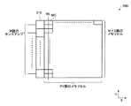
図4は、表示ドライバ20が実装された表示パネル10の一部を拡大する図である。表示領域12は複数の配線DQLによって表示ドライバ20の出力PAD700と接続されている。この配線はガラス基板に設けられた配線であっても良いし、フレキシブル基板等にて形成され、出力PAD700と表示領域12とを接続する配線であっても良い。
FIG. 4 is an enlarged view of a part of the
RAM200はそのY方向の長さがRYに設定されている。本実施形態では、この長さRYは、図3(A)のブロック幅ICYと同じに設定されているが、これに限定されない。例えば、長さRYはブロック幅ICY以下に設定されても良い。
In the
長さRYに設定されるRAM200には、複数のワード線WLと、複数のワード線WLを制御するワード線制御回路240が設けられている。また、RAM200には、複数のビット線BL、複数のメモリセルMC及びそれらを制御する制御回路(図示せず)が設けられている。RAM200のビット線BLはX方向に平行になるように設けられている。即ち、ビット線BLは表示領域12の一辺PL1に平行になるように設けられている。また、RAM200のワード線WLはY方向に平行になるように設けられている。即ち、ワード線WLは複数の配線DQLと平行になるように設けられている。
The
RAM200のメモリセルMCはワード線WLの制御により読み出しが行われ、その読み出されたデータがデータ線ドライバ100に供給される。即ち、ワード線WLが選択されると、Y方向に沿って配列された複数のメモリセルMCに格納されているデータがデータ線ドライバ100に供給されることになる。
The memory cell MC of the
図5は、図3(A)のA−A断面を示す断面図である。A−A断面はRAM200のメモリセルMCが配列されている領域の断面である。RAM200の形成される領域には、例えば5層の金属配線層が設けられている。図5では、例えば第1金属配線層ALA、その上層の第2金属配線層ALB、さらに上層の第3金属配線層ALC、第4金属配線層ALD、第5金属配線層ALEが示されている。第5金属配線層ALEには、例えば階調電圧発生回路500から階調電圧が供給される階調電圧用配線292が形成されている。また、第5金属配線層ALEには、電源回路600から供給される電圧や、外部から入出力PAD800を経由して供給される電圧等を供給するための電源用配線294が形成されている。本実施形態のRAM200は例えば第5金属配線層ALEを使用せずに形成できる。このため、前述のように第5金属配線層ALEに様々な配線を形成することができる。
FIG. 5 is a cross-sectional view showing the AA cross section of FIG. The AA section is a section of a region where the memory cells MC of the
また、第4金属配線層ALDにはシールド層290が形成されている。これにより、RAM200のメモリセルMCの上層の第5金属配線層ALEに様々な配線が形成されても、RAM200のメモリセルMCに与える影響を緩和することができる。なお、ワード線制御回路240等のRAM200の制御回路が形成されている領域の第4金属配線層ALDには、これらの回路の制御用の信号配線が形成されても良い。
A
第3金属配線層ALCに形成されている配線296は、例えばビット線BLや電圧VSS用配線に用いられる。また、第2金属配線層ALBに形成されている配線298は、例えばワード線WLや電圧VDD用配線として用いることができる。また、第1金属配線層ALAに形成されている配線299は、RAM200の半導体層に形成されている各ノードとの接続に用いることができる。
The
なお、上述の構成を変更して、第3金属配線層ALCにワード線用の配線を形成し、第2金属配線層ALBにビット線用の配線を形成するようにしても良い。 Alternatively, the above-described configuration may be changed so that a word line wiring is formed in the third metal wiring layer ALC and a bit line wiring is formed in the second metal wiring layer ALB.
以上のようにRAM200の第5金属配線層ALEに様々な配線を形成することができるので、図3(A)や図3(B)に示すように多種の回路ブロックをX方向に沿って配列することができる。
Since various wirings can be formed in the fifth metal wiring layer ALE of the
2.データ線ドライバ
2.1.データ線ドライバの構成
図6(A)は、データ線ドライバ100を示す図である。データ線ドライバ100は出力回路104、DAC120及びラッチ回路130を含む。DAC120はラッチ回路130にラッチされているデータに基づいて階調電圧を出力回路104に供給する。ラッチ回路130には、例えばRAM200から供給されたデータが格納される。例えば階調度がGビットに設定されている場合には、各ラッチ回路130にはGビットのデータが格納される。階調電圧は、階調度に応じて複数種類生成され、階調電圧発生回路500からデータ線ドライバ100に供給される。例えば、データ線ドライバ100に供給された複数の階調電圧は各DAC120に供給される。各DAC120はラッチ回路130にラッチされているGビットのデータに基づいて、階調電圧発生回路500から供給された複数種類の階調電圧から対応する階調電圧を選択し、出力回路104に出力する。
2. Data line driver 2.1. Configuration of Data Line Driver FIG. 6A shows the
出力回路104は、例えばオペアンプ(広義には演算増幅器)で構成されるが、これに限定されない。図6(B)に示すように出力回路104の代わりに出力回路102をデータ線ドライバ100に設けても良い。この場合、階調電圧発生回路500には複数のオペアンプが設けられている。
The output circuit 104 is composed of, for example, an operational amplifier (an operational amplifier in a broad sense), but is not limited to this. As shown in FIG. 6B, an output circuit 102 may be provided in the
図7はデータ線ドライバ100に設けられている複数のデータ線駆動セル110を示す図である。各データ線ドライバ100は複数のデータ線を駆動し、データ線駆動セル110は複数のデータ線のうちの1本を駆動する。例えば、データ線駆動セル110は、一ピクセルを構成するR用サブピクセル、G用サブピクセル及びB用サブピクセルのいずれか一つを駆動する。即ち、X方向のピクセル数PXが240の場合には、表示ドライバ20には、合計240×3=720個のデータ線駆動セル110が設けられていることになる。そして、この場合には各データ線ドライバ100には、例えば4BANK構成である場合、180個のデータ線駆動セル110が設けられている。
FIG. 7 is a diagram showing a plurality of data line driving
データ線駆動セル110は、例えば出力回路140、DAC120及びラッチ回路130を含むが、これに限定されない。例えば、出力回路140は外部に設けられても良い。なお、出力回路140は、図6(A)の出力回路104でも良いし、図6(B)の出力回路102でもよい。
The data
例えば、R用サブピクセル、G用サブピクセル及びB用サブピクセルのそれぞれの階調度を示す階調データがGビットに設定されている場合、RAM200からは、データ線駆動セル110にGビットのデータが供給される。ラッチ回路130は、Gビットのデータをラッチする。DAC120はラッチ回路130の出力に基づいて階調電圧を出力回路140を介して出力する。これにより、表示パネル10に設けられているデータ線を駆動することができる。
For example, when the gradation data indicating the gradation of each of the R subpixel, the G subpixel, and the B subpixel is set to G bits, the
2.2.一水平走査期間内の複数回読み出し
図8に本実施形態に係る比較例の表示ドライバ24を示す。この表示ドライバ24は、表示ドライバ24の一辺DLLが表示パネル10の表示領域12側の一辺PL1と対向するように実装される。表示ドライバ24には、Y方向の長さよりもX方向の長さの方が長く設定されているRAM205及びデータ線ドライバ105が設けられている。RAM205及びデータ線ドライバ105のX方向の長さは、表示パネル10のピクセル数PXが増加するに従って、長くなる。RAM205には複数のワード線WL及びビット線BLが設けられている。RAM205のワード線WLはX方向に沿って延在形成され、ビット線BLはY方向に沿って延在形成されている。即ち、ワード線WLはビット線BLよりも非常に長く形成される。また、ビット線BLはY方向に沿って延在形成されているため、表示パネル10のデータ線と平行であり、表示パネル10の一辺PL1と直交する。
2.2. Multiple readout within one horizontal scanning period FIG. 8 shows a
この表示ドライバ24は1H期間に1回だけワード線WLを選択する。そして、ワード線WLの選択によってRAM205から出力されるデータをデータ線ドライバ105がラッチし、複数のデータ線を駆動する。表示ドライバ24では、図8に示すようにワード線WLがビット線BLに比べて非常に長いため、データ線ドライバ100及びRAM205の形状がX方向に長くなり、表示ドライバ24に他の回路を配置するスペースを確保するのが難しい。そのため、表示ドライバ24のチップ面積の縮小を妨げる。また、その確保等に関する設計時間も無駄に要してしまうため、設計コスト削減を妨げる。
The
図8のRAM205は例えば図9(A)に示すようにレイアウトされる。図9(A)によると、RAM205は2分割され、そのうちの一つのX方向の長さは例えば「12」であるのに対し、Y方向の長さは「2」である。従って、RAM205の面積を「48」と示すことができる。これらの長さの値は、RAM205の大きさを示す上での比率の一例を示すものであり、実際の大きさを限定するものではない。なお、図9(A)〜図9(D)の符号241〜244はワード線制御回路を示し、符号206〜209はセンスアンプを示す。
The
これに対して、本実施形態では、RAM205を複数に分割し90度回転した状態でレイアウトすることができる。例えば、図9(B)に示すようにRAM205を4分割して90度回転した状態にレイアウトすることができる。4分割されたうちの一つであるRAM205−1は、センスアンプ207とワード線制御回路242を含む。また、RAM205−1のY方向の長さが「6」であり、X方向の長さが「2」である。よって、RAM205−1の面積は「12」となり、4ブロックの合計面積が「48」となる。しかしながら、表示ドライバ20のY方向の長さCYを短くしたいため、図9(B)の状態では都合が悪い。
On the other hand, in this embodiment, the
そこで、本実施形態では、図9(C)に示すように1H期間に複数回読み出しを行うことでRAM200のY方向の長さRYを短くすることができる。例えば、図9(C)では、1H期間に2回読み出しを行う場合を示す。この場合、1H期間にワード線WLを2回選択するため、例えばY方向に配列されたメモリセルMCの数を半分にすることができる。これにより、図9(C)に示すようにRAM200のY方向の長さを「3」とすることができる。その代わり、RAM200のX方向の長さは「4」となる。即ち、RAM200の合計の面積が「48」となり、図9(A)のRAM205とメモリセルMCが配列されている領域の面積が等しくなる。そして、これらのRAM200を図3(A)や図3(B)に示すように自由に配置することができるため、非常に柔軟にレイアウトが可能となり、効率的なレイアウトができる。
Therefore, in the present embodiment, the length RY in the Y direction of the
なお、図9(D)は、3回読み出しを行った場合の一例を示す。この場合、図9(B)のRAM205−1のY方向の長さ「6」を3分の1にすることができる。即ち、表示ドライバ20のY方向の長さCYをより短くしたい場合には、1H期間の読み出し回数を調整することで実現可能となる。
Note that FIG. 9D illustrates an example of a case where reading is performed three times. In this case, the length “6” in the Y direction of the RAM 205-1 in FIG. 9B can be reduced to one third. That is, when it is desired to shorten the length CY of the
上述のように本実施形態では、ブロック化されたRAM200を表示ドライバ20に設けることができる。本実施形態では、例えば4BANKのRAM200を表示ドライバ20に設けることができる。この場合、各RAM200に対応するデータ線ドライバ100−1〜100−4は図10に示すように対応するデータ線DLを駆動する。
As described above, in the present embodiment, the
具体的には、データ線ドライバ100−1はデータ線群DLS1を駆動し、データ線ドライバ100−2はデータ線群DLS2を駆動し、データ線ドライバ100−3はデータ線群DLS3を駆動し、データ線ドライバ100−4はデータ線群DLS4を駆動する。なお、各データ線群DLS1〜DLS4は、表示パネル10の表示領域12に設けられた複数のデータ線DLを例えば4ブロックに分割したうちの1ブロックである。このように4BANKのRAM200に対応して、4つのデータ線ドライバ100−1〜100−4を設け、それぞれに対応するデータ線を駆動させることで、表示パネル10の複数のデータ線を駆動することができる。
Specifically, the data line driver 100-1 drives the data line group DLS1, the data line driver 100-2 drives the data line group DLS2, the data line driver 100-3 drives the data line group DLS3, The data line driver 100-4 drives the data line group DLS4. Each of the data line groups DLS1 to DLS4 is one block among the plurality of data lines DL provided in the
2.3.データ線ドライバの分割構造
本実施形態では、図4のRAM200の長さRYを短くするために、一水平走査期間でのN回読み出し、例えば2回読み出しを前提として、データ線ドライバ100が、図11(A)に示すように第1のデータ線ドライバ100A(広義には第1の分割データ線ドライバ)及び第2のデータ線ドライバ100B(広義には第2の分割データ線ドライバ)と、N(2)分割されている。図11(A)に示すMは、1回のワード線選択によってRAM200から読み出されるデータのビット数である。
2.3. In this embodiment, in order to shorten the length RY of the
例えば、ピクセル数PXが240であり、ピクセルの階調度が18ビットであり、RAM200のBANK数が4BANKである場合、1H期間では、各RAM200から240×18÷4=1080ビットのデータがRAM200から出力されなければならない。
For example, when the pixel number PX is 240, the gradation of the pixel is 18 bits, and the BANK number of the
しかしながら、表示ドライバ100のチップ面積縮小のためには、RAM200の長さRYを短くしたい。そこで、図11(A)に示すように例えばデータ線ドライバ100A及び100BをX方向に分割する。そうすることで、Mを1080÷2=540に設定することができ、RAM200の長さRYをおよそ半分にすることができる。
However, in order to reduce the chip area of the
なお、データ線ドライバ100Aは表示パネル10のデータ線のうちの一部のデータ線を駆動する。また、データ線ドライバ100Bは、表示パネル10のデータ線のうち、データ線ドライバ100Aが駆動するデータ線以外のデータ線の一部を駆動する。このように、各データ線ドライバ100A,100Bは表示パネル10のデータ線をシェアして駆動する。
Note that the
具体的には、図11(B)に示すように1H期間に例えばワード線WL1及びWL2を選択する。即ち、1H期間に2回ワード線を選択する。そして、A1のタイミングでラッチ信号SLAを立ち下げる。このラッチ信号SLAは例えばデータ線ドライバ100Aに供給される。そして、データ線ドライバ100Aはラッチ信号SLAの例えば立ち下がりエッジに応じてRAM200から供給されるMビットのデータをラッチする。
Specifically, for example, word lines WL1 and WL2 are selected in the 1H period as shown in FIG. That is, the word line is selected twice in the 1H period. Then, the latch signal SLA falls at the timing of A1. The latch signal SLA is supplied to, for example, the
また、A2のタイミングでラッチ信号SLBを立ち下げる。このラッチ信号SLBは例えばデータ線ドライバ100Bに供給される。そして、データ線ドライバ100Bはラッチ信号SLBの例えば立ち下がりエッジに応じてRAM200から供給されるMビットのデータをラッチする。
Further, the latch signal SLB falls at the timing of A2. The latch signal SLB is supplied to, for example, the
さらに具体的には、図12に示すようにワード線WL1の選択によってM個のメモリセル群MCS1に格納されているデータがセンスアンプ回路210を介してデータ線ドライバ100A及び100Bに供給される。しかしながら、ワード線WL1の選択に対応してラッチ信号SLAが立ち下がるため、M個のメモリセル群MCS1に格納されているデータはデータ線ドライバ100Aにラッチされる。
More specifically, as shown in FIG. 12, the data stored in the M memory cell groups MCS1 is supplied to the
そして、ワード線WL2の選択によってM個のメモリセル群MCS2に格納されているデータがセンスアンプ回路210を介してデータ線ドライバ100A及び100Bに供給されるが、ワード線WL2の選択に対応してラッチ信号SLBが立ち下がる。このため、M個のメモリセル群MCS2に格納されているデータはデータ線ドライバ100Bにラッチされる。
Then, the data stored in the M memory cell groups MCS2 is supplied to the
このようにすると、Mを例えば540ビットに設定した場合、1H期間で2回読み出しを行うため、各データ線ドライバ100A、100Bには、M=540ビットのデータがラッチされることになる。即ち、合計1080ビットのデータがデータ線ドライバ100にラッチされることになり、前述の例で必要である1H期間に1080ビットを達成できる。そして、1H期間に必要なデータ量をラッチすることができ、且つ、RAM200の長さRYをおよそ半分に短くすることができる。これにより、表示ドライバ20のブロック幅ICYを短くすることができるので、表示ドライバ20の製造コスト削減が可能となる。
In this way, when M is set to 540 bits, for example, since data is read twice in the 1H period, data of M = 540 bits is latched in each of the
なお、図11(A)及び図11(B)では、一例として1H期間に2回の読み出しを行う例が図示されているが、これに限定されない。例えば、1H期間に4回読み出しを行うこともできるし、それ以上に設定することもできる。例えば4回読み出しの場合には、データ線ドライバ100を4段に分割することができ、さらにRAM200の長さRYを短くすることができる。この場合、前述を例に取れば、M=270に設定することができ、4段に分割されたデータ線ドライバのそれぞれに270ビットのデータがラッチされる。つまり、RAM200の長さRYをおよそ4分の1にしながら、1H期間に必要な1080ビットの供給を達成することができる。
Note that in FIGS. 11A and 11B, an example in which reading is performed twice in the 1H period is illustrated as an example; however, the present invention is not limited to this. For example, reading can be performed four times during the 1H period, or more than that can be set. For example, in the case of reading four times, the
また、図11(B)のA3及びA4に示すように、データ線イネーブル信号等(図示せず)による制御に基づいてデータ線ドライバ100A及び100Bの出力を立ち上げても良いし、A1及びA2に示すタイミングで、各データ線ドライバ100A、100Bがラッチした後にそのままデータ線に出力するようにしても良い。また、各データ線ドライバ100A、100Bにもう一段ラッチ回路を設けて、A1及びA2でラッチしたデータに基づく電圧を次の1H期間に出力するようにしても良い。こうすれば、1H期間に読み出しを行う回数を、画質劣化の心配なしに増やすことができる。
Further, as indicated by A3 and A4 in FIG. 11B, the outputs of the
なお、ピクセル数PYが320(表示パネル10の走査線が320本)であり、1秒間に60フレームの表示画行われる場合、1H期間は図11(B)に示すように約52μsecである。求め方としては、1sec÷60フレーム÷320≒52μsecである。これに対して、ワード線の選択は図11(B)に示すようにおよそ40nsecで行われる。つまり、1H期間に対して十分に短い期間に複数回のワード線選択(RAM200からのデータ読み出し)が行われるため、表示パネル10に対する画質の劣化に問題は生じない。
When the number of pixels PY is 320 (320 scanning lines of the display panel 10) and a display image of 60 frames is displayed per second, the 1H period is about 52 μsec as shown in FIG. 11B. The calculation method is 1 sec ÷ 60 frames ÷ 320≈52 μsec. On the other hand, the selection of the word line is performed in about 40 nsec as shown in FIG. That is, since word line selection (reading data from the RAM 200) is performed a plurality of times in a sufficiently short period with respect to the 1H period, there is no problem in image quality deterioration for the
また、Mの値は、次式で得ることができる。なお、BNKは、BANK数を示し、Nは1H期間に行われる読み出し回数を示し、Gは階調ビット数を示す。また、ピクセル数PX×3とは、表示パネル10のデータ線に対応する画素数(又は表示パネル10のデータ線の本数DLN)を意味する。 Further, the value of M can be obtained by the following equation. BNK indicates the number of BANKs, N indicates the number of readings performed during the 1H period, and G indicates the number of gradation bits. The number of pixels PX × 3 means the number of pixels corresponding to the data lines of the display panel 10 (or the number of data lines DLN of the display panel 10).
なお、本実施形態ではセンスアンプ回路210はラッチ機能を有するが、これに限定されない。例えばセンスアンプ回路210はラッチ機能を有さないものであっても良い。
In the present embodiment, the
2.4.データ線ドライバの細分割
図13は、1ピクセルを構成する各サブピクセルのうち、一例としてR用サブピクセルについてRAM200とデータ線ドライバ100の関係を説明するための図である。
2.4. Subdivision of Data Line Driver FIG. 13 is a diagram for explaining the relationship between the
例えば各サブピクセルの階調のGビットが64階調である6ビットに設定された場合、R用サブピクセルのデータ線駆動セル110A−R及び110B−Rには、6ビットのデータがRAM200から供給される。6ビットのデータを供給するために、RAM200のセンスアンプ回路210に含まれる複数のセンスアンプ211のうち例えば6つのセンスアンプ211が各データ線駆動セル110に対応する。
For example, when the G bit of each subpixel gradation is set to 6 bits, which is 64 gradations, 6-bit data is transferred from the
例えば、データ線駆動セル110A−RのY方向の長さSCYは、6つのセンスアンプ211のY方向の長さSAYに納める必要がある。同様に各データ線駆動セル110のY方向の長さは6つのセンスアンプ211の長さSAYに納める必要がある。長さSCYを6つのセンスアンプ211の長さSAYに納めることができない場合には、データ線ドライバ100のY方向の長さが、RAM200の長さRYよりも大きくなってしまい、レイアウト的に効率の悪い状態になってしまう。
For example, the length SCY in the Y direction of the data line driving
RAM200はプロセス的に微細化が進み、センスアンプ211のサイズも小さい。一方、図7に示すように、データ線駆動セル110には複数の回路が設けられている。特に、DAC120やラッチ回路130は回路サイズが大きくなり、小さく設計することが難しい。さらに、DAC120やラッチ回路130は入力されるビット数が増えると大きくなる。つまり、長さSCYを6つのセンスアンプ211のトータル長さSAYに納めることが困難である場合がある。
The
これに対して、本実施形態では、1H内読み出し回数Nで分割されたデータ線ドライバ100A,100Bをさらにk(kは2以上の整数)分割し、X方向にスタックすることができる。図14は、1H期間にN=2回読み出しを行うように設定されたRAM200において、データ線ドライバ100A及び100Bがそれぞれk=2分割されてスタックされた構成例を示す。なお、図14では、2回読み出しに設定されたRAM200についての構成例であり、これに限定されない。例えばN=4回読み出しに設定されている場合には、データ線ドライバはX方向において4×2=8段に分割される。
On the other hand, in this embodiment, the
図13の各データ線ドライバ100A、100Bは、図14に示すように、それぞれが、データ線ドライバ100A1及び100A2、データ線ドライバ100B1及び100B2に分割されている。そして、データ線駆動セル110A1−R等はそのY方向の長さがSCY2に設定されている。長さSCY2は、図14によるとセンスアンプ211がG×2個配列された場合のY方向の長さSAY2に収まるように設定されている。つまり、各データ線駆動セル110を形成する際に、図13に比べてY方向に許容される長さが拡大され、レイアウト的に効率の良い設計が可能である。
As shown in FIG. 14, each of the
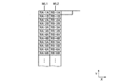
次に図14における構成の動作を説明する。例えばワード線WL1が選択されると、各センスアンプブロック210−1、210−2、210−3、210−4等を介して計Mビットのデータがデータ線ドライバ100A1、100A2、100B1、100B2の少なくともいずれかに供給される。このとき、例えば、センスアンプブロック210−1から出力されるGビットのデータは、例えばデータ線駆動セル110A1−R及び110B1−Rに供給される。そして、センスアンプブロック210−2から出力されるGビットのデータは、例えばデータ線駆動セル110A2−R及び110B2−Rに供給される。 Next, the operation of the configuration in FIG. 14 will be described. For example, when the word line WL1 is selected, a total of M bits of data are transferred to the data line drivers 100A1, 100A2, 100B1, and 100B2 through the sense amplifier blocks 210-1, 210-2, 210-3, and 210-4. Supplied to at least one of them. At this time, for example, the G-bit data output from the sense amplifier block 210-1 is supplied to, for example, the data line driving cells 110A1-R and 110B1-R. The G-bit data output from the sense amplifier block 210-2 is supplied to, for example, the data line driving cells 110A2-R and 110B2-R.
このとき、図11(B)に示すタイミングチャートと同様に、ワード線WL1が選択されたときに対応してラッチ信号SLA(広義には第1のラッチ信号)が立ち下がる。そして、このラッチ信号SLAはデータ線駆動セル110A1−Rを含むデータ線ドライバ100A1及びデータ線駆動セル110A2−Rを含むデータ線ドライバ100A2に供給される。従って、ワード線WL1の選択によってセンスアンプブロック210−1から出力されるGビットのデータ(メモリセル群MCS11に格納されているデータ)はデータ線駆動セル110A1−Rにラッチされる。同様に、ワード線WL1の選択によってセンスアンプブロック210−2から出力されるGビットのデータ(メモリセル群MCS12に格納されているデータ)はデータ線駆動セル110A2−Rにラッチされる。 At this time, similarly to the timing chart shown in FIG. 11B, the latch signal SLA (first latch signal in a broad sense) falls in response to the selection of the word line WL1. The latch signal SLA is supplied to the data line driver 100A1 including the data line driving cell 110A1-R and the data line driver 100A2 including the data line driving cell 110A2-R. Accordingly, G-bit data (data stored in the memory cell group MCS11) output from the sense amplifier block 210-1 by the selection of the word line WL1 is latched in the data line driving cell 110A1-R. Similarly, G-bit data (data stored in the memory cell group MCS12) output from the sense amplifier block 210-2 by the selection of the word line WL1 is latched in the data line driving cell 110A2-R.
センスアンプブロック210−3、210−4についても上記と同様であり、データ線駆動セル110A1−Gにはメモリセル群MCS13に格納されているデータがラッチされ、データ線駆動セル110A2−Gにはメモリセル群MCS14に格納されているデータがラッチされる。 The sense amplifier blocks 210-3 and 210-4 are similar to the above, and the data stored in the memory cell group MCS13 is latched in the data line driving cell 110A1-G, and the data line driving cell 110A2-G has Data stored in the memory cell group MCS14 is latched.
また、ワード線WL2が選択される場合は、ワード線WL2の選択に対応してラッチ信号SLBが(広義には第Nのラッチ信号)立ち下がる。そして、このラッチ信号SLBはデータ線駆動セル110B1−Rを含むデータ線ドライバ100B1及びデータ線駆動セル110B2−Rを含むデータ線ドライバ100B2に供給される。従って、ワード線WL2の選択によってセンスアンプブロック210−1から出力されるGビットのデータ(メモリセル群MCS21に格納されているデータ)はデータ線駆動セル110B1−Rにラッチされる。同様に、ワード線WL2の選択によってセンスアンプブロック210−2から出力されるGビットのデータ(メモリセル群MCS22に格納されているデータ)はデータ線駆動セル110B2−Rにラッチされる。 In addition, when the word line WL2 is selected, the latch signal SLB (Nth latch signal in a broad sense) falls corresponding to the selection of the word line WL2. The latch signal SLB is supplied to the data line driver 100B1 including the data line driving cell 110B1-R and the data line driver 100B2 including the data line driving cell 110B2-R. Therefore, G-bit data (data stored in the memory cell group MCS21) output from the sense amplifier block 210-1 by the selection of the word line WL2 is latched in the data line driving cell 110B1-R. Similarly, G-bit data (data stored in the memory cell group MCS22) output from the sense amplifier block 210-2 by the selection of the word line WL2 is latched in the data line driving cell 110B2-R.
ワード線WL2の選択においても、センスアンプブロック210−3、210−4については上記と同様であり、データ線駆動セル110B1−Gにはメモリセル群MCS23に格納されているデータがラッチされ、データ線駆動セル110B2−Gにはメモリセル群MCS24に格納されているデータがラッチされる。 In the selection of the word line WL2, the sense amplifier blocks 210-3 and 210-4 are the same as described above, and the data stored in the memory cell group MCS23 is latched in the data line driving cell 110B1-G, and the data The data stored in the memory cell group MCS24 is latched in the line drive cell 110B2-G.
このようにデータ線ドライバ100A、100Bが分割された場合において、RAM200に格納されるデータを図15(B)に示す。図15(B)に示すようにRAM200には、Y方向に沿ってR用サブピクセルデータ、R用サブピクセルデータ、G用サブピクセルデータ、G用サブピクセルデータ、B用サブピクセルデータ、B用サブピクセルデータ・・・という順番でデータが格納される。一方、図13のような構成の場合には、図15(A)に示すようにRAM200には、Y方向に沿ってR用サブピクセルデータ、G用サブピクセルデータ、B用サブピクセルデータ、R用サブピクセルデータ・・・という順番でデータが格納される。
FIG. 15B shows data stored in the
なお、図13では長さSAYは6つのセンスアンプ211に示されているが、これに限定されない。例えば、階調度が8ビットの場合には長さSAYは8つのセンスアンプ211の長さに相当する。
In FIG. 13, the length SAY is shown for the six
また、図14では一例として各データ線ドライバ100A、100Bをそれぞれk=2分割する構成が示されているが、これに限定されない。例えば3分割でも良いし、4分割でも良い。そして、例えばデータ線ドライバ100Aを3分割した場合、3分割されたものに同じラッチ信号SLAを供給するようにすればよい。また、1H読み出し回数と等しい分割数kの変形例として、k=3分割した場合には、それぞれをR用サブピクセルデータ、G用サブピクセルデータ、B用サブピクセルデータのドライバとすることができる。その構成を図16に示す。図16では、3つに分割されたデータ線ドライバ101A1、101A2、101A3が示されている。データ線ドライバ101A1は、データ線駆動セル111A1を含み、データ線ドライバ101A2は、データ線駆動セル111A2を含み、データ線ドライバ101A3は、データ線駆動セル111A3を含む。
FIG. 14 shows a configuration in which each
そして、ワード線WL1の選択に対応してラッチ信号SLAが立ち下がる。前述と同様にラッチ信号SLAは、各データ線ドライバ101A1、101A2、101A3に供給される。 Then, the latch signal SLA falls corresponding to the selection of the word line WL1. As described above, the latch signal SLA is supplied to each of the data line drivers 101A1, 101A2, and 101A3.
このようにすると、ワード線WL1の選択によって、メモリセル群MCS11に格納されているデータが例えばR用サブピクセルデータとしてデータ線駆動セル111A1に格納される。同様にメモリセル群MCS12に格納されているデータが例えばG用サブピクセルデータとしてデータ線駆動セル111A2に格納され、メモリセル群MCS13に格納されているデータが例えばB用サブピクセルデータとしてデータ線駆動セル111A3に格納される。 In this way, the data stored in the memory cell group MCS11 is stored in the data line driving cell 111A1 as, for example, R subpixel data by selecting the word line WL1. Similarly, data stored in the memory cell group MCS12 is stored in the data line driving cell 111A2, for example, as G subpixel data, and data stored in the memory cell group MCS13 is, for example, data line driving as the B subpixel data. Stored in cell 111A3.
従って、図15(A)のようにRAM200に書き込まれるデータをY方向でR用サブピクセルデータ、G用サブピクセルデータ、B用サブピクセルデータという順番に配列することができる。この場合も、各データ線ドライバ101A1、101A2、101A3をさらにk分割することができる。
Therefore, as shown in FIG. 15A, the data written in the
3.RAM
3.1.メモリセルの構成
各メモリセルMCは例えばSRAM(Static-Random-Access-Memory)で構成することができる。図17(A)にメモリセルMCの回路の一例を示す。また、図17(B)にメモリセルMCのレイアウトの一例を示す。
3. RAM
3.1. Configuration of Memory Cell Each memory cell MC can be configured by, for example, SRAM (Static-Random-Access-Memory). FIG. 17A shows an example of a circuit of the memory cell MC. FIG. 17B shows an example of the layout of the memory cell MC.
図17(B)に示すように、メモリセルMCはメインワード線MWLとサブワード線SWLを含み、これらは方向DR1(広義には、メモリセルの短辺の延びる方向)に沿って延在形成されている。また、メモリセルMCはビット線BL及びビット線/BLを含み、これらは、方向DR2(広義には、メモリセルの長辺の延びる方向)に沿って延在形成されている。本実施形態では、メモリセルMCは例えば5層の金属配線を用いて形成される。そして、ビット線BL、/BLは例えば第3層の金属配線層に形成され、その下層の第2層の金属配線層にメインワード線MWLが形成される。サブワード線SWLは例えばポリシリコン等の導電体で形成される。 As shown in FIG. 17B, the memory cell MC includes a main word line MWL and a sub word line SWL, which are formed to extend along the direction DR1 (in a broad sense, the direction in which the short side of the memory cell extends). ing. The memory cell MC includes a bit line BL and a bit line / BL, which are formed to extend along the direction DR2 (in a broad sense, the direction in which the long side of the memory cell extends). In the present embodiment, the memory cell MC is formed using, for example, five layers of metal wiring. For example, the bit lines BL and / BL are formed in the third metal wiring layer, and the main word line MWL is formed in the second metal wiring layer below the bit lines. The sub word line SWL is formed of a conductor such as polysilicon.
メモリセルMCのサイズにおいて、ビット線BL、/BLに沿った長さMCX(広義にはメモリセルの長辺)は、メインワード線MWL又はサブワード線SWLに沿った長さMCY(広義にはメモリセルの短辺)に比べて十分に長い。本実施形態では、このようなレイアウトのメモリセルMCをRAM200に用いることができるが、これに限定されない。例えば、メモリセルMCは、長さMCXよりも長さMCYが長く設定されてもよい。
In the size of the memory cell MC, the length MCX along the bit lines BL and / BL (the long side of the memory cell in a broad sense) is the length MCY along the main word line MWL or the sub word line SWL (the memory in a broad sense). Long enough compared to the short side of the cell). In the present embodiment, the memory cells MC having such a layout can be used for the
なお、本実施形態では、メインワード線MWL及びサブワード線SWLが所定の複数の箇所で電気的に接続されている。これにより、サブワード線SWLを金属配線であるメインワード線MWLを用いて低抵抗化することができる。また、本実施形態では、メインワード線MWL及びサブワード線SWLを1本のワード線WLとみなすことができる。 In this embodiment, the main word line MWL and the sub word line SWL are electrically connected at a plurality of predetermined locations. Thereby, the resistance of the sub word line SWL can be reduced by using the main word line MWL which is a metal wiring. In the present embodiment, the main word line MWL and the sub word line SWL can be regarded as one word line WL.
3.2.センスアンプの共用
図18(A)に示すようにセンスアンプ211のY方向の長さSAY3は、メモリセルMCの長さMCYよりも十分に大きい。このため、ワード線WLを選択する際に、一つのセンスアンプ211に対して一つのメモリセルMCを対応させるレイアウトは、効率が悪い。
3.2. Sharing of Sense Amplifier As shown in FIG. 18A, the length SAY3 of the
これに対して、本実施形態では、このようなメモリセルMCであっても効率的にレイアウト配置可能にすることができる。図18(B)に示すように、ワード線WLの選択において、一つのセンスアンプ211に対して複数(例えば2つ)のメモリセルMCを対応させる。これにより、センスアンプ211の長さSAY3とメモリセルMCの長さMCYの差を問題とせずに、効率的にメモリセルMCをRAM200に配列することができる。
On the other hand, in this embodiment, even such a memory cell MC can be efficiently laid out. As shown in FIG. 18B, in selecting the word line WL, a plurality of (for example, two) memory cells MC are associated with one
図18(B)によると、選択型センスアンプSSAは、センスアンプ211と、スイッチ回路220と、スイッチ回路230を含む。選択型センスアンプSSAには、ビット線対BL、/BLが例えば2組接続されている。
According to FIG. 18B, the selective sense amplifier SSA includes a
スイッチ回路220は、選択信号COLA(広義にはセンスアンプ用選択信号)に基づいて、一方の組のビット線対BL、/BLをセンスアンプ211に接続する。同様にスイッチ回路230は、選択信号COLBに基づいて、他方の組のビット線対BL、/BLをセンスアンプ211に接続する。なお、選択信号COLA、COLBは、例えばその信号レベルが排他的に制御される。具体的には、選択信号COLAがスイッチ回路220をアクティブに設定する信号に設定された場合には、選択信号COLBはスイッチ回路230をノンアクティブに設定する信号に設定される。即ち、選択型センスアンプSSAは例えば2組のビット線対BL、/BLによって供給される2ビット(広義にはNビット又はLビット)のデータのうちのいずれか1ビットのデータを選択して対応するデータを出力する。
The
図19に選択型センスアンプSSAが設けられたRAM200を示す。図19では、一例として、1H期間に2回(広義にはN回)読み出しを行う場合であり、例えば階調度のGビットが6ビットである場合の構成が示されている。このような場合、RAM200には、図20に示すようにM個の選択型センスアンプSSAが設けられる。従って、1回のワード線WLの選択によってデータ線ドライバ100に供給されるデータは計Mビットである。これに対して、図20のRAM200にはメモリセルMCがY方向においてM×2(広義にはM×L)個配列されている。そして、X方向では、ピクセル数PYと同じ個数のメモリセルMCが配列されている。例えば図13に示すような場合であって、1H期間に2回読み出しが行われる場合には、RAM200のX方向に配列されるメモリセルMCの数は、ピクセル数PY×読み出し回数(2回)である。これに対して、図20のRAM200では、選択型センスアンプSSAに2組のビット線対BL、/BLが接続されているため、RAM200のX方向に配列されるメモリセルMCの数はピクセル数PYと同じ個数でよい。
FIG. 19 shows a
図20では、1H期間の読み出し回数Nが2であり、Y方向に配列されているメモリセルMCの数がM×2個であるが、これに限定されない。例えば、RAM200には、Y方向にM×L個のメモリセルが配列されても良い。この場合、RAM200のX方向に配列されるメモリセルMCの数は、表示パネル10の走査線の本数をSCN本とすると、1H期間の読み出し回数N×走査線の本数SCN/Lで求めることができる。このような構成の場合、センスアンプ回路210には、M×Lビットのデータが1回のワード線WLの選択により供給される。そして、センスアンプ回路210はM×LビットのデータのうちのMビットのデータをデータ線ドライバ100に出力する。
In FIG. 20, the number of readings N in the 1H period is 2, and the number of memory cells MC arranged in the Y direction is M × 2. However, the present invention is not limited to this. For example, in the
これにより、メモリセルMCの長さMCXが長さMCYより長い場合であっても、RAM200のX方向のサイズが大きくならないようにすることができる。
Thereby, even if the length MCX of the memory cell MC is longer than the length MCY, the size of the
3.3.動作
次に図19に示すRAM200の動作を説明する。本実施形態では、1H期間にワード線の選択をN回行うことができる。そして、そのバリエーションはいくつかあり、N回の選択のうちのL(L≦N)回を同一のワード線に対して行う方法と、N回の選択を異なるN本のワード線に割り当てる方法が挙げられる。
3.3. Operation Next, the operation of the
まずその一つの方法である前者の一例としてN=Lである場合を図21(A)、図21(B)のタイミングチャートを用いて説明する。 First, as an example of the former which is one method, a case where N = L will be described with reference to timing charts of FIGS. 21A and 21B.
図21(A)のB1に示すタイミングで選択信号COLAがアクティブに設定され、B2に示すタイミングでワード線WL1が選択される。このとき、選択信号COLAがアクティブであるため、選択型センスアンプSSAはA側のメモリセルMC、つまりメモリセルMC−1Aのデータを検出して出力する。そして、B3のタイミングでラッチ信号SLAが立ち下がると、データ線駆動セル110A−Rは、メモリセルMC−1Aに格納されているデータをラッチする。
The selection signal COLA is set active at the timing indicated by B1 in FIG. 21A, and the word line WL1 is selected at the timing indicated by B2. At this time, since the selection signal COLA is active, the selective sense amplifier SSA detects and outputs data of the A-side memory cell MC, that is, the memory cell MC-1A. When the latch signal SLA falls at the timing of B3, the data
また、B4のタイミングで選択信号COLBがアクティブに設定され、B5に示すタイミングでワード線WL1が選択される。このとき、選択信号COLBがアクティブであるため、選択型センスアンプSSAはB側のメモリセルMC、つまりメモリセルMC−1Bのデータを検出して出力する。そして、B6のタイミングでラッチ信号SLBが立ち下がると、データ線駆動セル110B−Rは、メモリセルMC−1Bに格納されているデータをラッチする。なお、図21(A)では、2回読み出しのうち、2回ともワード線WL1が選択される。
Further, the selection signal COLB is set to active at the timing of B4, and the word line WL1 is selected at the timing of B5. At this time, since the selection signal COLB is active, the selective sense amplifier SSA detects and outputs data of the memory cell MC on the B side, that is, the memory cell MC-1B. When the latch signal SLB falls at the timing of B6, the data
これにより、1H期間の2回読み出しによるデータ線ドライバ100のデータラッチが完了する。
Thereby, the data latch of the
また、図21(B)には、ワード線WL2が選択される場合のタイミングチャートが示されている。動作は上記と同様であり、その結果、ワード線WL2がB7やB8に示すように選択される場合には、メモリセルMC−2Aのデータがデータ線駆動セル110A−Rにラッチされ、メモリセルMC−2Bのデータがデータ線駆動セル110B−Rにラッチされる。
FIG. 21B shows a timing chart when the word line WL2 is selected. The operation is the same as described above. As a result, when the word line WL2 is selected as indicated by B7 or B8, the data in the memory cell MC-2A is latched in the data
これにより、図21(A)の1H期間とは異なる1H期間での2回読み出しによるデータ線ドライバ100のデータラッチが完了する。
As a result, the data latch of the
このような読み出し方法に対して、RAM200の各メモリセルMCには、図22に示すようにデータが格納される。例えば、データRA−1〜RA−6はデータ線駆動セル110A−Rに供給するためのR画素の6ビットのデータであり、データRB−1〜RB−6はデータ線駆動セル110B−Rに供給するためのR画素の6ビットのデータである。
For such a reading method, data is stored in each memory cell MC of the
図22に示すように、例えばワード線WL1に対応するメモリセルMCには、Y方向に沿って、データRA−1(データ線ドライバ100Aがラッチするためのデータ)、RB−1(データ線ドライバ100Bがラッチするためのデータ)、RA−2(データ線ドライバ100Aがラッチするためのデータ)、RB−2(データ線ドライバ100Bがラッチするためのデータ)、RA−3(データ線ドライバ100Aがラッチするためのデータ)、RB−3(データ線ドライバ100Bがラッチするためのデータ)・・という順番で格納される。即ち、RAM200には、Y方向に沿って(データ線ドライバ100Aがラッチするためのデータ)と(データ線ドライバ100Bがラッチするためのデータ)が交互に格納される。
As shown in FIG. 22, for example, in the memory cell MC corresponding to the word line WL1, along the Y direction, data RA-1 (data to be latched by the
なお、図21(A)、図21(B)に示す読み出し方法は、1H期間に2回読み出しを行うが、1H期間に同一のワード線WLが選択される。 Note that the reading method illustrated in FIGS. 21A and 21B performs reading twice in the 1H period, but the same word line WL is selected in the 1H period.
上記には、1回のワード線の選択において選択されるメモリセルMCのうち、各選択型センスアンプSSAは2個のメモリセルMCからデータを受ける内容が開示されているが、これに限定されない。例えば、1回のワード線の選択において選択されるメモリセルMCのうち、各選択型センスアンプSSAがN個のメモリセルMCからNビットのデータを受けるような構成でも良い。その場合には、選択型センスアンプSSAは、同一のワード線の1回目の選択の際には、第1〜第NのメモリセルMCのN個のメモリセルMCのうち、第1のメモリセルMCから受ける1ビットのデータを選択する。また、選択型センスアンプSSAはK(1≦K≦N)回目のワード線の選択の際には、第KのメモリセルMCから受ける1ビットのデータを選択する。 Although the above description discloses that each of the selectable sense amplifiers SSA receives data from two memory cells MC among the memory cells MC selected in one word line selection, the present invention is not limited to this. . For example, among the memory cells MC selected in one word line selection, each selective sense amplifier SSA may receive N bits of data from N memory cells MC. In this case, the selection type sense amplifier SSA selects the first memory cell among the N memory cells MC of the first to Nth memory cells MC when selecting the same word line for the first time. Select 1-bit data received from MC. In addition, the selection type sense amplifier SSA selects 1-bit data received from the Kth memory cell MC in the K (1 ≦ K ≦ N) word line selection.
図18(A)及び図18(B)の変形例としてL<Nである場合は、1H期間にL回選択される同一のワード線WLを(N/L)本選択し、1H期間にRAM200よりデータが読み出される回数が(N/L×L=N)回とすることができる。例えば、N=4、L=2とすると、図18(A)及び図18(B)に示す4回のワード線選択が同一水平走査期間1H内に実施される。すなわち、1H期間内にワード線WL1を2回、ワード線WL2を2回選択することで、N=4回読出しする方法である。
As a modification of FIGS. 18A and 18B, when L <N, the same word line WL selected L times in the 1H period is selected (N / L), and the
また、L<Lである場合には、1H期間に同一のワード線をL回選択し、残りの回数である(N−L)回を異なるワード線の選択に割り当てる方法でも良い。例えば、N=4、L=2とした場合、1H期間に同一のワード線を2回選択し、異なる2本ワード線を1回ずつ選択するようにしてもよい。また、N=6、L=2とした場合に、1H期間に異なる2本のワード線を2回ずつ選択し、さらに異なる2本のワード線をそれぞれ1回ずつ選択して計6回の選択を行うようにしても良い。 When L <L, the same word line may be selected L times in the 1H period, and the remaining number (N−L) times may be assigned to selection of different word lines. For example, when N = 4 and L = 2, the same word line may be selected twice during the 1H period, and two different word lines may be selected once. In addition, when N = 6 and L = 2, two different word lines are selected twice in the 1H period, and two different word lines are selected once each for a total of six selections. May be performed.
次に後者の制御方法を図23(A)及び図23(B)を用いて説明する。この場合、1H期間に2本(N本)の異なるワード線が選択される。また、一垂直走査期間において同一のワード線が2回(L回)選択される。 Next, the latter control method will be described with reference to FIGS. 23 (A) and 23 (B). In this case, two (N) different word lines are selected in the 1H period. Further, the same word line is selected twice (L times) in one vertical scanning period.
図23(A)のC1に示すタイミングで選択信号COLAがアクティブに設定され、C2に示すタイミングでワード線WL1が選択される。これにより図19のメモリセルMC−1A及びMC−1Bが選択される。このとき、選択信号COLAがアクティブであるため、選択型センスアンプSSAはA側のメモリセルMC(広義には第1のメモリセル)、つまりメモリセルMC−1Aのデータを検出して出力する。そして、C3のタイミングでラッチ信号SLAが立ち下がると、データ線駆動セル110A−Rは、メモリセルMC−1Aに格納されているデータをラッチする。
The selection signal COLA is set active at the timing indicated by C1 in FIG. 23A, and the word line WL1 is selected at the timing indicated by C2. As a result, the memory cells MC-1A and MC-1B of FIG. 19 are selected. At this time, since the selection signal COLA is active, the selective sense amplifier SSA detects and outputs data of the A side memory cell MC (first memory cell in a broad sense), that is, the memory cell MC-1A. When the latch signal SLA falls at the timing of C3, the data
また、C4に示すタイミングでワード線WL2が選択され、メモリセルMC−2A及びMC−2Bが選択される。このとき、選択信号COLAはアクティブであるため、選択型センスアンプSSAはA側のメモリセルMC、つまりメモリセルMC−2Aのデータを検出して出力する。そして、C5のタイミングでラッチ信号SLBが立ち下がると、データ線駆動セル110B−Rは、メモリセルMC−2Aに格納されているデータをラッチする。
Further, the word line WL2 is selected at the timing indicated by C4, and the memory cells MC-2A and MC-2B are selected. At this time, since the selection signal COLA is active, the selection type sense amplifier SSA detects and outputs data of the A-side memory cell MC, that is, the memory cell MC-2A. When the latch signal SLB falls at the timing of C5, the data
これにより、1H期間の2回読み出しによるデータ線ドライバ100のデータラッチが完了する。
Thereby, the data latch of the
また、図23(A)で示される1H期間とは異なる1H期間での読み出しを図23(B)を用いて説明する。図23(B)のC6に示すタイミングで選択信号COLBがアクティブに設定され、C7に示すタイミングでワード線WL1が選択される。これにより図19のメモリセルMC−1A及びMC−1Bが選択される。このとき、選択信号COLBがアクティブであるため、選択型センスアンプSSAはB側のメモリセルMC(広義には第1〜第Nのメモリセルのうちの第1のメモリセルと異なるメモリセル)、つまりメモリセルMC−1Bのデータを検出して出力する。そして、C8のタイミングでラッチ信号SLAが立ち下がると、データ線駆動セル110A−Rは、メモリセルMC−1Bに格納されているデータをラッチする。
Further, reading in a 1H period different from the 1H period shown in FIG. 23A will be described with reference to FIG. The selection signal COLB is set active at the timing indicated by C6 in FIG. 23B, and the word line WL1 is selected at the timing indicated by C7. As a result, the memory cells MC-1A and MC-1B of FIG. 19 are selected. At this time, since the selection signal COLB is active, the selective sense amplifier SSA has a memory cell MC on the B side (in a broad sense, a memory cell different from the first memory cell among the first to Nth memory cells), That is, the data of the memory cell MC-1B is detected and output. When the latch signal SLA falls at the timing C8, the data
また、C9に示すタイミングでワード線WL2が選択され、メモリセルMC−2A及びMC−2Bが選択される。このとき、選択信号COLBはアクティブであるため、選択型センスアンプSSAはB側のメモリセルMC、つまりメモリセルMC−2Bのデータを検出して出力する。そして、C10のタイミングでラッチ信号SLBが立ち下がると、データ線駆動セル110B−Rは、メモリセルMC−2Bに格納されているデータをラッチする。
Further, the word line WL2 is selected at the timing indicated by C9, and the memory cells MC-2A and MC-2B are selected. At this time, since the selection signal COLB is active, the selection type sense amplifier SSA detects and outputs data of the B-side memory cell MC, that is, the memory cell MC-2B. When the latch signal SLB falls at the timing of C10, the data
これにより、図23(A)の1H期間とは異なる1H期間での2回読み出しによるデータ線ドライバ100のデータラッチが完了する。
Thus, the data latch of the
このような読み出し方法に対して、RAM200の各メモリセルMCには、図24に示すようにデータが格納される。例えば、データRA−1A〜RA−6A及びデータRA−1B〜RA−6Bはデータ線駆動セル110A−Rに供給するためのR用サブピクセルのための6ビットのデータである。データRA−1A〜RA−6Aは図23(A)に示す1H期間におけるR用サブピクセルデータであり、データRA−1B〜RA−6Bは図23(B)に示す1H期間におけるR用サブピクセルデータである。
For such a reading method, data is stored in each memory cell MC of the
また、データRB−1A〜RB−6A及びデータRB−1B〜RB−6Bはデータ線駆動セル110B−Rに供給するためのR用サブピクセルのための6ビットのデータである。データRB−1A〜RB−6Aは図23(A)に示す1H期間におけるR用サブピクセルデータであり、データRB−1B〜RB−6Bは図23(B)に示す1H期間におけるR用サブピクセルデータである。
Data RB-1A to RB-6A and data RB-1B to RB-6B are 6-bit data for R subpixels to be supplied to the data
図24に示すように、RAM200には、X方向に沿ってデータRA−1A(データ線ドライバ100Aがラッチするためのデータ)、RB−1A(データ線ドライバ100Bがラッチするためのデータ)という順番に各メモリセルMCに格納される。
As shown in FIG. 24, the
また、RAM200には、Y方向に沿って、データRA−1A(図23(A)の1H期間にデータ線ドライバ100Aがラッチするためのデータ)、データRA−1B(図23(A)の1H期間にデータ線ドライバ100Aがラッチするためのデータ)、データRA−2A(図23(A)の1H期間にデータ線ドライバ100Aがラッチするためのデータ)、データRA−2B(図23(A)の1H期間にデータ線ドライバ100Aがラッチするためのデータ)・・という順番で格納される。即ち、RAM200には、Y方向に沿って、ある1H期間にデータ線ドライバ100Aにラッチされるデータと、その1H期間とは異なる他の1H期間にデータ線ドライバ100Aにラッチされるデータとが、交互に格納される。
Further, in the
なお図23(A)、図23(B)に示す読み出し方法は、1H期間に2回読み出しを行うが、1H期間に異なるワード線WLが選択される。そして、1垂直期間(つまり、1フレーム期間)に同一のワード線が2回選択される。これは、選択型センスアンプSSAが2組のビット線対BL、/BLを接続するからである。従って、選択型センスアンプSSAに3組又はそれ以上のビット線BL、/BLが接続される場合には、1垂直期間に同一のワード線が3回又はそれ以上の回数だけ選択されることになる。 Note that the reading method illustrated in FIGS. 23A and 23B performs reading twice in the 1H period, but different word lines WL are selected in the 1H period. The same word line is selected twice in one vertical period (that is, one frame period). This is because the selective sense amplifier SSA connects two pairs of bit lines BL and / BL. Accordingly, when three or more sets of bit lines BL and / BL are connected to the selective sense amplifier SSA, the same word line is selected three times or more in one vertical period. Become.
なお、本実施形態では、上述されたワード線WLの制御は、例えば図4のワード線制御回路240によって制御される。
In the present embodiment, the above-described control of the word line WL is controlled by, for example, the word
3.4.ワード線制御回路の配置
本実施形態では、RAM200のY方向に沿って配列されたメモリセルの数がM×2個である場合、図25に示すようにローデコーダ(広義にはワード線制御回路)242をY方向において、およそ真ん中に設けることができる。
3.4. Arrangement of Word Line Control Circuit In this embodiment, when the number of memory cells arranged in the Y direction of the
図25に示すように、RAM200A及び200Bの各々には、Y方向に沿ってそれぞれ、例えばM個のメモリセルMCが配列されている。そして、ローデコーダ242は、CPU/LCD制御回路250からの信号に基づいて、RAM200A及び200Bのワード線WLを制御する。CPU/LCD制御回路250は例えば外部のホストの制御に基づいて、ローデコーダ242、出力回路260A、260B、CPUライト/リード回路280A、280B、カラムデコーダ270A及び270Bを制御する。
As shown in FIG. 25, for example, M memory cells MC are arranged in each of the
CPUライト/リード回路280A、280BはCPU/LCD制御回路250からの信号に基づいて、ホスト側からのデータをRAM200に書き込んだり、RAM200に格納されているデータを読み出して例えばホスト側に出力する制御を行ったりする。カラムデコーダ270A、270Bは、CPU/LCD制御回路250からの信号に基づいて、RAM200のビット線BL、/BLの選択制御を行う。
The CPU write /
また、各RAM200A及び200BのY方向に沿って配列されるメモリセルMCの数はMに限定されない。例えば、RAM200Aには、Y方向に沿ってM−α(αは任意の正の整数)個のメモリセルMCが配列され、RAM200BにはY方向に沿ってM+α個のメモリセルMCが配列されても良い。またはその逆でも良い。
Further, the number of memory cells MC arranged along the Y direction of each of the
なお、出力回路260A、260Bは、例えば複数の選択型センスアンプSSAを含み、例えばワード線WL1A、WL1Bの選択によって各RAM200A、200Bから出力されるデータの合計Mビットのデータをデータ線ドライバ100に出力する。
The
本実施形態では、選択型センスアンプSSAに例えば2組のビット線対BL、/BLが接続される場合、図20に示すようにRAM200には、Y方向に沿ってM×2個のメモリセルが配列されることになる。このような場合、1ワード線WLに接続されるメモリセルMCの数がM×2個となり、1ワード線WLに寄生する容量が増える。その結果、ワード線制御回路によるワード線選択に必要な消費電力が増大し、低消費電力化の妨げとなる。また、寄生容量に起因して、ワード線に選択電圧が供給された場合の電圧の立ち上がり遅延を生じ、各メモリセルMCの読み出しを安定させるために読み出し時間を長くする必要がある場合もある。これを回避する方法に、本来1本のワード線を複数本にブロック分割し、1本あたりに接続されるメモリセルMCを減らす方法が挙げられる。
In the present embodiment, when, for example, two pairs of bit lines BL and / BL are connected to the selective sense amplifier SSA, the
しかしながら、この方法では、メモリセルMCにメインワード線MWL及びサブワード線SWLを形成する必要がある。また、ワード線のブロック化によって、その制御も複雑になり、その制御回路も必要となる。即ち、設計コスト及び製造コストの削減の妨げとなる。 However, in this method, it is necessary to form the main word line MWL and the sub word line SWL in the memory cell MC. Further, the control of the word line is complicated, and the control circuit is also required. That is, it hinders reduction in design cost and manufacturing cost.
これらに対して、本実施形態では、ローデコーダ242が図25に示すようにY方向のおよそ中央に設けられている。また、図17(B)及び図18(A)に示すようにメモリセルMCの長さMCYが長さMCXに比べて十分に短いので、ワード線のY方向の長さがあまり長くならない。このような構成にすることで、ワード線WLをブロック化しなくても、低消費電力化が可能である。
On the other hand, in the present embodiment, the
また、ローデコーダ242は、データ線ドライバ100にデータ出力する際には、RAM200A及び200Bのワード線WLを選択制御するが、ホスト側からのアクセスに対しては、RAM200A又は200Bのいずれか必要な方のワード線制御を行う。こうすることによって、さらに低消費電力化が可能となる。
The
図26(A)及び図26(B)は、上記のような制御を説明するための図である。ローデコーダ242は、例えば複数の一致検出回路242−1を含む。またRAM200には、複数のAND回路(論理積回路)242−2及び242−3が設けられ、AND回路242−2には例えばCPU/LCD制御回路250から制御信号/R0が入力される。また、AND回路242−3には、例えばCPU/LCD制御回路250から制御信号R0が入力される。また、AND回路242−2及び242−3には一致検出回路242−1の出力が供給される。
FIG. 26 (A) and FIG. 26 (B) are diagrams for explaining the control as described above. The
なお、AND回路242−2及び242−3は、ローデコーダ242に設けられても良いし、RAM200A、200B側に設けられても良い。
The AND circuits 242-2 and 242-3 may be provided in the
例えばCPU/LCD制御回路250から指定されるワード線アドレスWADをローデコーダ242が受けると、いずれかの一致検出回路242−1において一致検出がされる。例えば一致検出回路242−1に入力される信号の論理積が論理“1”である場合、その一致検出回路242−1は一致を検出する。一致を検出した一致検出回路242−1は、ノードNDに例えば論理レベル“1”の信号を出力する。ノードNDに出力された論理レベル“1”の信号はAND回路242−2及び242−3に供給される。
For example, when the
このとき、図26(B)に示すように、CPUアクセス時(広義にはホスト側からのアクセス時)には制御信号R0及び/R0は排他的な信号に設定される。具体的には、図26(B)に示すように、制御信号/R0がHレベル(又は論理レベル“1”)に設定され、制御信号R0がLレベル(又は論理レベル“0”)に設定される場合には、AND回路242−2は、論理レベル“1”の信号を出力する。これにより、RAM200A側のワード線WL1Aが選択される。AND回路242−3は、制御信号R0がLレベルに設定されているため、論理レベル“0”を出力する。そのため、RAM200B側のワード線WL1Bは選択されない。
At this time, as shown in FIG. 26B, the control signals R0 and / R0 are set to exclusive signals when the CPU is accessed (when accessing from the host side in a broad sense). Specifically, as shown in FIG. 26B, the control signal / R0 is set to the H level (or logic level “1”), and the control signal R0 is set to the L level (or logic level “0”). In this case, the AND circuit 242-2 outputs a signal having a logic level “1”. As a result, the word line WL1A on the
RAM200B側のワード線WL1Bを選択する場合には、図26(B)に示すように制御信号R0、/R0が、上記の逆のパターンに設定されればよい。
When selecting the word line WL1B on the
なお、データ線ドライバ100に出力するLCD出力時には、制御信号R0、/R0がHレベル(例えば論理レベル“1”)に設定されるため、一致検出された一致検出回路242−1に対応するRAM200A側及び200B側のワード線が選択される。
Note that when the LCD is output to the
上記により、ローデコーダ242は、ホスト側からのアクセスに対して、RAM200A側又は200B側のいずれかのワード線を選択するため、消費電力の低減が可能である。
As described above, the
3.5.カラムデコーダの配置
図3(A)のようにRAM200が配置された場合、図27に示すようにカラムデコーダ272Aを、RAM200−1側のRAM200A−1とRAM200−2側の200A−2に共用させ、カラムデコーダ272Bを、RAM200−1側の200B−1と、RAM200−2側の200B−2とに共用させて設計することができるので、重複する部品の省略などが可能となる。これにより、図25のカラムデコーダ270A及び270BをX方向に各二つ並べる場合よりも小さく、図27のカラムデコーダ272A、272BのX方向のサイズを設計することができる。
3.5. Arrangement of Column Decoder When the
また、CPU/LCD制御回路252をRAM200−1側とRAM200−2側とで共用するように設計することができるので、重複する部品の省略が可能となる。これにより、図25のCPU/LCD制御回路250をX方向に二つ並べるよりも小さく、図27のCPU/LCD制御回路252のX方向のサイズを設計することができる。
In addition, since the CPU /
上記により、図27のX方向におけるRAM200−1、200−2間の幅BDXを短く設計することができる。これにより、表示ドライバ20に効率よくRAM200を納めることができる。
As described above, the width BDX between the RAMs 200-1 and 200-2 in the X direction in FIG. 27 can be designed to be short. Thereby, the
4.変形例
図28に本実施形態に係る変形例を示す。例えば図11(A)では、データ線ドライバ100A及び100BがX方向に分割されている。そして、各データ線ドライバ100A、100Bにはそれぞれ、カラー表示の場合、R用サブピクセルのデータ線駆動セル、G用サブピクセルのデータ線駆動セル、B用サブピクセルのデータ線駆動セルが設けられている。
4). Modified Example FIG. 28 shows a modified example according to this embodiment. For example, in FIG. 11A, the
これに対して、図28の変形例では、データ線ドライバ100−R、100−G、100−Bの3つがX方向に分割されている。そして、データ線ドライバ100−Rには、複数のR用サブピクセルのデータ線駆動セル110−R1、110−R2・・が設けられ、データ線ドライバ100−Gには、複数のG用サブピクセルのデータ線駆動セル110−G1、110−G2・・が設けられている。同様にしてデータ線ドライバ100−Bには、複数のB用サブピクセルのデータ線駆動セル110−B1、110−B2・・が設けられている。 On the other hand, in the modification of FIG. 28, the three data line drivers 100-R, 100-G, and 100-B are divided in the X direction. The data line driver 100-R includes a plurality of R subpixel data line driving cells 110-R1, 110-R2,..., And the data line driver 100-G includes a plurality of G subpixels. Data line driving cells 110-G1, 110-G2,. Similarly, the data line driver 100-B is provided with data line driving cells 110-B1, 110-B2,.
そして、図28の変形例では、1H期間に3回読み出しが行われる。例えば、ワード線WL1が選択されると、それに応じて、データ線ドライバ100−RがRAM200から出力されるデータをラッチする。これにより、例えばメモリセル群MCS31に格納されているデータがデータ線駆動セル110−R1にラッチされる。
In the modification of FIG. 28, reading is performed three times during the 1H period. For example, when the word line WL1 is selected, the data line driver 100-R latches data output from the
また、ワード線WL2が選択されると、それに応じて、データ線ドライバ100−GがRAM200から出力されるデータをラッチする。これにより、例えばメモリセル群MCS32に格納されているデータがデータ線駆動セル110−G1にラッチされる。
When the word line WL2 is selected, the data line driver 100-G latches data output from the
また、ワード線WL3が選択されると、それに応じて、データ線ドライバ100−BがRAM200から出力されるデータをラッチする。これにより、例えばメモリセル群MCS33に格納されているデータがデータ線駆動セル110−B1にラッチされる。
When the word line WL3 is selected, the data line driver 100-B latches the data output from the
メモリセル群MCS34、MCS35、MCS36についても上記と同様であり、それぞれが、図28に示すようにデータ線駆動セル110−R2、110−G2、110−B2のいずれかに格納されている。 The memory cell groups MCS34, MCS35, and MCS36 are the same as described above, and each is stored in one of the data line driving cells 110-R2, 110-G2, and 110-B2, as shown in FIG.
図29は、この3回読み出しによる動作のタイミングチャートを示す図である。図29のD1のタイミングでワード線WL1が選択され、D2のタイミングでデータ線ドライバ100−RがRAM200からのデータをラッチする。これにより、上記のようにワード線WL1の選択により出力されるデータがデータ線ドライバ100−Rにラッチされる。
FIG. 29 is a diagram showing a timing chart of the operation by the three readings. The word line WL1 is selected at the timing D1 in FIG. 29, and the data line driver 100-R latches the data from the
また、D3のタイミングでワード線WL2が選択され、D4のタイミングでデータ線ドライバ100−GがRAM200からのデータをラッチする。これにより、上記のようにワード線WL2の選択により出力されるデータがデータ線ドライバ100−Gにラッチされる。
Further, the word line WL2 is selected at the timing D3, and the data line driver 100-G latches the data from the
また、D5のタイミングでワード線WL3が選択され、D6のタイミングでデータ線ドライバ100−BがRAM200からのデータをラッチする。これにより、上記のようにワード線WL3の選択により出力されるデータがデータ線ドライバ100−Bにラッチされる。
Further, the word line WL3 is selected at the timing D5, and the data line driver 100-B latches the data from the
上記のように動作する場合、RAM200のメモリセルMCには、図30に示すようにデータが格納される。例えば、図30のデータR1−1は、R用サブピクセルが6ビットの階調度である場合のその1ビットのデータを示し、例えば1つのメモリセルMCに格納される。
When operating as described above, data is stored in the memory cell MC of the
例えば図28のメモリセル群MCS31には、データR1−1〜R1−6が格納され、メモリセル群MCS32には、データG1−1〜G1−6が格納され、メモリセル群MCS33には、データB1−1〜B1−6が格納される。同様にして、メモリセル群MCS33〜MCS36には、図30に示すようにデータR2−1〜R2−6、G2−1〜G2−6、B2−1〜B2−6が格納される。 For example, data R1-1 to R1-6 are stored in the memory cell group MCS31 of FIG. 28, data G1-1 to G1-6 are stored in the memory cell group MCS32, and data are stored in the memory cell group MCS33. B1-1 to B1-6 are stored. Similarly, data R2-1 to R2-6, G2-1 to G2-6, and B2-1 to B2-6 are stored in the memory cell groups MCS33 to MCS36 as shown in FIG.
例えば、メモリセル群MCS31〜MCS33に格納されるデータを1ピクセルのデータとみなすことができ、メモリセル群MCS34〜MSC36に格納されるデータに対応するデータ線とは異なるデータ線を駆動するためのデータである。従って、RAM200には、Y方向に沿って1ピクセル毎のデータを順に書き込むことができる。
For example, data stored in the memory cell groups MCS31 to MCS33 can be regarded as 1-pixel data, and a data line for driving a data line different from the data line corresponding to the data stored in the memory cell groups MCS34 to MSC36 is used. It is data. Accordingly, data for each pixel can be sequentially written in the
また、表示パネル10に設けられている複数のデータ線のうち、例えばR用サブピクセルに対応するデータ線を駆動し、次にG用サブピクセルに対応するデータ線を駆動し、そしてB用サブピクセルに対応するデータ線を駆動する。これにより、1H期間に3回読み出しを行った場合に各回の読み出しにおいて遅延が生じても、例えばR用サブピクセルに対応するデータ線が全て駆動されているので、遅延によって表示されない領域の面積が小さくなる。従って、ちらつき等の表示劣化を緩和することができる。
Of the plurality of data lines provided in the
5.本実施形態の効果
本実施形態では、図31(A)に示すように、表示ドライバ20に、RAM200がX方向に沿って配置されている。RAM200とRAM200の間には他の回路ブロックが配置されても良いし、RAM200同士が隣接するように配置されても良い。図31(B)は、図31(A)のRAM200を説明する図である。図31(B)に示すようにメモリセルMCは、その長辺がX方向に沿うように配置され、その短辺がY方向に沿うように配置されている。これにより、表示ドライバ20がX方向に長い場合に対しても効率よくメモリセルMCをRAM200に配列することができるため、効率のようレイアウトが可能となる。
5). Effects of the Present Embodiment In this embodiment, as shown in FIG. 31A, the
また、RAM200は、一回のワード線の選択によって、Mビットのデータを出力する。このとき、センスアンプ回路210は、M×L個のメモリセルMCから計M×Lビットのデータを受け、そのうちのMビットのデータを出力する。少なくとも一垂直走査期間において同一のワード線をL回選択することで、Y方向に沿って配列されているM×L個のメモリセルからデータを読み出すことができる。このようにすることで、1H期間にN回のワード線の選択を行う場合に、RAM200のX方向に配列されるメモリセルMCの数は、1H期間の読み出し回数×表示パネルの走査線の本数SCN/Lで示すことができる。つまり、Y方向にM×L個のメモリセルMCを配列することで、RAM200のX方向のサイズを短くすることができる。また、Lの値を適宜に設定することでRAM200のX方向のサイズを調整することができる。従って、RAM200を効率よくレイアウトすることができる。
The
上述のように本実施形態では、1H期間に複数回の読み出しをRAM200に対して行う。そのため、上述されたように、1ワード線あたりのメモリセルMCの数を少なくすることや、データ線ドライバ100の分割化が可能となる。例えば1H期間の読み出し回数を調整することで1ワード線に対応するメモリセルMCの配列数を調整できるので、RAM200のX方向の長さRX及びY方向の長さRYを適宜に調整することができる。また、1H期間の読み出し回数を調整することでデータ線ドライバ100の分割数も変更できる。
As described above, in the present embodiment, the
また、対象となる表示パネル10の表示領域12に設けられたデータ線の数に応じて、データ線ドライバ100及びRAM200のブロック数を変更したり、各データ線ドライバ100及びRAM200のレイアウトサイズを変更したりすることも容易になる。このため、表示ドライバ20に搭載される他の回路を考慮した設計が可能となり、表示ドライバ20の設計コストの削減が可能となる。例えば、対象となる表示パネル10に変更があり、データ線の数だけ変更された場合、データ線ドライバ100及びRAM200が主に変更の対象となる場合がある。この場合、本実施形態では、データ線ドライバ100及びRAM200のレイアウトサイズを柔軟に設計できるため、他の回路においては従来のライブラリを流用できる場合がある。従って、本実施形態では、限られたスペースを有効に利用することができ、表示ドライバ20の設計コストを削減できる。
Further, the number of blocks of the
また、本実施形態では、1H期間に複数回読み出しを行うため、図18(A)に示すようにセンスアンプSSAにより、Mビットのデータが出力されるRAM200に対して、Y方向にM×2個のメモリセルMCを設けることができる。これにより、効率よくメモリセルMCを配列することができるので、チップ面積の縮小を可能とする。
In this embodiment, since reading is performed a plurality of times in the 1H period, as shown in FIG. 18A, the sense amplifier SSA outputs M × 2 in the Y direction with respect to the
また、図8の比較例の表示ドライバ24では、ワード線WLが非常に長いため、RAM205からのデータ読み出しの遅延によるバラツキが生じないようにするために、ある程度の電力を必要とする。また、ワード線WLが非常に長いため、ワード線WL1本あたりに接続されるメモリセルの数も増大し、ワード線WLに寄生される容量が増大する。この寄生容量の増大に対しては、ワード線WLを分割して制御することで対処可能であるが、そのための回路が別途必要となる。
Further, in the
これに対して、本実施形態では、例えば図11(A)に示すようにワード線WL1、WL2等がY方向に沿って延在形成されており、その各々の長さが比較例のワード線WLに比べて十分に短い。そのため、1回のワード線WL1の選択に要する電力は小さくなる。これにより、1H期間に複数回読み出しを行った場合にも消費電力の増大を防ぐことができる。 On the other hand, in the present embodiment, for example, as shown in FIG. 11A, the word lines WL1, WL2, etc. are formed extending along the Y direction, and the length of each of them is the word line of the comparative example. Short enough compared to WL. Therefore, the electric power required for selecting one word line WL1 is reduced. As a result, an increase in power consumption can be prevented even when reading is performed a plurality of times during the 1H period.
また、図3(A)に示すように例えば、RAM200が4BANK設けられている場合、RAM200では、図11(B)に示すようにワード線を選択する信号や、ラッチ信号SLA、SLBの制御が行われる。これらの信号は、例えば4BANKのそれぞれのRAM200に共通に用いられるようにすることができる。
As shown in FIG. 3A, for example, when the
具体的には、例えば図10に示すようにデータ線ドライバ100−1〜100−4には、同じデータ線制御信号SLC(データ線ドライバ用制御信号)が供給され、RAM200−1〜200−4には、同じワード線制御信号RAC(RAM用制御信号)が供給される。データ線制御信号SLCは例えば図11(B)に示されるラッチ信号SLA、SLBを含み、RAM用制御信号RACは例えば図11(B)に示されるワード線を選択する信号を含む。 Specifically, for example, as shown in FIG. 10, the same data line control signal SLC (data line driver control signal) is supplied to the data line drivers 100-1 to 100-4, and the RAMs 200-1 to 200-4 are supplied. Are supplied with the same word line control signal RAC (RAM control signal). The data line control signal SLC includes, for example, latch signals SLA and SLB shown in FIG. 11B, and the RAM control signal RAC includes a signal for selecting a word line shown in FIG. 11B, for example.
これにより、それぞれのBANKでRAM200のワード線が同じように選択され、データ線ドライバ100に供給されるラッチ信号SLA、SLB等が同じように立ち下がる。即ち、1H期間において、あるRAM200のワード線が選択されると同時に、他のRAM200のワード線も同時に選択される。このようにして、複数のデータ線ドライバ100は、複数のデータ線を正常に駆動することができる。
As a result, the word lines of the
なお、本実施形態では、表示ドライバ20内に設けられた複数のRAM200に対して例えば一表示画面分の画像データを格納させることができるが、これに限定されない。
In the present embodiment, for example, image data for one display screen can be stored in a plurality of
表示パネル10に対してk(kは2以上の整数)個の表示ドライバを設け、k個の表示ドライバの各々に、一表示画面分の画像データの(1/k)を格納させても良い。この場合、一表示画面のデータ線DLの総本数DLNとしたとき、k個の表示ドライバの各々が分担して駆動するデータ線本数は(DLN/k)本である。
The
上記のように、本発明の実施例について詳細に説明したが、本発明の新規事項及び効果から実体的に逸脱しない多くの変形が可能であることは当業者には容易に理解できるであろう。したがって、このような変形例はすべて本発明の範囲に含まれるものとする。例えば、明細書または図面において、少なくとも一度、より広義又は同義な異なる用語と共に記載された用語は、明細書または図面のいかなる箇所においても、その異なる用語に置き換えることができる。 As described above, the embodiments of the present invention have been described in detail. However, those skilled in the art can easily understand that many modifications can be made without departing from the novel matters and effects of the present invention. . Accordingly, all such modifications are intended to be included in the scope of the present invention. For example, a term described with a different term having a broader meaning or the same meaning at least once in the specification or the drawings can be replaced with the different term anywhere in the specification or the drawings.
10 表示パネル、20 表示ドライバ(集積回路装置)、
100 データ線ドライバブロック、
100A、100A1、100A2、100−R 第1の分割データ線ドライバ、
100−G 第2の分割データ線ドライバ、
100B、100B1、100B2、100−B 第Nの分割データ線ドライバ、
200 RAMブロック、210 センスアンプ回路、
240、242 ワード線制御回路、BL ビット線、DL データ線、
MC メモリセル、R0、/R0 センスアンプ用選択信号、
SLA、SL1 第1のラッチ信号、SL2 第2のラッチ信号、
SLB、SLC 第Nのラッチ信号、SLC データ線制御信号、
RAC ワード線制御信号、WL ワード線
10 display panel, 20 display driver (integrated circuit device),
100 data line driver block,
100A, 100A1, 100A2, 100-R first divided data line driver,
100-G second divided data line driver;
100B, 100B1, 100B2, 100-B Nth divided data line driver,
200 RAM block, 210 sense amplifier circuit,
240, 242 Word line control circuit, BL bit line, DL data line,
MC memory cell, selection signal for R0, / R0 sense amplifier,
SLA, SL1 first latch signal, SL2 second latch signal,
SLB, SLC Nth latch signal, SLC data line control signal,
RAC word line control signal, WL word line
Claims (17)
前記表示メモリは、その各々が複数のワード線と、複数のビット線と、複数のメモリセルと、ワード線制御回路と、をそれぞれ含む複数のRAMブロックを含み、
前記複数のRAMブロックの各々は、前記複数のビット線の延びる第1の方向に沿って配置され、
前記複数のメモリセルの各々は、短辺及び長辺を有し、
前記複数のビット線は前記複数のメモリセルの前記長辺の延びる方向に沿って形成され、
前記複数のワード線は前記複数のメモリセルの前記短辺の延びる方向に沿って形成され、
前記ワード線制御回路は、前記表示パネルを水平走査駆動する一水平走査期間において、前記複数のワード線からワード線をN(Nは2以上の整数)回選択することを特徴とする集積回路装置。 A display memory that is formed in a rectangle having a long side parallel to one side of a display area of a display panel having a plurality of scanning lines and a plurality of data lines, and stores data for at least one screen displayed on the display panel. An integrated circuit device comprising:
The display memory includes a plurality of RAM blocks each including a plurality of word lines, a plurality of bit lines, a plurality of memory cells, and a word line control circuit.
Each of the plurality of RAM blocks is disposed along a first direction in which the plurality of bit lines extend,
Each of the plurality of memory cells has a short side and a long side;
The plurality of bit lines are formed along a direction in which the long sides of the plurality of memory cells extend,
The plurality of word lines are formed along a direction in which the short sides of the plurality of memory cells extend ,
The integrated circuit device, wherein the word line control circuit selects a word line from the plurality of word lines N (N is an integer of 2 or more) times in one horizontal scanning period in which the display panel is horizontally scanned. .
前記複数のRAMブロックの各々は、一回のワード線の選択によってM(Mは2以上の整数)ビットのデータを出力するセンスアンプ回路を含み、
前記複数のRAMブロックの各々には、前記複数のワード線の延びる第2の方向に沿って少なくともM×L(Lは2以上の整数)個のメモリセルが配列され、
前記センスアンプ回路には、一回のワード線の選択によってM×Lビットのデータが供給されることを特徴とする集積回路装置。 In claim 1,
Each of the plurality of RAM blocks includes a sense amplifier circuit that outputs M (M is an integer of 2 or more) bits of data by selecting a word line once.
In each of the plurality of RAM blocks, at least M × L (L is an integer of 2 or more) memory cells are arranged along a second direction in which the plurality of word lines extend.
An integrated circuit device, wherein the sense amplifier circuit is supplied with M × L-bit data by selecting a word line once.
前記センスアンプ回路は、センスアンプ用選択信号に基づいて、前記M×LビットのデータのうちのMビットのデータを検出して出力することを特徴とする集積回路装置。 In claim 2,
The integrated circuit device, wherein the sense amplifier circuit detects and outputs M-bit data of the M × L-bit data based on a sense amplifier selection signal.
前記ワード線制御回路は、
前記一水平走査期間において選択されるN本のワード線を互いに異なるように、選択制御し、
前記表示パネルを垂直走査駆動する一垂直走査期間において、前記複数のワード線のうちの同一のワード線をL回選択することを特徴とする集積回路装置。 In any one of Claims 1 thru | or 3 ,
The word line control circuit includes:
Selecting and controlling N word lines selected in the one horizontal scanning period so as to be different from each other;
An integrated circuit device, wherein the same word line among the plurality of word lines is selected L times in one vertical scanning period in which the display panel is driven for vertical scanning.
前記ワード線制御回路は、前記一水平走査期間においてワード線がN回選択される際に、前記複数のワード線のうちの同一のワード線をL(L≦N)回選択することを特徴とする集積回路装置。 In any one of Claims 1 thru | or 3 ,
The word line control circuit selects the same word line of the plurality of word lines L (L ≦ N) times when the word line is selected N times in the one horizontal scanning period. Integrated circuit device.
前記表示パネルの前記複数の走査線の本数をSCN本とした場合、
前記複数のRAMブロックの各々には、前記第1の方向に沿って少なくとも(N×SCN/L)個のメモリセルが配列されていることを特徴とする集積回路装置。 In claim 4 or 5 ,
When the number of the plurality of scanning lines of the display panel is SCN,
An integrated circuit device, wherein each of the plurality of RAM blocks includes at least (N × SCN / L) memory cells arranged along the first direction.
Mの値は、前記複数のデータ線の本数をDLN本、前記複数のデータ線に対応する各画素の階調ビット数をG、前記複数のRAMブロックのブロック数をBNKと定義した場合に以下の式で与えられることを特徴とする半導体装置。
The value of M is as follows when the number of the plurality of data lines is defined as DLN, the number of gradation bits of each pixel corresponding to the plurality of data lines is defined as G, and the number of blocks of the plurality of RAM blocks is defined as BNK. A semiconductor device characterized by being given by:
前記一水平走査期間に前記表示メモリから読み出されたデータに基づいて、前記表示パネルに設けられた前記複数のデータ線を駆動するデータ線ドライバをさらに有する集積回路装置。 In any one of Claims 1 thru | or 7 ,
An integrated circuit device further comprising a data line driver for driving the plurality of data lines provided in the display panel based on data read from the display memory during the one horizontal scanning period.
前記データ線ドライバは、前記複数のRAMブロックに対応した数の複数のデータ線ドライバブロックを含み、
前記複数のデータ線ドライバブロックは、前記第1の方向に沿って配置されていることを特徴とする集積回路装置。 In claim 8 ,
The data line driver includes a plurality of data line driver blocks corresponding to the plurality of RAM blocks,
The integrated circuit device, wherein the plurality of data line driver blocks are arranged along the first direction.
前記複数のデータ線ドライバブロックは、前記複数のRAMブロックのいずれかと前記第1の方向に隣接するように配置されていることを特徴とする集積回路装置。 In claim 9 ,
The integrated circuit device, wherein the plurality of data line driver blocks are arranged adjacent to any one of the plurality of RAM blocks in the first direction.
前記複数のデータ線ドライバブロックの各々は、第1〜第Nの分割データ線ドライバを含み、
前記第1〜第Nの分割データ線ドライバには、第1〜第Nのラッチ信号が供給され、
前記第1〜第Nの分割データ線ドライバは、前記第1〜第Nのラッチ信号に基づいて、対応するRAMブロックから入力されたデータをラッチすることを特徴とする集積回路装置。 In claim 9 or 10 ,
Each of the plurality of data line driver blocks includes first to Nth divided data line drivers,
The first to Nth divided data line drivers are supplied with first to Nth latch signals,
The integrated circuit device, wherein the first to Nth divided data line drivers latch data input from corresponding RAM blocks based on the first to Nth latch signals.
前記複数のRAMブロックの端辺のうち、前記複数のデータ線ドライバブロックと隣接する辺と対向する辺は、前記複数のRAMブロックのいずれかと隣接する辺であることを特徴とする集積回路装置。 In any of claims 9 to 11 ,
2. An integrated circuit device according to claim 1, wherein, of the end sides of the plurality of RAM blocks, a side opposite to a side adjacent to the plurality of data line driver blocks is a side adjacent to any of the plurality of RAM blocks.
前記ワード線制御回路は、ワード線制御信号に基づいてワード線の選択を行い、
前記複数のデータ線を駆動する際には、前記複数のRAMブロックの各々の前記ワード線制御回路に、同一の前記ワード線制御信号が供給されることを特徴とする集積回路装置。 In any one of Claims 1 to 12 ,
The word line control circuit selects a word line based on a word line control signal,
2. The integrated circuit device according to claim 1, wherein when driving the plurality of data lines, the same word line control signal is supplied to the word line control circuit of each of the plurality of RAM blocks.
前記複数のデータ線ドライバブロックは、データ線制御信号に基づいてデータ線を駆動し、
前記複数のデータ線を前記データ線ドライバが駆動する際には、前記複数のデータ線ドライバブロックの各々に、同一の前記データ線制御信号が供給されることを特徴とする集積回路装置。 In any of claims 9 to 13 ,
The plurality of data line driver blocks drive data lines based on a data line control signal,
The integrated circuit device, wherein when the data line driver drives the plurality of data lines, the same data line control signal is supplied to each of the plurality of data line driver blocks.
前記集積回路装置は、前記表示パネルを形成する基板に実装されていることを特徴とする電子機器。 In claim 15 ,
The integrated circuit device is mounted on a substrate that forms the display panel.
前記集積回路装置の前記複数のワード線が、前記表示パネルに設けられた前記複数のデータ線が延びる方向と平行になるように前記表示パネルを形成する基板に前記集積回路装置が実装されていることを特徴とする電子機器。 In claim 16 ,
The integrated circuit device is mounted on a substrate on which the display panel is formed such that the plurality of word lines of the integrated circuit device are parallel to a direction in which the plurality of data lines provided on the display panel extend. An electronic device characterized by that.
Priority Applications (2)
| Application Number | Priority Date | Filing Date | Title |
|---|---|---|---|
| JP2005193035A JP4830371B2 (en) | 2005-06-30 | 2005-06-30 | Integrated circuit device and electronic apparatus |
| US11/270,630 US7986541B2 (en) | 2005-06-30 | 2005-11-10 | Integrated circuit device and electronic instrument |
Applications Claiming Priority (1)
| Application Number | Priority Date | Filing Date | Title |
|---|---|---|---|
| JP2005193035A JP4830371B2 (en) | 2005-06-30 | 2005-06-30 | Integrated circuit device and electronic apparatus |
Publications (3)
| Publication Number | Publication Date |
|---|---|
| JP2007012939A JP2007012939A (en) | 2007-01-18 |
| JP2007012939A5 JP2007012939A5 (en) | 2008-03-13 |
| JP4830371B2 true JP4830371B2 (en) | 2011-12-07 |
Family
ID=37661248
Family Applications (1)
| Application Number | Title | Priority Date | Filing Date |
|---|---|---|---|
| JP2005193035A Expired - Fee Related JP4830371B2 (en) | 2005-06-30 | 2005-06-30 | Integrated circuit device and electronic apparatus |
Country Status (2)
| Country | Link |
|---|---|
| US (1) | US7986541B2 (en) |
| JP (1) | JP4830371B2 (en) |
Families Citing this family (17)
| Publication number | Priority date | Publication date | Assignee | Title |
|---|---|---|---|---|
| JP2007012925A (en) * | 2005-06-30 | 2007-01-18 | Seiko Epson Corp | Integrated circuit device and electronic equipment |
| US7411861B2 (en) | 2005-06-30 | 2008-08-12 | Seiko Epson Corporation | Integrated circuit device and electronic instrument |
| JP4158788B2 (en) | 2005-06-30 | 2008-10-01 | セイコーエプソン株式会社 | Integrated circuit device and electronic apparatus |
| JP4345725B2 (en) * | 2005-06-30 | 2009-10-14 | セイコーエプソン株式会社 | Display device and electronic device |
| US7593270B2 (en) * | 2005-06-30 | 2009-09-22 | Seiko Epson Corporation | Integrated circuit device and electronic instrument |
| US20070001970A1 (en) * | 2005-06-30 | 2007-01-04 | Seiko Epson Corporation | Integrated circuit device and electronic instrument |
| US7764278B2 (en) * | 2005-06-30 | 2010-07-27 | Seiko Epson Corporation | Integrated circuit device and electronic instrument |
| JP4661401B2 (en) * | 2005-06-30 | 2011-03-30 | セイコーエプソン株式会社 | Integrated circuit device and electronic apparatus |
| JP2007012869A (en) * | 2005-06-30 | 2007-01-18 | Seiko Epson Corp | Integrated circuit device and electronic apparatus |
| US7564734B2 (en) * | 2005-06-30 | 2009-07-21 | Seiko Epson Corporation | Integrated circuit device and electronic instrument |
| US7567479B2 (en) * | 2005-06-30 | 2009-07-28 | Seiko Epson Corporation | Integrated circuit device and electronic instrument |
| JP4552776B2 (en) * | 2005-06-30 | 2010-09-29 | セイコーエプソン株式会社 | Integrated circuit device and electronic apparatus |
| JP4661400B2 (en) * | 2005-06-30 | 2011-03-30 | セイコーエプソン株式会社 | Integrated circuit device and electronic apparatus |
| US7561478B2 (en) * | 2005-06-30 | 2009-07-14 | Seiko Epson Corporation | Integrated circuit device and electronic instrument |
| US7411804B2 (en) * | 2005-06-30 | 2008-08-12 | Seiko Epson Corporation | Integrated circuit device and electronic instrument |
| JP4665677B2 (en) | 2005-09-09 | 2011-04-06 | セイコーエプソン株式会社 | Integrated circuit device and electronic apparatus |
| JP4586739B2 (en) | 2006-02-10 | 2010-11-24 | セイコーエプソン株式会社 | Semiconductor integrated circuit and electronic equipment |
Family Cites Families (169)
| Publication number | Priority date | Publication date | Assignee | Title |
|---|---|---|---|---|
| DE3035268C2 (en) | 1979-09-19 | 1983-01-20 | Sharp K.K., Osaka | Multi-layer liquid crystal display panel |
| JPS5795768A (en) | 1980-12-05 | 1982-06-14 | Fuji Photo Film Co Ltd | Two-dimensional solid-state image pickup device |
| US4566038A (en) | 1981-10-26 | 1986-01-21 | Excellon Industries | Scan line generator |
| US4587629A (en) | 1983-12-30 | 1986-05-06 | International Business Machines Corporation | Random address memory with fast clear |
| US4648077A (en) | 1985-01-22 | 1987-03-03 | Texas Instruments Incorporated | Video serial accessed memory with midline load |
| US5233420A (en) | 1985-04-10 | 1993-08-03 | The United States Of America As Represented By The Secretary Of The Navy | Solid state time base corrector (TBC) |
| JPS63314850A (en) | 1987-06-18 | 1988-12-22 | Fujitsu Ltd | Semiconductor device |
| JP2588732B2 (en) | 1987-11-14 | 1997-03-12 | 富士通株式会社 | Semiconductor storage device |
| EP0317666B1 (en) | 1987-11-23 | 1992-02-19 | Koninklijke Philips Electronics N.V. | Fast operating static ram memory with high storage capacity |
| US4990996A (en) | 1987-12-18 | 1991-02-05 | Zilog, Inc. | Bonding pad scheme |
| US5659514A (en) | 1991-06-12 | 1997-08-19 | Hazani; Emanuel | Memory cell and current mirror circuit |
| JPH0775116B2 (en) | 1988-12-20 | 1995-08-09 | 三菱電機株式会社 | Semiconductor memory device |
| EP0391655B1 (en) | 1989-04-04 | 1995-06-14 | Sharp Kabushiki Kaisha | A drive device for driving a matrix-type LCD apparatus |
| US5212652A (en) | 1989-08-15 | 1993-05-18 | Advanced Micro Devices, Inc. | Programmable gate array with improved interconnect structure |
| US5267211A (en) | 1990-08-23 | 1993-11-30 | Seiko Epson Corporation | Memory card with control and voltage boosting circuits and electronic appliance using the same |
| JPH04258875A (en) | 1991-02-14 | 1992-09-14 | Sharp Corp | Semiconductor memory device |
| JP2717738B2 (en) | 1991-06-20 | 1998-02-25 | 三菱電機株式会社 | Semiconductor storage device |
| US5325338A (en) | 1991-09-04 | 1994-06-28 | Advanced Micro Devices, Inc. | Dual port memory, such as used in color lookup tables for video systems |
| US5225702A (en) | 1991-12-05 | 1993-07-06 | Texas Instruments Incorporated | Silicon controlled rectifier structure for electrostatic discharge protection |
| JP3582082B2 (en) | 1992-07-07 | 2004-10-27 | セイコーエプソン株式会社 | Matrix display device, matrix display control device, and matrix display drive device |
| TW235363B (en) | 1993-01-25 | 1994-12-01 | Hitachi Seisakusyo Kk | |
| US5877897A (en) | 1993-02-26 | 1999-03-02 | Donnelly Corporation | Automatic rearview mirror, vehicle lighting control and vehicle interior monitoring system using a photosensor array |
| TW247359B (en) | 1993-08-30 | 1995-05-11 | Hitachi Seisakusyo Kk | Liquid crystal display and liquid crystal driver |
| US5850195A (en) | 1993-09-09 | 1998-12-15 | Texas Instruments Incorporated | Monolithic light-to-digital signal converter |
| US5739803A (en) | 1994-01-24 | 1998-04-14 | Arithmos, Inc. | Electronic system for driving liquid crystal displays |
| JPH07319436A (en) | 1994-03-31 | 1995-12-08 | Mitsubishi Electric Corp | Semiconductor integrated circuit device and image data processing system using it |
| JPH07281636A (en) | 1994-04-07 | 1995-10-27 | Asahi Glass Co Ltd | Driving device used for liquid crystal display device, semiconductor integrated circuit for driving column electrode and semiconductor integrated circuit for driving row electrode |
| US5544306A (en) | 1994-05-03 | 1996-08-06 | Sun Microsystems, Inc. | Flexible dram access in a frame buffer memory and system |
| US5701269A (en) | 1994-11-28 | 1997-12-23 | Fujitsu Limited | Semiconductor memory with hierarchical bit lines |
| US5490114A (en) | 1994-12-22 | 1996-02-06 | International Business Machines Corporation | High performance extended data out |
| JPH08194679A (en) | 1995-01-19 | 1996-07-30 | Texas Instr Japan Ltd | Method and device for processing digital signal and memory cell reading method |
| KR0145476B1 (en) | 1995-04-06 | 1998-08-17 | 김광호 | A semiconductor memory device with a pad structure of decreasing a chip size |
| US5835436A (en) | 1995-07-03 | 1998-11-10 | Mitsubishi Denki Kabushiki Kaisha | Dynamic type semiconductor memory device capable of transferring data between array blocks at high speed |
| US5555209A (en) | 1995-08-02 | 1996-09-10 | Simple Technology, Inc. | Circuit for latching data signals from DRAM memory |
| TW318933B (en) | 1996-03-08 | 1997-11-01 | Hitachi Ltd | Semiconductor IC device having a memory and a logic circuit implemented with a single chip |
| WO1997037338A1 (en) | 1996-03-29 | 1997-10-09 | Seiko Epson Corporation | Method of driving display device, display device and electronic equipment using the same |
| US6125021A (en) | 1996-04-30 | 2000-09-26 | Texas Instruments Incorporated | Semiconductor ESD protection circuit |
| US5950219A (en) | 1996-05-02 | 1999-09-07 | Cirrus Logic, Inc. | Memory banks with pipelined addressing and priority acknowledging and systems and methods using the same |
| JP3280867B2 (en) | 1996-10-03 | 2002-05-13 | シャープ株式会社 | Semiconductor storage device |
| KR100220385B1 (en) | 1996-11-02 | 1999-09-15 | 윤종용 | Electrostatic electricity protection device |
| US5909125A (en) | 1996-12-24 | 1999-06-01 | Xilinx, Inc. | FPGA using RAM control signal lines as routing or logic resources after configuration |
| US6118425A (en) | 1997-03-19 | 2000-09-12 | Hitachi, Ltd. | Liquid crystal display and driving method therefor |
| TW399319B (en) | 1997-03-19 | 2000-07-21 | Hitachi Ltd | Semiconductor device |
| US6034541A (en) | 1997-04-07 | 2000-03-07 | Lattice Semiconductor Corporation | In-system programmable interconnect circuit |
| US6005296A (en) | 1997-05-30 | 1999-12-21 | Stmicroelectronics, Inc. | Layout for SRAM structure |
| WO1998054727A2 (en) | 1997-05-30 | 1998-12-03 | Micron Technology, Inc. | 256 Meg DYNAMIC RANDOM ACCESS MEMORY |
| JPH11242207A (en) | 1997-12-26 | 1999-09-07 | Sony Corp | Voltage generation circuit, optical space modulation element, image display device, and picture element driving method |
| GB2335126B (en) | 1998-03-06 | 2002-05-29 | Advanced Risc Mach Ltd | Image data processing apparatus and a method |
| JPH11274424A (en) | 1998-03-23 | 1999-10-08 | Matsushita Electric Ind Co Ltd | Semiconductor device |
| JPH11328986A (en) | 1998-05-12 | 1999-11-30 | Nec Corp | Semiconductor memory device and method of multi-writing |
| US6140983A (en) | 1998-05-15 | 2000-10-31 | Inviso, Inc. | Display system having multiple memory elements per pixel with improved layout design |
| US6339417B1 (en) | 1998-05-15 | 2002-01-15 | Inviso, Inc. | Display system having multiple memory elements per pixel |
| US6229336B1 (en) | 1998-05-21 | 2001-05-08 | Lattice Semiconductor Corporation | Programmable integrated circuit device with slew control and skew control |
| US6246386B1 (en) | 1998-06-18 | 2001-06-12 | Agilent Technologies, Inc. | Integrated micro-display system |
| KR100290917B1 (en) | 1999-03-18 | 2001-05-15 | 김영환 | Electro static discharge protection circuit |
| TW564388B (en) | 1999-05-11 | 2003-12-01 | Toshiba Corp | Method of driving flat-panel display device |
| WO2000070686A1 (en) | 1999-05-14 | 2000-11-23 | Hitachi, Ltd. | Semiconductor device, image display device, and method and apparatus for manufacture thereof |
| JP2001067868A (en) | 1999-08-31 | 2001-03-16 | Mitsubishi Electric Corp | Semiconductor storage |
| KR100433120B1 (en) | 1999-10-18 | 2004-05-27 | 세이코 엡슨 가부시키가이샤 | Display |
| JP3968931B2 (en) | 1999-11-19 | 2007-08-29 | セイコーエプソン株式会社 | Display device driving method, driving circuit thereof, display device, and electronic apparatus |
| JP4058888B2 (en) | 1999-11-29 | 2008-03-12 | セイコーエプソン株式会社 | RAM built-in driver and display unit and electronic device using the same |
| JP3659139B2 (en) | 1999-11-29 | 2005-06-15 | セイコーエプソン株式会社 | RAM built-in driver and display unit and electronic device using the same |
| US6979908B1 (en) | 2000-01-11 | 2005-12-27 | Texas Instruments Incorporated | Input/output architecture for integrated circuits with efficient positioning of integrated circuit elements |
| JP3822411B2 (en) | 2000-03-10 | 2006-09-20 | 株式会社東芝 | Semiconductor memory device |
| US6731538B2 (en) | 2000-03-10 | 2004-05-04 | Kabushiki Kaisha Toshiba | Semiconductor memory device including page latch circuit |
| WO2001069445A2 (en) * | 2000-03-14 | 2001-09-20 | Sony Electronics, Inc. | A method and device for forming a semantic description |
| EP1962262A3 (en) | 2000-03-30 | 2010-03-17 | Seiko Epson Corporation | Display device with data memory capability |
| US7088322B2 (en) | 2000-05-12 | 2006-08-08 | Semiconductor Energy Laboratory Co., Ltd. | Semiconductor device |
| KR100467991B1 (en) | 2000-09-05 | 2005-01-24 | 가부시끼가이샤 도시바 | Display device |
| US6559508B1 (en) | 2000-09-18 | 2003-05-06 | Vanguard International Semiconductor Corporation | ESD protection device for open drain I/O pad in integrated circuits with merged layout structure |
| JP4146613B2 (en) | 2000-12-11 | 2008-09-10 | セイコーエプソン株式会社 | Semiconductor device |
| JP2002189454A (en) | 2000-12-20 | 2002-07-05 | Seiko Epson Corp | Power supply circuit, liquid crystal device and electronic equipment |
| JP4078510B2 (en) * | 2001-02-08 | 2008-04-23 | セイコーエプソン株式会社 | Semiconductor device, memory system and electronic device |
| JP2002319298A (en) | 2001-02-14 | 2002-10-31 | Mitsubishi Electric Corp | Semiconductor integrated circuit device |
| JP3687550B2 (en) | 2001-02-19 | 2005-08-24 | セイコーエプソン株式会社 | Display driver, display unit using the same, and electronic device |
| TW563081B (en) | 2001-02-22 | 2003-11-21 | Yu-Tuan Lee | Driving method for thin film transistor liquid crystal display |
| JP2002287688A (en) * | 2001-03-23 | 2002-10-04 | Sanyo Electric Co Ltd | Display device |
| JP3977027B2 (en) | 2001-04-05 | 2007-09-19 | セイコーエプソン株式会社 | Semiconductor memory device |
| JP4743570B2 (en) | 2001-04-10 | 2011-08-10 | ルネサスエレクトロニクス株式会社 | Semiconductor integrated circuit with built-in power supply circuit, liquid crystal display control device, and portable electronic device |
| JP3570405B2 (en) * | 2001-05-02 | 2004-09-29 | セイコーエプソン株式会社 | Voltage conversion circuit, display device and electronic device using the same |
| KR100386849B1 (en) | 2001-07-10 | 2003-06-09 | 엘지.필립스 엘시디 주식회사 | Circuit for electro static dischrging of tft-lcd |
| JP3687581B2 (en) | 2001-08-31 | 2005-08-24 | セイコーエプソン株式会社 | Liquid crystal panel, manufacturing method thereof and electronic apparatus |
| US7106319B2 (en) | 2001-09-14 | 2006-09-12 | Seiko Epson Corporation | Power supply circuit, voltage conversion circuit, semiconductor device, display device, display panel, and electronic equipment |
| CN1265346C (en) | 2001-09-28 | 2006-07-19 | 索尼公司 | Display memory driver circuit display and cellular information apparatus |
| JP3749473B2 (en) | 2001-11-29 | 2006-03-01 | 株式会社日立製作所 | Display device |
| JP3613240B2 (en) | 2001-12-05 | 2005-01-26 | セイコーエプソン株式会社 | Display driving circuit, electro-optical device, and display driving method |
| JP4127510B2 (en) | 2002-03-06 | 2008-07-30 | 株式会社ルネサステクノロジ | Display control device and electronic device |
| JP3866606B2 (en) | 2002-04-08 | 2007-01-10 | Necエレクトロニクス株式会社 | Display device drive circuit and drive method thereof |
| US7321414B2 (en) | 2002-04-12 | 2008-01-22 | Nec Lcd Technologies, Ltd | Liquid crystal display panel |
| JP3758039B2 (en) | 2002-06-10 | 2006-03-22 | セイコーエプソン株式会社 | Driving circuit and electro-optical device |
| JP2004040042A (en) | 2002-07-08 | 2004-02-05 | Fujitsu Ltd | Semiconductor memory device |
| TWI240902B (en) | 2002-07-12 | 2005-10-01 | Rohm Co Ltd | Display element drive circuit and display device |
| JP4019843B2 (en) | 2002-07-31 | 2007-12-12 | セイコーエプソン株式会社 | Electronic circuit, electronic circuit driving method, electro-optical device, electro-optical device driving method, and electronic apparatus |
| JP4445189B2 (en) | 2002-08-29 | 2010-04-07 | 株式会社ルネサステクノロジ | Semiconductor device and manufacturing method thereof |
| TW548824B (en) | 2002-09-16 | 2003-08-21 | Taiwan Semiconductor Mfg | Electrostatic discharge protection circuit having high substrate triggering efficiency and the related MOS transistor structure thereof |
| JP4794801B2 (en) | 2002-10-03 | 2011-10-19 | ルネサスエレクトロニクス株式会社 | Display device for portable electronic device |
| US7394630B2 (en) | 2002-10-11 | 2008-07-01 | Ming-Dou Ker | Electrostatic discharge protection device for mixed voltage interface |
| US7626847B2 (en) | 2002-10-15 | 2009-12-01 | Sony Corporation | Memory device, motion vector detection device, and detection method |
| JP2004191581A (en) | 2002-12-10 | 2004-07-08 | Sharp Corp | Liquid crystal display unit and its driving method |
| JP4055572B2 (en) | 2002-12-24 | 2008-03-05 | セイコーエプソン株式会社 | Display system and display controller |
| TW200411897A (en) | 2002-12-30 | 2004-07-01 | Winbond Electronics Corp | Robust ESD protection structures |
| JP2004233742A (en) | 2003-01-31 | 2004-08-19 | Renesas Technology Corp | Electronic equipment equipped with display driving controller and display device |
| JP2004259318A (en) | 2003-02-24 | 2004-09-16 | Renesas Technology Corp | Synchronous semiconductor memory device |
| TWI224300B (en) | 2003-03-07 | 2004-11-21 | Au Optronics Corp | Data driver and related method used in a display device for saving space |
| KR20040079565A (en) | 2003-03-07 | 2004-09-16 | 엘지.필립스 엘시디 주식회사 | DAC for LCD |
| JP2004287165A (en) | 2003-03-24 | 2004-10-14 | Seiko Epson Corp | Display driver, optoelectronic device, electronic apparatus and display driving method |
| CN1323379C (en) | 2003-04-02 | 2007-06-27 | 友达光电股份有限公司 | Data driving circuit and its method of driving data |
| JP4220828B2 (en) | 2003-04-25 | 2009-02-04 | パナソニック株式会社 | Low-pass filtering circuit, feedback system, and semiconductor integrated circuit |
| KR100538883B1 (en) | 2003-04-29 | 2005-12-23 | 주식회사 하이닉스반도체 | Semiconductor memory apparatus |
| US7190337B2 (en) | 2003-07-02 | 2007-03-13 | Kent Displays Incorporated | Multi-configuration display driver |
| JP3816907B2 (en) * | 2003-07-04 | 2006-08-30 | Necエレクトロニクス株式会社 | Display data storage device |
| JP2005063548A (en) | 2003-08-11 | 2005-03-10 | Semiconductor Energy Lab Co Ltd | Memory and its driving method |
| JP4055679B2 (en) | 2003-08-25 | 2008-03-05 | セイコーエプソン株式会社 | Electro-optical device, driving method of electro-optical device, and electronic apparatus |
| KR100532463B1 (en) | 2003-08-27 | 2005-12-01 | 삼성전자주식회사 | Integrated circuit device having I/O electrostatic discharge protection cell with electrostatic discharge protection device and power clamp |
| JP4703955B2 (en) | 2003-09-10 | 2011-06-15 | 株式会社 日立ディスプレイズ | Display device |
| JP4601279B2 (en) | 2003-10-02 | 2010-12-22 | ルネサスエレクトロニクス株式会社 | Controller driver and operation method thereof |
| US7038280B2 (en) | 2003-10-28 | 2006-05-02 | Analog Devices, Inc. | Integrated circuit bond pad structures and methods of making |
| KR100573119B1 (en) | 2003-10-30 | 2006-04-24 | 삼성에스디아이 주식회사 | Panel driving apparatus |
| JP4744074B2 (en) * | 2003-12-01 | 2011-08-10 | ルネサスエレクトロニクス株式会社 | Display memory circuit and display controller |
| JP4744075B2 (en) | 2003-12-04 | 2011-08-10 | ルネサスエレクトロニクス株式会社 | Display device, driving circuit thereof, and driving method thereof |
| JP2005234241A (en) | 2004-02-19 | 2005-09-02 | Sharp Corp | Liquid crystal display device |
| US20050195149A1 (en) | 2004-03-04 | 2005-09-08 | Satoru Ito | Common voltage generation circuit, power supply circuit, display driver, and common voltage generation method |
| JP4093197B2 (en) | 2004-03-23 | 2008-06-04 | セイコーエプソン株式会社 | Display driver and electronic device |
| JP4093196B2 (en) | 2004-03-23 | 2008-06-04 | セイコーエプソン株式会社 | Display driver and electronic device |
| JP4567356B2 (en) | 2004-03-31 | 2010-10-20 | ルネサスエレクトロニクス株式会社 | Data transfer method and electronic apparatus |
| TWI239409B (en) | 2004-04-23 | 2005-09-11 | Innolux Display Corp | A color filter and a liquid crystal display device |
| KR100658617B1 (en) | 2004-05-24 | 2006-12-15 | 삼성에스디아이 주식회사 | An SRAM core-cell for an organic electro-luminescence light emitting cell |
| JP4515822B2 (en) | 2004-05-25 | 2010-08-04 | 株式会社東芝 | Electrostatic protection circuit and semiconductor integrated circuit device using the same |
| KR100637436B1 (en) | 2004-06-03 | 2006-10-20 | 삼성에스디아이 주식회사 | Liquid crystal display and driving method thereof |
| JP2006127460A (en) | 2004-06-09 | 2006-05-18 | Renesas Technology Corp | Semiconductor device, semiconductor signal processing apparatus and crossbar switch |
| KR101016291B1 (en) | 2004-06-30 | 2011-02-22 | 엘지디스플레이 주식회사 | Lipuid Crystal Display Device and method for fabricating the same |
| US7038484B2 (en) | 2004-08-06 | 2006-05-02 | Toshiba Matsushita Display Technology Co., Ltd. | Display device |
| KR101056373B1 (en) | 2004-09-07 | 2011-08-11 | 삼성전자주식회사 | Analog driving voltage and common electrode voltage generator of liquid crystal display and analog driving voltage and common electrode voltage control method of liquid crystal display |
| US7679686B2 (en) | 2004-12-30 | 2010-03-16 | E. I. Du Pont De Nemours And Company | Electronic device comprising a gamma correction unit, a process for using the electronic device, and a data processing system readable medium |
| JP4846244B2 (en) | 2005-02-15 | 2011-12-28 | ルネサスエレクトロニクス株式会社 | Semiconductor device |
| JP4158788B2 (en) | 2005-06-30 | 2008-10-01 | セイコーエプソン株式会社 | Integrated circuit device and electronic apparatus |
| KR100826695B1 (en) | 2005-06-30 | 2008-04-30 | 세이코 엡슨 가부시키가이샤 | Integrated circuit device and electronic instrument |
| US20070001970A1 (en) | 2005-06-30 | 2007-01-04 | Seiko Epson Corporation | Integrated circuit device and electronic instrument |
| US7764278B2 (en) | 2005-06-30 | 2010-07-27 | Seiko Epson Corporation | Integrated circuit device and electronic instrument |
| JP4186970B2 (en) | 2005-06-30 | 2008-11-26 | セイコーエプソン株式会社 | Integrated circuit device and electronic apparatus |
| US7561478B2 (en) | 2005-06-30 | 2009-07-14 | Seiko Epson Corporation | Integrated circuit device and electronic instrument |
| US7411861B2 (en) | 2005-06-30 | 2008-08-12 | Seiko Epson Corporation | Integrated circuit device and electronic instrument |
| JP4151688B2 (en) | 2005-06-30 | 2008-09-17 | セイコーエプソン株式会社 | Integrated circuit device and electronic apparatus |
| JP2007012869A (en) | 2005-06-30 | 2007-01-18 | Seiko Epson Corp | Integrated circuit device and electronic apparatus |
| JP4661400B2 (en) | 2005-06-30 | 2011-03-30 | セイコーエプソン株式会社 | Integrated circuit device and electronic apparatus |
| US7411804B2 (en) | 2005-06-30 | 2008-08-12 | Seiko Epson Corporation | Integrated circuit device and electronic instrument |
| JP4010335B2 (en) | 2005-06-30 | 2007-11-21 | セイコーエプソン株式会社 | Integrated circuit device and electronic apparatus |
| US7564734B2 (en) | 2005-06-30 | 2009-07-21 | Seiko Epson Corporation | Integrated circuit device and electronic instrument |
| JP4010336B2 (en) | 2005-06-30 | 2007-11-21 | セイコーエプソン株式会社 | Integrated circuit device and electronic apparatus |
| JP4010334B2 (en) | 2005-06-30 | 2007-11-21 | セイコーエプソン株式会社 | Integrated circuit device and electronic apparatus |
| JP4661401B2 (en) | 2005-06-30 | 2011-03-30 | セイコーエプソン株式会社 | Integrated circuit device and electronic apparatus |
| US7593270B2 (en) | 2005-06-30 | 2009-09-22 | Seiko Epson Corporation | Integrated circuit device and electronic instrument |
| US7755587B2 (en) | 2005-06-30 | 2010-07-13 | Seiko Epson Corporation | Integrated circuit device and electronic instrument |
| JP4345725B2 (en) | 2005-06-30 | 2009-10-14 | セイコーエプソン株式会社 | Display device and electronic device |
| US20070001975A1 (en) | 2005-06-30 | 2007-01-04 | Seiko Epson Corporation | Integrated circuit device and electronic instrument |
| US20070001984A1 (en) | 2005-06-30 | 2007-01-04 | Seiko Epson Corporation | Integrated circuit device and electronic instrument |
| KR100828792B1 (en) | 2005-06-30 | 2008-05-09 | 세이코 엡슨 가부시키가이샤 | Integrated circuit device and electronic instrument |
| JP4010333B2 (en) | 2005-06-30 | 2007-11-21 | セイコーエプソン株式会社 | Integrated circuit device and electronic apparatus |
| JP2007012925A (en) | 2005-06-30 | 2007-01-18 | Seiko Epson Corp | Integrated circuit device and electronic equipment |
| US7567479B2 (en) | 2005-06-30 | 2009-07-28 | Seiko Epson Corporation | Integrated circuit device and electronic instrument |
| US20070001974A1 (en) | 2005-06-30 | 2007-01-04 | Seiko Epson Corporation | Integrated circuit device and electronic instrument |
| JP4010332B2 (en) | 2005-06-30 | 2007-11-21 | セイコーエプソン株式会社 | Integrated circuit device and electronic apparatus |
| JP4552776B2 (en) | 2005-06-30 | 2010-09-29 | セイコーエプソン株式会社 | Integrated circuit device and electronic apparatus |
| KR100850614B1 (en) | 2005-06-30 | 2008-08-05 | 세이코 엡슨 가부시키가이샤 | Integrated circuit device and electronic instrument |
| US20070016700A1 (en) | 2005-06-30 | 2007-01-18 | Seiko Epson Corporation | Integrated circuit device and electronic instrument |
| JP4613761B2 (en) | 2005-09-09 | 2011-01-19 | セイコーエプソン株式会社 | Integrated circuit device and electronic apparatus |
| US7185439B1 (en) * | 2006-01-09 | 2007-03-06 | Nubin Rodney T | System for measuring the position of a ball in a sporting event |
| JP4586739B2 (en) | 2006-02-10 | 2010-11-24 | セイコーエプソン株式会社 | Semiconductor integrated circuit and electronic equipment |
| WO2008042403A2 (en) | 2006-10-03 | 2008-04-10 | Inapac Technologies, Inc. | Memory accessing circuit system |
-
2005
- 2005-06-30 JP JP2005193035A patent/JP4830371B2/en not_active Expired - Fee Related
- 2005-11-10 US US11/270,630 patent/US7986541B2/en not_active Expired - Fee Related
Also Published As
| Publication number | Publication date |
|---|---|
| JP2007012939A (en) | 2007-01-18 |
| US20070013684A1 (en) | 2007-01-18 |
| US7986541B2 (en) | 2011-07-26 |
Similar Documents
| Publication | Publication Date | Title |
|---|---|---|
| JP4661400B2 (en) | Integrated circuit device and electronic apparatus | |
| JP4830371B2 (en) | Integrated circuit device and electronic apparatus | |
| JP4552776B2 (en) | Integrated circuit device and electronic apparatus | |
| JP4661401B2 (en) | Integrated circuit device and electronic apparatus | |
| JP4158788B2 (en) | Integrated circuit device and electronic apparatus | |
| JP4345725B2 (en) | Display device and electronic device | |
| TWI476893B (en) | Integrated circuit device and electronic instrument | |
| US7782694B2 (en) | Integrated circuit device and electronic instrument | |
| KR100850614B1 (en) | Integrated circuit device and electronic instrument | |
| US7593270B2 (en) | Integrated circuit device and electronic instrument | |
| JP2007012925A (en) | Integrated circuit device and electronic equipment | |
| US20070001970A1 (en) | Integrated circuit device and electronic instrument | |
| JP4158812B2 (en) | Integrated circuit device and electronic apparatus | |
| JP4158813B2 (en) | Integrated circuit device and electronic apparatus | |
| JP4127291B2 (en) | Integrated circuit device and electronic apparatus | |
| JP2007242223A (en) | Integrated circuit device and electronic instrument |
Legal Events
| Date | Code | Title | Description |
|---|---|---|---|
| A521 | Request for written amendment filed |
Free format text: JAPANESE INTERMEDIATE CODE: A523 Effective date: 20080125 |
|
| A621 | Written request for application examination |
Free format text: JAPANESE INTERMEDIATE CODE: A621 Effective date: 20080125 |
|
| RD03 | Notification of appointment of power of attorney |
Free format text: JAPANESE INTERMEDIATE CODE: A7423 Effective date: 20080125 |
|
| A977 | Report on retrieval |
Free format text: JAPANESE INTERMEDIATE CODE: A971007 Effective date: 20100614 |
|
| A131 | Notification of reasons for refusal |
Free format text: JAPANESE INTERMEDIATE CODE: A131 Effective date: 20101109 |
|
| A521 | Request for written amendment filed |
Free format text: JAPANESE INTERMEDIATE CODE: A523 Effective date: 20110106 |
|
| TRDD | Decision of grant or rejection written | ||
| A01 | Written decision to grant a patent or to grant a registration (utility model) |
Free format text: JAPANESE INTERMEDIATE CODE: A01 Effective date: 20110823 |
|
| A01 | Written decision to grant a patent or to grant a registration (utility model) |
Free format text: JAPANESE INTERMEDIATE CODE: A01 |
|
| A61 | First payment of annual fees (during grant procedure) |
Free format text: JAPANESE INTERMEDIATE CODE: A61 Effective date: 20110905 |
|
| R150 | Certificate of patent or registration of utility model |
Ref document number: 4830371 Country of ref document: JP Free format text: JAPANESE INTERMEDIATE CODE: R150 Free format text: JAPANESE INTERMEDIATE CODE: R150 |
|
| FPAY | Renewal fee payment (event date is renewal date of database) |
Free format text: PAYMENT UNTIL: 20140930 Year of fee payment: 3 |
|
| S531 | Written request for registration of change of domicile |
Free format text: JAPANESE INTERMEDIATE CODE: R313531 |
|
| R350 | Written notification of registration of transfer |
Free format text: JAPANESE INTERMEDIATE CODE: R350 |
|
| R250 | Receipt of annual fees |
Free format text: JAPANESE INTERMEDIATE CODE: R250 |
|
| R250 | Receipt of annual fees |
Free format text: JAPANESE INTERMEDIATE CODE: R250 |
|
| LAPS | Cancellation because of no payment of annual fees |