EP1198002A2 - Elektrisches oder elektronisches Bauteil und Verfahren zum Herstellen desselben - Google Patents
Elektrisches oder elektronisches Bauteil und Verfahren zum Herstellen desselben Download PDFInfo
- Publication number
- EP1198002A2 EP1198002A2 EP01122430A EP01122430A EP1198002A2 EP 1198002 A2 EP1198002 A2 EP 1198002A2 EP 01122430 A EP01122430 A EP 01122430A EP 01122430 A EP01122430 A EP 01122430A EP 1198002 A2 EP1198002 A2 EP 1198002A2
- Authority
- EP
- European Patent Office
- Prior art keywords
- component
- recess
- floor
- electrically conductive
- wall area
- Prior art date
- Legal status (The legal status is an assumption and is not a legal conclusion. Google has not performed a legal analysis and makes no representation as to the accuracy of the status listed.)
- Granted
Links
Images


Classifications
-
- H—ELECTRICITY
- H10—SEMICONDUCTOR DEVICES; ELECTRIC SOLID-STATE DEVICES NOT OTHERWISE PROVIDED FOR
- H10W—GENERIC PACKAGES, INTERCONNECTIONS, CONNECTORS OR OTHER CONSTRUCTIONAL DETAILS OF DEVICES COVERED BY CLASS H10
- H10W70/00—Package substrates; Interposers; Redistribution layers [RDL]
- H10W70/60—Insulating or insulated package substrates; Interposers; Redistribution layers
- H10W70/67—Insulating or insulated package substrates; Interposers; Redistribution layers characterised by their insulating layers or insulating parts
- H10W70/69—Insulating materials thereof
- H10W70/698—Semiconductor materials that are electrically insulating, e.g. undoped silicon
-
- H—ELECTRICITY
- H10—SEMICONDUCTOR DEVICES; ELECTRIC SOLID-STATE DEVICES NOT OTHERWISE PROVIDED FOR
- H10W—GENERIC PACKAGES, INTERCONNECTIONS, CONNECTORS OR OTHER CONSTRUCTIONAL DETAILS OF DEVICES COVERED BY CLASS H10
- H10W70/00—Package substrates; Interposers; Redistribution layers [RDL]
- H10W70/60—Insulating or insulated package substrates; Interposers; Redistribution layers
- H10W70/67—Insulating or insulated package substrates; Interposers; Redistribution layers characterised by their insulating layers or insulating parts
- H10W70/68—Shapes or dispositions thereof
-
- H—ELECTRICITY
- H10—SEMICONDUCTOR DEVICES; ELECTRIC SOLID-STATE DEVICES NOT OTHERWISE PROVIDED FOR
- H10W—GENERIC PACKAGES, INTERCONNECTIONS, CONNECTORS OR OTHER CONSTRUCTIONAL DETAILS OF DEVICES COVERED BY CLASS H10
- H10W76/00—Containers; Fillings or auxiliary members therefor; Seals
- H10W76/10—Containers or parts thereof
- H10W76/12—Containers or parts thereof characterised by their shape
- H10W76/15—Containers comprising an insulating or insulated base
- H10W76/157—Containers comprising an insulating or insulated base having interconnections parallel to the insulating or insulated base
-
- H—ELECTRICITY
- H10—SEMICONDUCTOR DEVICES; ELECTRIC SOLID-STATE DEVICES NOT OTHERWISE PROVIDED FOR
- H10W—GENERIC PACKAGES, INTERCONNECTIONS, CONNECTORS OR OTHER CONSTRUCTIONAL DETAILS OF DEVICES COVERED BY CLASS H10
- H10W72/00—Interconnections or connectors in packages
- H10W72/90—Bond pads, in general
-
- H—ELECTRICITY
- H10—SEMICONDUCTOR DEVICES; ELECTRIC SOLID-STATE DEVICES NOT OTHERWISE PROVIDED FOR
- H10W—GENERIC PACKAGES, INTERCONNECTIONS, CONNECTORS OR OTHER CONSTRUCTIONAL DETAILS OF DEVICES COVERED BY CLASS H10
- H10W72/00—Interconnections or connectors in packages
- H10W72/90—Bond pads, in general
- H10W72/941—Dispositions of bond pads
- H10W72/9415—Dispositions of bond pads relative to the surface, e.g. recessed, protruding
-
- H—ELECTRICITY
- H10—SEMICONDUCTOR DEVICES; ELECTRIC SOLID-STATE DEVICES NOT OTHERWISE PROVIDED FOR
- H10W—GENERIC PACKAGES, INTERCONNECTIONS, CONNECTORS OR OTHER CONSTRUCTIONAL DETAILS OF DEVICES COVERED BY CLASS H10
- H10W90/00—Package configurations
- H10W90/701—Package configurations characterised by the relative positions of pads or connectors relative to package parts
- H10W90/721—Package configurations characterised by the relative positions of pads or connectors relative to package parts of bump connectors
- H10W90/724—Package configurations characterised by the relative positions of pads or connectors relative to package parts of bump connectors between a chip and a stacked insulating package substrate, interposer or RDL
-
- Y—GENERAL TAGGING OF NEW TECHNOLOGICAL DEVELOPMENTS; GENERAL TAGGING OF CROSS-SECTIONAL TECHNOLOGIES SPANNING OVER SEVERAL SECTIONS OF THE IPC; TECHNICAL SUBJECTS COVERED BY FORMER USPC CROSS-REFERENCE ART COLLECTIONS [XRACs] AND DIGESTS
- Y10—TECHNICAL SUBJECTS COVERED BY FORMER USPC
- Y10S—TECHNICAL SUBJECTS COVERED BY FORMER USPC CROSS-REFERENCE ART COLLECTIONS [XRACs] AND DIGESTS
- Y10S438/00—Semiconductor device manufacturing: process
- Y10S438/928—Front and rear surface processing
Definitions
- the invention relates to an electrical or electronic component, comprising a carrier substrate made of semiconducting or insulating material at least one recess provided in the carrier substrate, in particular a cavity or recess; at least one component implanted in the recess, the surface of which has at least one electrically conductive contact surface facing the bottom and / or Wall area of the recess faces and is contacted in the bottom and / or wall area of the recess; and at least one filling material, by means of which the component implanted in the recess is sealed, in particular, to the edges of the recess.
- Such a component and such a method are described in DE 197 20 300 A1 known.
- the method known from the publication DE 197 20 300 A1 for producing this Component allows the use of in microelectronics and in microsystem technology usual process techniques and is based in particular on that in the carrier substrate depressed areas are generated by anisotropic etching and that the Structuring to create the electrically conductive connection between the lowered Areas and the conductor structures on the coplanar surface done by a multiple metallization system; with this multiple metallization system isolation of the lowered structures takes place after the etching Oxidation or by depositing insulator layers on the carrier substrate; after that a metallization of the depressed regions and the carrier substrate is carried out; then a patterning of the multiple metal layer within a photolithographic Process manufactured with certain minimum structure widths.
- This known method implies a number of advantages, such as manufacturing compact electronic components with extremely small dimensions (small height; small footprint, ie small "footprint") of the housing ("package”) as well as with similar or even the same thermal properties of the chip and housing due to material similarity or even material identity; also do not apply to conventional processes costly and error-prone production steps such as Wirebond, coating and / or plating processes as well as the use of materials for lead frames and wires.
- the known component and the known method prove to be to produce the same as inadequate in that it is sufficient for the slightest Tilting and / or inclined positions of the chip in the recess of the carrier substrate proper function of the component is no longer guaranteed, for example because the electrical contacting of the chip with the inside (floor and / or wall area) the recess is no longer completely present.
- the invention is based, an electrical or electronic component of the task provide the type mentioned above and a method for producing the same, at which in comparison to the prior art have greater tolerances and in particular permitted in the tilt of the component implanted in the recess can be without this the electrical contacting of the component with the Interior (floor and / or wall area) of the recess is disadvantageous.
- the present invention also aims at the admissibility of larger ones Tolerances in the creation of the recess in the carrier substrate.
- At least one of the bottom and / or Wall area of the recess leading to the surface of the carrier substrate, electrically conductive contact path is provided, which is applied before implanting the component, in particular applied lithographically.
- a reliable connection between the respective contact surface of the component and the respective, in the Bottom and / or wall area of the recess located section of the contact track To ensure, at least one electrically conductive connecting element is in this space arranged through which the contact surface of the component with the section of the contact track located in the floor and / or wall area of the recess connected is.
- connecting elements has the advantage that they have a certain Allow tilting of the component implanted in the recess without the electrical contact of the component with the interior (floor and / or wall area) the recess suffers. This can (but does not have to) cause deformation at least part of the connecting elements take place, resulting in surprising A degree of freedom with regard to the position in depth and tilt of the component is formed. Furthermore, the skilled person will appreciate that the Tolerances in the production of the recess in which the component is implanted, be chosen much more generously than with conventional manufacturing processes can. Last but not least, the aforementioned advantages also mean a significant cost advantage in the manufacture of the carrier substrate and in the assembly, that is to say in the complete Embedding the component in the recess.
- the present invention also relates to a method for producing a A variety of electrical or electronic components by the specified in claim 29 Characteristics is marked.
- This method is based on a plate or wafer on a carrier substrate semiconducting or insulating material, in which, in particular by (anisotropic) Etching, preferably at a uniform interval, a plurality of recesses, in particular of cavities or depressions.
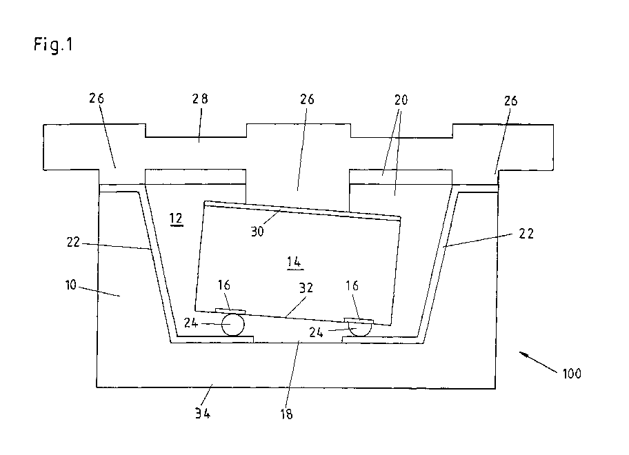
- the electrical or electronic component 100 shown in FIG. 1 is for use on one - not shown in Figures 1 and 2 for reasons of clarity
- Component 100 in this case becomes the connecting elements 24 before the component is implanted 14 in the flowable and malleable state - especially in the form of a liquid phase deposited drop of electrically conductive material - on the contact surface 16 of the component 14 applied to at least by subsequent deformation a part of the connecting elements 24, the position of the component 14 in the Recess 12 on the bottom region 18 of the recess 12 and especially on the contact surface 16 of the component 14 to adapt (alternatively, it is also possible to Connecting elements 24 before implanting the component 14 on the in the bottom area 18 of the recess 12 associated sections of the respective Apply contact track 22; each of the connecting elements 24 can also be implanted before of the component 14 advantageously partially on the in the bottom region 18 of the Recess 12 section of the contact track 22 and partially on the contact surface 16 of the component 14 are applied).
- the arrangement of the connecting elements 24 enables consequently a certain tilting of the component implanted in the recess 12 14 without the electrical contacting of the component 14, in particular the Contact surfaces 16 with the respective section of the assigned contact track 22 would suffer from it.
- the electrical or electronic Component 100 After sealing, a total of three are used to achieve a higher electrical Conductivity post-processed, electrically conductive contacts 26 on the sealed surface 28 of the carrier substrate 10 applied lithographically in order to contact the Realize the resulting electrical or electronic component 100 on a circuit board to be able to; in practice, the electrical or electronic component 100 will then soldered to the circuit board with reflow. It is enough for the electrical or electronic Component 100 has the particular advantage that, for example, for assembly a further coating is not required on a printed circuit board; rather, the electrical or electronic component 100 directly, that is to say without an additional adapter or carrier mounted on a circuit board.
- Electrically conductive contacts 26 is therefore an essential to the invention electrical or electronic component 100 that can be provided by electrical conductive contact surfaces both on its "front”, that is on the bottom and / or wall region 18 of the surface 12 of the component facing the recess 12 14, as well as on its "back”, that is, on the floor and / or wall area 18 of the recess 12 facing away from the surface of the component 14.
- electrical or electronic component 100 that can be provided by electrical conductive contact surfaces both on its "front”, that is on the bottom and / or wall region 18 of the surface 12 of the component facing the recess 12 14, as well as on its "back”, that is, on the floor and / or wall area 18 of the recess 12 facing away from the surface of the component 14.
- components 14 can both used with front contacts as well as with rear contacts are, for example active and / or passive electronic, optoelectronic, micromechanical and / or actuator components made of solid materials with semiconductor and / or with microsystem functions, with doping of the coating can be dispensed with in the form of the carrier substrate 10; can also by inserting and sealing the device 14 into the "bed" of the carrier material 10 and through leading out the electrical connections to the mounting of the component 14 Leadframes and the associated form, plating, trim, wrapping and wire bonding processes to be dispensed with.
- essential assembly steps are eliminated, as a result making electrical or electronic components 100 easier and less becomes costly.
- FIG. 2 relates to a method for producing a large number as an example in FIG 1 illustrated electrical or electronic components 100.
- the special feature here is it can be seen that a plurality of recesses 12 ("pockets") in a disc 36 (“wafer”) of a carrier substrate 10 made of semiconducting material (silicon) by etching is produced.
- This is followed by the above for each of the recesses 12 process steps described with reference to Figure 1, the end of the large number of resulting electrical or electronic components 100 by sawing the pane 36 is separated along the lines drawn in dashed lines in FIG. 2.
- This manufacturing process is characterized in particular by the fact that on the one hand Existing wafer technology is based, which reduces the development costs and risks and times are shorter than with a completely new technological development; on the other hand, the material of the component 14 and the material of the disk 36 have similar with identical material even identical thermal properties, which for the Function, for the life and for the reliability of the electrical or electronic Component 100 is of decisive advantage in that no different Thermal strains can occur and therefore a higher thermal load capacity is achieved.
Landscapes
- Structures For Mounting Electric Components On Printed Circuit Boards (AREA)
- Apparatuses And Processes For Manufacturing Resistors (AREA)
- Structures Or Materials For Encapsulating Or Coating Semiconductor Devices Or Solid State Devices (AREA)
- Wire Bonding (AREA)
- Internal Circuitry In Semiconductor Integrated Circuit Devices (AREA)
Abstract
Description
mindestens eine im Trägersubstrat vorgesehene Ausnehmung, insbesondere Kavität oder Vertiefung;
mindestens ein in der Ausnehmung implantiertes Bauelement, dessen mindestens eine elektrisch leitende Kontaktfläche aufweisende Oberfläche dem Boden- und/oder
Wandbereich der Ausnehmung zugewandt ist und im Boden- und/oder Wandbereich der Ausnehmung kontaktiert ist; und
mindestens ein Füllmaterial, mittels dessen das in der Ausnehmung implantierte Bauelement insbesondere mit den Rändern der Ausnehmung versiegelt ist.
- Fig. 1
- ein Ausführungsbeispiel eines elektrischen oder elektronischen Bauteils gemäß der vorliegenden Erfindung, im Querschnitt; und
- Fig. 2
- ein Ausführungsbeispiel einer mit einer Vielzahl von Ausnehmungen versehenen Platte oder Scheibe ("wafer") eines Trägersubstrats aus halbleitendem oder isolierendem Material, ebenfalls im Querschnitt.
- 100
- elektrisches oder elektronisches Bauteil
- 10
- Trägersubstrat aus halbleitendem oder isolierendem Material
- 12
- Ausnehmung, insbesondere Kavität oder Vertiefung
- 14
- Bauelement
- 16
- elektrisch leitende Kontaktfläche auf der dem Boden- und/oder Wandbereich 18 der Ausnehmung 12 zugewandten Oberfläche des Bauelements 14
- 18
- Boden- und/oder Wandbereich
- 20
- Füllmaterial
- 22
- elektrisch leitende Kontaktbahn
- 24
- elektrisch leitendes Verbindungselement
- 26
- elektrisch leitender Kontakt
- 28
- Oberfläche des Trägersubstrats 10
- 30
- elektrisch leitende Kontaktfläche auf der vom Boden- und/oder Wandbereich 18 der Ausnehmung 12 abgewandten Oberfläche des Bauelements 14
- 32
- Schutzschicht
- 34
- entgegengesetzte Fläche des Trägersubstrats 10
- 36
- Platte oder Scheibe ("wafer")
Claims (29)
- Elektrisches oder elektronisches Bauteil (100), aufweisend
ein Trägersubstrat (10) aus halbleitendem oder isolierendem Material;
mindestens eine im Trägersubstrat (10) vorgesehene Ausnehmung (12), insbesondere Kavität oder Vertiefung;
mindestens ein in der Ausnehmung (12) implantiertes Bauelement (14), dessen mindestens eine elektrisch leitende Kontaktfläche (16) aufweisende Oberfläche dem Boden- und/oder
Wandbereich (18) der Ausnehmung (12) zugewandt ist und im Boden- und/oder
Wandbereich (18) der Ausnehmung (12) kontaktiert ist; und
mindestens ein Füllmaterial (20), mittels dessen das in der Ausnehmung (12) implantierte Bauelement (14) insbesondere mit den Rändern der Ausnehmung (12) versiegelt ist;
dadurch gekennzeichnet, dass mindestens eine vom Boden- und/oder Wandbereich (18) der Ausnehmung (12) auf die Oberfläche (28) des Trägersubstrats (10) führende, elektrisch leitende Kontaktbahn (22) vorgesehen ist und
dass zwischen der jeweiligen Kontaktfläche (16) des Bauelements (14) und dem jeweiligen, sich im Boden- und/oder Wandbereich (18) der Ausnehmung (12) befindlichen Abschnitt der Kontaktbahn (22) mindestens ein elektrisch leitendes Verbindungselement (24) angeordnet ist, durch das die Kontaktfläche (16) des Bauelements (14) mit dem sich im Boden- und/oder Wandbereich (18) der Ausnehmung (12) befindlichen Abschnitt der Kontaktbahn (22) verbunden ist. - Bauteil gemäß Anspruch 1,
dadurch gekennzeichnet, dass die Ausnehmung (12) im wesentlichen muldenförmig oder trogförmig oder wannenförmig ausgebildet ist. - Bauteil gemäß Anspruch 1 oder 2,
dadurch gekennzeichnet, dass das Verbindungselement (24) aus elektrisch leitendem Material, insbesondere aus Lot, ist. - Bauteil gemäß mindestens einem der Ansprüche 1 bis 3,
dadurch gekennzeichnet, dass das Verbindungselement (24) im wesentlichen hügelförmig oder im wesentlichen kissenförmig oder im wesentlichen kugelförmig ist. - Bauteil gemäß mindestens einem der Ansprüche 1 bis 4,
dadurch gekennzeichnet, dass das Bauelement (14) mindestens ein IC-Chip (IC = integrated circuit = integrierte Schaltung) und/oder mindestens ein elektrisch aktiver oder elektronisch aktiver (Halbleiter-) Kristall ist. - Bauteil gemäß mindestens einem der Ansprüche 1 bis 5,
dadurch gekennzeichnet, dass das Füllmaterial (20) zum Versiegeln des in der Ausnehmung (12) implantierten Bauelements (14) Siliziumdioxid (SiO2) ist. - Bauteil gemäß mindestens einem der Ansprüche 1 bis 6,
dadurch gekennzeichnet, dass mindestens ein elektrisch leitender Kontakt (26) auf die versiegelte Oberfläche (28) des Trägersubstrats (10) aufgebracht, insbesondere lithographisch aufgebracht, ist. - Bauteil gemäß Anspruch 7,
dadurch gekennzeichnet, dass der Kontakt (26) nachbearbeitet ist. - Bauteil gemäß mindestens einem der Ansprüche 1 bis 8,
dadurch gekennzeichnet, dass das Bauelement (14) auf der vom Boden- und/oder Wandbereich (18) der Ausnehmung (12) abgewandten Oberfläche zumindest partiell mindestens eine elektrisch leitende Kontaktfläche (30) aufweist. - Bauteil gemäß Anspruch 9,
dadurch gekennzeichnet, dass die auf der vom Boden- und/oder Wandbereich (18) der Ausnehmung (12) abgewandten Oberfläche des Bauelements (14) zumindest partiell angeordnete Kontaktfläche (30) in Form mindestens einer Metallisierung ausgebildet ist. - Bauteil gemäß mindestens einem der Ansprüche 1 bis 10,
dadurch gekennzeichnet, dass das Bauelement (14) zumindest partiell mit mindestens einer Schutzschicht (32) versehen ist. - Bauteil gemäß Anspruch 11,
dadurch gekennzeichnet, dass die Schutzschicht (32) zumindest partiell auf der dem Boden- und/oder Wandbereich (18) der Ausnehmung (12) zugewandten Oberfläche des Bauelements (14) vorgesehen ist. - Leiterplatte (= PCB = printed circuit board), aufweisend mindestens ein elektrisches oder elektronisches Bauteil (100) gemäß mindestens einem der Ansprüche 1 bis 12.
- Verfahren zum Herstellen eines elektrischen oder elektronischen Bauteils (100), aufweisend die folgenden Schritte:dadurch gekennzeichnet, dass vor Implantieren des Bauelements (14) mindestens eine vom Boden- und/oder Wandbereich (18) der Ausnehmung (12) auf die Oberfläche (28) des Trägersubstrats (10) führende, elektrisch leitende Kontaktbahn (22) aufgebracht, insbesondere lithographisch aufgebracht, wird undErzeugen, insbesondere Ätzen, von mindestens einer Ausnehmung (12), insbesondere von mindestens einer Kavität oder Vertiefung, in einem Trägersubstrat (10) aus halbleitendem oder isolierendem Material;Implantieren von mindestens einem Bauelement (14), insbesondere von mindestens einem IC-Chip und/oder von mindestens einem elektrisch aktiven oder elektronisch aktiven (Halbleiter-)Kristall, in der Ausnehmung (12), wobei die mindestens eine elektrisch leitende Kontaktfläche (16) aufweisende Oberfläche des Bauelements (14) dem Boden- und/oder Wandbereich (18) der Ausnehmung (12) zugewandt ist und im Boden- und/oder Wandbereich (18) der Ausnehmung (12) kontaktiert wird; undVersiegeln des in der Ausnehmung (12) implantierten Bauelements (14) insbesondere mit den Rändern der Ausnehmung (12) mittels mindestens eines Füllmaterials (20);
dass mindestens ein, insbesondere zwei oder mehr elektrisch leitende Verbindungselemente (24) angeordnet werden, durch die die mindestens eine, insbesondere zwei oder mehr Kontaktflächen (16) des Bauelements (14) mit dem jeweiligen, sich im Boden- und/oder Wandbereich (18) der Ausnehmung (12) befindlichen Abschnitt der mindestens einen, insbesondere zwei oder mehr Kontaktbahnen (22) verbunden werden. - Verfahren gemäß Anspruch 14,
dadurch gekennzeichnet, dass das Verbindungselement (24) vor Implantieren des Bauelements (14) im fließfähigen und/oder formbaren Zustand angeordnet wird, um durch Verformen des Verbindungselements (24) die Position des Bauelements (14) in der Ausnehmung (12) an den Boden- und/oder Wandbereich (18) der Ausnehmung (12) und/oder an die Kontaktfläche (16) des Bauelements (14) anzupassen. - Verfahren gemäß Anspruch 14 oder 15,
dadurch gekennzeichnet, dass das Verbindungselement (24) vor Implantieren des Bauelements (14) auf den sich im Boden- und/oder Wandbereich (18) der Ausnehmung (12) befindlichen Abschnitt der Kontaktbahn (22) aufgebracht wird. - Verfahren gemäß mindestens einem der Ansprüche 14 bis 16,
dadurch gekennzeichnet, dass das Verbindungselement (24) vor Implantieren des Bauelements (14) auf die Kontaktfläche (16) des Bauelements (14) aufgebracht wird. - Verfahren gemäß mindestens einem der Ansprüche 14 bis 17,
dadurch gekennzeichnet, dass das Verbindungselement (24) vor Implantieren des Bauelements (14) teilweise auf den sich im Boden- und/oder Wandbereich (18) der Ausnehmung (12) befindlichen Abschnitt der Kontaktbahn (22) und teilweise auf die Kontaktfläche (16) des Bauelements (14) aufgebracht wird. - Verfahren gemäß mindestens einem der Ansprüche 14 bis 18,
dadurch gekennzeichnet, dass das Verbindungselement (24) vor Implantieren des Bauelements (14) aufgebracht wird, indem elektrisch leitendes Material insbesondere aus flüssiger Phase (beispielsweise Pilzgalvanik) oder insbesondere aus gasförmiger Phase abgeschieden wird. - Verfahren gemäß mindestens einem der Ansprüche 14 bis 19,
dadurch gekennzeichnet, dass das Verbindungselement (24) vor Implantieren des Bauelements (14) in Form mindestens eines Tropfens aus elektrisch leitendem Material aufgebracht wird, insbesondere durch Anschmelzen mindestens eines Metalldrahts. - Verfahren gemäß mindestens einem der Ansprüche 14 bis 20,
dadurch gekennzeichnet, dass der sich im Boden- und/oder Wandbereich (18) der Ausnehmung (12) befindliche Abschnitt der Kontaktbahn (22) und die Kontaktfläche (16) des Bauelements (14) durch das Verbindungselement (24) miteinander verlötet werden. - Verfahren gemäß mindestens einem der Ansprüche 14 bis 21,
dadurch gekennzeichnet, dass die Kontaktbahn (22) nachbearbeitet wird. - Verfahren gemäß mindestens einem der Ansprüche 14 bis 22,
dadurch gekennzeichnet, dass nach dem Versiegeln mindestens ein elektrisch leitender Kontakt (26) auf die versiegelte Oberfläche (28) des Trägersubstrats (10) aufgebracht, insbesondere lithographisch aufgebracht, wird. - Verfahren gemäß Anspruch 23,
dadurch gekennzeichnet, dass der Kontakt (26) nachbearbeitet wird. - Verfahren gemäß mindestens einem der Ansprüche 14 bis 24,
dadurch gekennzeichnet, dass vor Implantieren des Bauelements (14) zumindest partiell mindestens eine elektrisch leitende Kontaktfläche (30), insbesondere in Form mindestens einer Metallisierung, auf der vom Boden- und/oder Wandbereich (18) der Ausnehmung (12) abgewandten Oberfläche des Bauelements (14) aufgebracht wird. - Verfahren gemäß mindestens einem der Ansprüche 14 bis 25,
dadurch gekennzeichnet, dass vor Implantieren des Bauelements (14) zumindest partiell mindestens eine Schutzschicht (32) auf das Bauelement (14) aufgebracht wird. - Verfahren gemäß Anspruch 26,
dadurch gekennzeichnet, dass die Schutzschicht (32) zumindest partiell auf der dem Boden- und/oder Wandbereich (18) der Ausnehmung (12) zugewandten Oberfläche des Bauelements (14) aufgebracht wird. - Verfahren gemäß mindestens einem der Ansprüche 14 bis 27,
dadurch gekennzeichnet, dass nach dem Versiegeln und gegebenenfalls nach Testen des Bauelements (14) die der Oberfläche (28) des Trägersubstrats (10) entgegengesetzte Fläche (34) des Trägersubstrats (10) insbesondere mittels eines Lasers beschriftet wird. - Verfahren zum Herstellen einer Vielzahl elektrischer oder elektronischer Bauteile (100), insbesondere gemäß mindestens einem der Ansprüche 14 bis 28, gekennzeichnet durch die folgenden Schritte:Erzeugen, insbesondere Ätzen, einer Vielzahl von Ausnehmungen (12), insbesondere Kavitäten oder Vertiefungen, in einer Platte oder Scheibe (36; "wafer") eines Trägersubstrats (10) aus halbleitendem oder isolierendem Material;Aufbringen, insbesondere lithographisches Aufbringen, von jeweils mindestens einer vom Boden- und/oder Wandbereich (18) einer jeden Ausnehmung (12) auf die der jeweiligen Ausnehmung (12) zugeordnete Oberfläche (28) des Trägersubstrats (10) führenden, elektrisch leitenden Kontaktbahn (22);Anordnen von jeweils mindestens einem, insbesondere zwei oder mehr elektrisch leitenden Verbindungselementen (24) zum Verbinden von jeweils mindestens einer, insbesondere zwei oder mehr sich auf der Oberfläche eines Bauelements (14), insbesondere eines IC-Chips und/oder eines elektrisch aktiven oder elektronisch aktiven (Halbleiter-)Kristalls, befindlichen elektrisch leitenden Kontaktflächen (16) mit dem jeweiligen, sich im Boden- und/oder Wandbereich (18) der Ausnehmung (12) befindlichen Abschnitt der mindestens einen, insbesondere zwei oder mehr Kontaktbahnen (22);Implantieren von jeweils mindestens einem der Bauelemente (14) in jeder der Ausnehmungen (12), wobei die die Kontaktfläche (16) aufweisende Oberfläche des jeweiligen Bauelements (14) dem Boden- und/oder Wandbereich (18) der jeweiligen Ausnehmung (12) zugewandt ist und im Boden- und/oder Wandbereich (18) der Ausnehmung (12) kontaktiert wird;Versiegeln der in den Ausnehmungen (12) implantierten Bauelemente (14) insbesondere mit den Rändern der Ausnehmungen (12) mittels mindestens eines Füllmaterials (20); undVereinzeln der Vielzahl von Bauteilen (100), insbesondere durch mechanisches und/oder optisches Zersägen der Platte oder Scheibe (36).
Applications Claiming Priority (2)
| Application Number | Priority Date | Filing Date | Title |
|---|---|---|---|
| DE10047213A DE10047213A1 (de) | 2000-09-23 | 2000-09-23 | Elektrisches oder elektronisches Bauteil und Verfahren zum Herstellen desselben |
| DE10047213 | 2000-09-23 |
Publications (3)
| Publication Number | Publication Date |
|---|---|
| EP1198002A2 true EP1198002A2 (de) | 2002-04-17 |
| EP1198002A3 EP1198002A3 (de) | 2004-12-01 |
| EP1198002B1 EP1198002B1 (de) | 2009-04-15 |
Family
ID=7657383
Family Applications (1)
| Application Number | Title | Priority Date | Filing Date |
|---|---|---|---|
| EP01122430A Expired - Lifetime EP1198002B1 (de) | 2000-09-23 | 2001-09-20 | Elektrisches oder elektronisches Bauteil und Verfahren zum Herstellen desselben |
Country Status (4)
| Country | Link |
|---|---|
| US (1) | US6617677B2 (de) |
| EP (1) | EP1198002B1 (de) |
| JP (1) | JP2002141434A (de) |
| DE (2) | DE10047213A1 (de) |
Families Citing this family (13)
| Publication number | Priority date | Publication date | Assignee | Title |
|---|---|---|---|---|
| US7498196B2 (en) | 2001-03-30 | 2009-03-03 | Megica Corporation | Structure and manufacturing method of chip scale package |
| TW584950B (en) | 2001-12-31 | 2004-04-21 | Megic Corp | Chip packaging structure and process thereof |
| TW544882B (en) | 2001-12-31 | 2003-08-01 | Megic Corp | Chip package structure and process thereof |
| US6673698B1 (en) | 2002-01-19 | 2004-01-06 | Megic Corporation | Thin film semiconductor package utilizing a glass substrate with composite polymer/metal interconnect layers |
| TW503496B (en) * | 2001-12-31 | 2002-09-21 | Megic Corp | Chip packaging structure and manufacturing process of the same |
| US7187063B2 (en) | 2002-07-29 | 2007-03-06 | Yamaha Corporation | Manufacturing method for magnetic sensor and lead frame therefor |
| JP4659488B2 (ja) * | 2005-03-02 | 2011-03-30 | Okiセミコンダクタ株式会社 | 半導体装置及びその製造方法 |
| JP5107539B2 (ja) * | 2006-08-03 | 2012-12-26 | 新光電気工業株式会社 | 半導体装置および半導体装置の製造方法 |
| TWI351085B (en) * | 2006-08-08 | 2011-10-21 | Silicon Base Dev Inc | Structure and manufacturing method of package base for power semiconductor device |
| JP4955349B2 (ja) * | 2006-09-07 | 2012-06-20 | 新光電気工業株式会社 | 半導体装置 |
| US8106505B2 (en) | 2007-10-31 | 2012-01-31 | International Business Machines Corporation | Assembly including plural through wafer vias, method of cooling the assembly and method of fabricating the assembly |
| TWI624957B (zh) * | 2015-08-19 | 2018-05-21 | 乾坤科技股份有限公司 | 光電模組及其製造方法 |
| DE102020212424A1 (de) * | 2020-10-01 | 2022-04-07 | Robert Bosch Gesellschaft mit beschränkter Haftung | Laser-Bauelement und Verfahren zur Herstellung eines Laser-Bauelements |
Family Cites Families (11)
| Publication number | Priority date | Publication date | Assignee | Title |
|---|---|---|---|---|
| JPH0834264B2 (ja) * | 1987-04-21 | 1996-03-29 | 住友電気工業株式会社 | 半導体装置およびその製造方法 |
| EP0688051B1 (de) * | 1994-06-15 | 1999-09-15 | De La Rue Cartes Et Systemes | Herstellungsverfahren und Montage für IC-Karte. |
| US6013948A (en) * | 1995-11-27 | 2000-01-11 | Micron Technology, Inc. | Stackable chip scale semiconductor package with mating contacts on opposed surfaces |
| DE19720300B4 (de) | 1996-06-03 | 2006-05-04 | CiS Institut für Mikrosensorik gGmbH | Elektronisches Hybrid-Bauelement und Verfahren zu seiner Herstellung |
| US6329213B1 (en) * | 1997-05-01 | 2001-12-11 | Micron Technology, Inc. | Methods for forming integrated circuits within substrates |
| US5963429A (en) * | 1997-08-20 | 1999-10-05 | Sulzer Intermedics Inc. | Printed circuit substrate with cavities for encapsulating integrated circuits |
| KR100253363B1 (ko) * | 1997-12-02 | 2000-04-15 | 김영환 | 반도체 패키지용 기판과 그 기판을 이용한 랜드 그리드 어레이반도체 패키지 및 그들의 제조 방법 |
| FR2777675B1 (fr) * | 1998-04-15 | 2001-12-07 | Rue Cartes Et Systemes De | Procede de fabrication d'une carte a microcircuit et carte a microcircuit obtenue par mise en oeuvre de ce procede |
| KR100271656B1 (ko) * | 1998-05-30 | 2000-11-15 | 김영환 | 비지에이 반도체 패키지 및 그 제조방법 |
| US6133064A (en) * | 1999-05-27 | 2000-10-17 | Lsi Logic Corporation | Flip chip ball grid array package with laminated substrate |
| AU7748800A (en) * | 1999-09-30 | 2001-04-30 | Alpha Industries, Inc. | Semiconductor packaging |
-
2000
- 2000-09-23 DE DE10047213A patent/DE10047213A1/de not_active Withdrawn
-
2001
- 2001-09-20 DE DE50114834T patent/DE50114834D1/de not_active Expired - Lifetime
- 2001-09-20 EP EP01122430A patent/EP1198002B1/de not_active Expired - Lifetime
- 2001-09-21 JP JP2001289354A patent/JP2002141434A/ja not_active Withdrawn
- 2001-09-24 US US09/960,903 patent/US6617677B2/en not_active Expired - Fee Related
Also Published As
| Publication number | Publication date |
|---|---|
| EP1198002A3 (de) | 2004-12-01 |
| DE10047213A1 (de) | 2002-04-11 |
| US6617677B2 (en) | 2003-09-09 |
| EP1198002B1 (de) | 2009-04-15 |
| US20020142521A1 (en) | 2002-10-03 |
| DE50114834D1 (de) | 2009-05-28 |
| JP2002141434A (ja) | 2002-05-17 |
Similar Documents
| Publication | Publication Date | Title |
|---|---|---|
| DE10259221B4 (de) | Elektronisches Bauteil mit einem Stapel aus Halbleiterchips und Verfahren zur Herstellung desselben | |
| EP0860876A2 (de) | Anordnung und Verfahren zur Herstellung von CSP-Gehäusen für elektrische Bauteile | |
| WO2003019653A2 (de) | Verfahren zum kontaktieren und gehäusen von integrierten schaltungen | |
| EP3599636B1 (de) | Keramischer schaltungsträger und elektronikeinheit | |
| DE10110203B4 (de) | Elektronisches Bauteil mit gestapelten Halbleiterchips und Verfahren zu seiner Herstellung | |
| EP1532681A1 (de) | Mehrlagiger schaltungsträger und herstellung desselben | |
| DE19801312A1 (de) | Halbleiterbauelement mit mehreren Substratlagen und zumindest einem Halbleiterchip und einem Verfahren zum Herstellen eines solchen Halbleiterbauelementes | |
| EP1198002B1 (de) | Elektrisches oder elektronisches Bauteil und Verfahren zum Herstellen desselben | |
| EP1518267A2 (de) | Elektronisches bauteil mit einer gehäusepackung | |
| DE102019202715A1 (de) | Folienbasiertes package mit distanzausgleich | |
| DE19707887C2 (de) | Verfahren zum Herstellen und Trennen von elektronischen Elementen mit leitfähigen Kontaktanschlüssen | |
| DE19526511A1 (de) | Halbleitervorrichtung und Verfahren zu deren Herstellung und Montage | |
| DE10141571B4 (de) | Verfahren zum Zusammenbau eines Halbleiterbauelements und damit hergestellte integrierte Schaltungsanordnung, die für dreidimensionale, mehrschichtige Schaltungen geeignet ist | |
| DE102005046737A1 (de) | Bauteil mit Chip-Durchkontakten | |
| DE102005006280B4 (de) | Halbleiterbauteil mit einem Durchkontakt durch eine Gehäusemasse und Verfahren zur Herstellung desselben | |
| EP3774640A1 (de) | Bond-strukturen auf mems-element und asic-element | |
| EP2067390B1 (de) | Verfahren zur herstellung einer anordnung optoelektronischer bauelemente und anordnung optoelektronischer bauelemente | |
| DE4311762C2 (de) | Verfahren zur Verbindung elektrischer Kontaktstellen | |
| DE102009036033B4 (de) | Durchkontaktierung für Halbleiterwafer und Herstellungsverfahren | |
| DE102006024147B3 (de) | Elektronisches Modul mit Halbleiterbauteilgehäuse und einem Halbleiterchip und Verfahren zur Herstellung desselben | |
| DE10139985B4 (de) | Elektronisches Bauteil mit einem Halbleiterchip sowie Verfahren zu seiner Herstellung | |
| EP1285462B1 (de) | Halbleiterbauelement mit oberflächenmetallisierung | |
| EP1696481B1 (de) | Verfahren zur Integration eines elektronischen Bauteils in einer Substratkavität | |
| EP4084061A1 (de) | Schaltungsträger sowie verfahren zum herstellen einer elektrischen verbindung mit diesem | |
| DE19527611B4 (de) | Verfahren zum Herstellen eines Substrats für elektrische Schaltkreise |
Legal Events
| Date | Code | Title | Description |
|---|---|---|---|
| PUAI | Public reference made under article 153(3) epc to a published international application that has entered the european phase |
Free format text: ORIGINAL CODE: 0009012 |
|
| AK | Designated contracting states |
Kind code of ref document: A2 Designated state(s): AT BE CH CY DE DK ES FI FR GB GR IE IT LI LU MC NL PT SE TR |
|
| AX | Request for extension of the european patent |
Free format text: AL;LT;LV;MK;RO;SI |
|
| RAP1 | Party data changed (applicant data changed or rights of an application transferred) |
Owner name: PHILIPS CORPORATE INTELLECTUAL PROPERTY GMBH Owner name: KONINKLIJKE PHILIPS ELECTRONICS N.V. |
|
| RAP1 | Party data changed (applicant data changed or rights of an application transferred) |
Owner name: PHILIPS INTELLECTUAL PROPERTY & STANDARDS GMBH Owner name: KONINKLIJKE PHILIPS ELECTRONICS N.V. |
|
| PUAL | Search report despatched |
Free format text: ORIGINAL CODE: 0009013 |
|
| AK | Designated contracting states |
Kind code of ref document: A3 Designated state(s): AT BE CH CY DE DK ES FI FR GB GR IE IT LI LU MC NL PT SE TR |
|
| AX | Request for extension of the european patent |
Extension state: AL LT LV MK RO SI |
|
| RIC1 | Information provided on ipc code assigned before grant |
Ipc: 7H 01L 23/14 B Ipc: 7H 01L 23/053 B Ipc: 7H 01L 23/13 A Ipc: 7H 01L 23/057 B |
|
| 17P | Request for examination filed |
Effective date: 20050601 |
|
| AKX | Designation fees paid |
Designated state(s): DE FR GB |
|
| 17Q | First examination report despatched |
Effective date: 20050726 |
|
| RAP1 | Party data changed (applicant data changed or rights of an application transferred) |
Owner name: NXP B.V. |
|
| GRAP | Despatch of communication of intention to grant a patent |
Free format text: ORIGINAL CODE: EPIDOSNIGR1 |
|
| GRAP | Despatch of communication of intention to grant a patent |
Free format text: ORIGINAL CODE: EPIDOSNIGR1 |
|
| GRAS | Grant fee paid |
Free format text: ORIGINAL CODE: EPIDOSNIGR3 |
|
| GRAA | (expected) grant |
Free format text: ORIGINAL CODE: 0009210 |
|
| AK | Designated contracting states |
Kind code of ref document: B1 Designated state(s): DE FR GB |
|
| REG | Reference to a national code |
Ref country code: GB Ref legal event code: FG4D Free format text: NOT ENGLISH |
|
| REF | Corresponds to: |
Ref document number: 50114834 Country of ref document: DE Date of ref document: 20090528 Kind code of ref document: P |
|
| PLBE | No opposition filed within time limit |
Free format text: ORIGINAL CODE: 0009261 |
|
| STAA | Information on the status of an ep patent application or granted ep patent |
Free format text: STATUS: NO OPPOSITION FILED WITHIN TIME LIMIT |
|
| 26N | No opposition filed |
Effective date: 20100118 |
|
| PGFP | Annual fee paid to national office [announced via postgrant information from national office to epo] |
Ref country code: GB Payment date: 20120828 Year of fee payment: 12 |
|
| PGFP | Annual fee paid to national office [announced via postgrant information from national office to epo] |
Ref country code: FR Payment date: 20121004 Year of fee payment: 12 |
|
| GBPC | Gb: european patent ceased through non-payment of renewal fee |
Effective date: 20130920 |
|
| REG | Reference to a national code |
Ref country code: FR Ref legal event code: ST Effective date: 20140530 |
|
| PG25 | Lapsed in a contracting state [announced via postgrant information from national office to epo] |
Ref country code: GB Free format text: LAPSE BECAUSE OF NON-PAYMENT OF DUE FEES Effective date: 20130920 |
|
| PG25 | Lapsed in a contracting state [announced via postgrant information from national office to epo] |
Ref country code: FR Free format text: LAPSE BECAUSE OF NON-PAYMENT OF DUE FEES Effective date: 20130930 |
|
| PGFP | Annual fee paid to national office [announced via postgrant information from national office to epo] |
Ref country code: DE Payment date: 20140822 Year of fee payment: 14 |
|
| REG | Reference to a national code |
Ref country code: DE Ref legal event code: R119 Ref document number: 50114834 Country of ref document: DE |
|
| PG25 | Lapsed in a contracting state [announced via postgrant information from national office to epo] |
Ref country code: DE Free format text: LAPSE BECAUSE OF NON-PAYMENT OF DUE FEES Effective date: 20160401 |