EP1195810A1 - Aluminum-silicon carbide semiconductor substrate and method for producing the same - Google Patents
Aluminum-silicon carbide semiconductor substrate and method for producing the same Download PDFInfo
- Publication number
- EP1195810A1 EP1195810A1 EP01908348A EP01908348A EP1195810A1 EP 1195810 A1 EP1195810 A1 EP 1195810A1 EP 01908348 A EP01908348 A EP 01908348A EP 01908348 A EP01908348 A EP 01908348A EP 1195810 A1 EP1195810 A1 EP 1195810A1
- Authority
- EP
- European Patent Office
- Prior art keywords
- substrate
- component
- aluminum
- silicon carbide
- sic
- Prior art date
- Legal status (The legal status is an assumption and is not a legal conclusion. Google has not performed a legal analysis and makes no representation as to the accuracy of the status listed.)
- Granted
Links
Images



Classifications
-
- B—PERFORMING OPERATIONS; TRANSPORTING
- B22—CASTING; POWDER METALLURGY
- B22F—WORKING METALLIC POWDER; MANUFACTURE OF ARTICLES FROM METALLIC POWDER; MAKING METALLIC POWDER; APPARATUS OR DEVICES SPECIALLY ADAPTED FOR METALLIC POWDER
- B22F5/00—Manufacture of workpieces or articles from metallic powder characterised by the special shape of the product
-
- B—PERFORMING OPERATIONS; TRANSPORTING
- B22—CASTING; POWDER METALLURGY
- B22F—WORKING METALLIC POWDER; MANUFACTURE OF ARTICLES FROM METALLIC POWDER; MAKING METALLIC POWDER; APPARATUS OR DEVICES SPECIALLY ADAPTED FOR METALLIC POWDER
- B22F5/00—Manufacture of workpieces or articles from metallic powder characterised by the special shape of the product
- B22F5/006—Manufacture of workpieces or articles from metallic powder characterised by the special shape of the product of flat products, e.g. sheets
-
- C—CHEMISTRY; METALLURGY
- C22—METALLURGY; FERROUS OR NON-FERROUS ALLOYS; TREATMENT OF ALLOYS OR NON-FERROUS METALS
- C22C—ALLOYS
- C22C29/00—Alloys based on carbides, oxides, nitrides, borides, or silicides, e.g. cermets, or other metal compounds, e.g. oxynitrides, sulfides
- C22C29/02—Alloys based on carbides, oxides, nitrides, borides, or silicides, e.g. cermets, or other metal compounds, e.g. oxynitrides, sulfides based on carbides or carbonitrides
- C22C29/06—Alloys based on carbides, oxides, nitrides, borides, or silicides, e.g. cermets, or other metal compounds, e.g. oxynitrides, sulfides based on carbides or carbonitrides based on carbides, but not containing other metal compounds
- C22C29/065—Alloys based on carbides, oxides, nitrides, borides, or silicides, e.g. cermets, or other metal compounds, e.g. oxynitrides, sulfides based on carbides or carbonitrides based on carbides, but not containing other metal compounds based on SiC
-
- C—CHEMISTRY; METALLURGY
- C22—METALLURGY; FERROUS OR NON-FERROUS ALLOYS; TREATMENT OF ALLOYS OR NON-FERROUS METALS
- C22C—ALLOYS
- C22C32/00—Non-ferrous alloys containing at least 5% by weight but less than 50% by weight of oxides, carbides, borides, nitrides, silicides or other metal compounds, e.g. oxynitrides, sulfides, whether added as such or formed in situ
- C22C32/0047—Non-ferrous alloys containing at least 5% by weight but less than 50% by weight of oxides, carbides, borides, nitrides, silicides or other metal compounds, e.g. oxynitrides, sulfides, whether added as such or formed in situ with carbides, nitrides, borides or silicides as the main non-metallic constituents
- C22C32/0052—Non-ferrous alloys containing at least 5% by weight but less than 50% by weight of oxides, carbides, borides, nitrides, silicides or other metal compounds, e.g. oxynitrides, sulfides, whether added as such or formed in situ with carbides, nitrides, borides or silicides as the main non-metallic constituents only carbides
- C22C32/0063—Non-ferrous alloys containing at least 5% by weight but less than 50% by weight of oxides, carbides, borides, nitrides, silicides or other metal compounds, e.g. oxynitrides, sulfides, whether added as such or formed in situ with carbides, nitrides, borides or silicides as the main non-metallic constituents only carbides based on SiC
-
- H—ELECTRICITY
- H10—SEMICONDUCTOR DEVICES; ELECTRIC SOLID-STATE DEVICES NOT OTHERWISE PROVIDED FOR
- H10W—GENERIC PACKAGES, INTERCONNECTIONS, CONNECTORS OR OTHER CONSTRUCTIONAL DETAILS OF DEVICES COVERED BY CLASS H10
- H10W70/00—Package substrates; Interposers; Redistribution layers [RDL]
- H10W70/60—Insulating or insulated package substrates; Interposers; Redistribution layers
- H10W70/67—Insulating or insulated package substrates; Interposers; Redistribution layers characterised by their insulating layers or insulating parts
- H10W70/68—Shapes or dispositions thereof
- H10W70/6875—Shapes or dispositions thereof being on a metallic substrate, e.g. insulated metal substrates [IMS]
-
- H—ELECTRICITY
- H10—SEMICONDUCTOR DEVICES; ELECTRIC SOLID-STATE DEVICES NOT OTHERWISE PROVIDED FOR
- H10W—GENERIC PACKAGES, INTERCONNECTIONS, CONNECTORS OR OTHER CONSTRUCTIONAL DETAILS OF DEVICES COVERED BY CLASS H10
- H10W70/00—Package substrates; Interposers; Redistribution layers [RDL]
- H10W70/60—Insulating or insulated package substrates; Interposers; Redistribution layers
- H10W70/67—Insulating or insulated package substrates; Interposers; Redistribution layers characterised by their insulating layers or insulating parts
- H10W70/69—Insulating materials thereof
- H10W70/692—Ceramics or glasses
-
- H—ELECTRICITY
- H10—SEMICONDUCTOR DEVICES; ELECTRIC SOLID-STATE DEVICES NOT OTHERWISE PROVIDED FOR
- H10W—GENERIC PACKAGES, INTERCONNECTIONS, CONNECTORS OR OTHER CONSTRUCTIONAL DETAILS OF DEVICES COVERED BY CLASS H10
- H10W72/00—Interconnections or connectors in packages
- H10W72/30—Die-attach connectors
-
- H—ELECTRICITY
- H10—SEMICONDUCTOR DEVICES; ELECTRIC SOLID-STATE DEVICES NOT OTHERWISE PROVIDED FOR
- H10W—GENERIC PACKAGES, INTERCONNECTIONS, CONNECTORS OR OTHER CONSTRUCTIONAL DETAILS OF DEVICES COVERED BY CLASS H10
- H10W72/00—Interconnections or connectors in packages
- H10W72/851—Dispositions of multiple connectors or interconnections
- H10W72/874—On different surfaces
- H10W72/877—Bump connectors and die-attach connectors
-
- H—ELECTRICITY
- H10—SEMICONDUCTOR DEVICES; ELECTRIC SOLID-STATE DEVICES NOT OTHERWISE PROVIDED FOR
- H10W—GENERIC PACKAGES, INTERCONNECTIONS, CONNECTORS OR OTHER CONSTRUCTIONAL DETAILS OF DEVICES COVERED BY CLASS H10
- H10W72/00—Interconnections or connectors in packages
- H10W72/851—Dispositions of multiple connectors or interconnections
- H10W72/874—On different surfaces
- H10W72/879—Bump connectors and bond wires
-
- H—ELECTRICITY
- H10—SEMICONDUCTOR DEVICES; ELECTRIC SOLID-STATE DEVICES NOT OTHERWISE PROVIDED FOR
- H10W—GENERIC PACKAGES, INTERCONNECTIONS, CONNECTORS OR OTHER CONSTRUCTIONAL DETAILS OF DEVICES COVERED BY CLASS H10
- H10W72/00—Interconnections or connectors in packages
- H10W72/851—Dispositions of multiple connectors or interconnections
- H10W72/874—On different surfaces
- H10W72/884—Die-attach connectors and bond wires
-
- H—ELECTRICITY
- H10—SEMICONDUCTOR DEVICES; ELECTRIC SOLID-STATE DEVICES NOT OTHERWISE PROVIDED FOR
- H10W—GENERIC PACKAGES, INTERCONNECTIONS, CONNECTORS OR OTHER CONSTRUCTIONAL DETAILS OF DEVICES COVERED BY CLASS H10
- H10W74/00—Encapsulations, e.g. protective coatings
-
- H—ELECTRICITY
- H10—SEMICONDUCTOR DEVICES; ELECTRIC SOLID-STATE DEVICES NOT OTHERWISE PROVIDED FOR
- H10W—GENERIC PACKAGES, INTERCONNECTIONS, CONNECTORS OR OTHER CONSTRUCTIONAL DETAILS OF DEVICES COVERED BY CLASS H10
- H10W90/00—Package configurations
- H10W90/701—Package configurations characterised by the relative positions of pads or connectors relative to package parts
- H10W90/721—Package configurations characterised by the relative positions of pads or connectors relative to package parts of bump connectors
- H10W90/724—Package configurations characterised by the relative positions of pads or connectors relative to package parts of bump connectors between a chip and a stacked insulating package substrate, interposer or RDL
Definitions
- the present invention relates to a substrate on which semiconductor elements can be mounted and that is made of an aluminum-silicon carbide composite material. It also relates to a method for manufacturing the substrate, a package for semiconductor elements that uses the substrate, and a semiconductor device that uses the substrate.
- the heat-dissipating substrate has been required to reduce thermal strain caused at a combination interface between the semiconductor elements and peripheral members in a semiconductor package that contains the elements. Therefore, a thermal expansion coefficient of the heat-dissipating substrate that is equivalent to that of the semiconductor element and that of the peripheral member combined with the substrate is required.
- the thermal expansion coefficients of silicon (Si) and gallium arsenide (GaAs) that are each a semiconductor element are 4.2 and 6.5, respectively, in a unit of [10 -6 /°C].
- the thermal expansion coefficient of alumina (Al 2 O 3 ) that is a general-purpose peripheral member thereof is 6.5 in a unit of [10 -6 /°C].
- the thermal expansion coefficient of plastics is 12 through 17, which is relatively large, in a unit of [10 -6 /°C].
- a motherboard on which these are mounted is also plastic.
- Peripheral members, such as those mentioned above, have various levels of thermal expansion coefficients, and to correspond to these, the heat-dissipating substrate has employed a material whose thermal expansion coefficient is close to those of such peripheral members.
- Tungsien (W), molybdenum (Mo), copper (Cu), and these composite materials (Cu-W or Cu-Mo) have been used conventionally as materials for the heat-dissipating substrate, as disclosed by, for example, Japanese Published Unexamined Patent Application No. S52-59572 or Published Unexamined Patent Application No. H6-13494.
- these materials are expensive and heavy in weight.
- a motherboard on which the package is mounted is made of plastics small in rigidity, deformation will occur so as to cause difficulty in using the device if such a substrate is mounted on the motherboard. Similar to a ball grid array package (BGA package) described later, semiconductor equipment is recently connected to the motherboard by means of solder balls.
- BGA package ball grid array package
- solder balls will easily be damaged so as to be destroyed or deformed by the weight of the materials.
- a component for a package that is light in weight, that is excellent in matching a thermal expansion coefficient with peripheral members, and that is low cost is therefore in strong demand.
- the plastic package that has undergone a considerable reduction in size is in much higher demand for its weight reduction than the ceramic package.
- the degree of integration of semiconductor elements is small, and, accordingly, the amount of dissipated heat is also small. Therefore, a quad flat package (QFP) shown on the left side of Figure 1 has chiefly been used.
- QFP quad flat package
- FIG. 1 The left object in the figure is of the aforementioned QFP type.
- a semiconductor element 3 is packaged with a wire lead 2 and a lead pin 4, and the whole thereof is enclosed and sealed by sealing resin 6. This is used in a case where an actual capacity is less than at most 1W, and the number of terminals is within 250. If the actual capacity exceeds 3W, and the number of terminals rises up to 1000, a package having a ball grid array (BGA) structure is used like those next to the left object in Fig. 1. This structure needs a heat-dissipating substrate 1, to which the semiconductor element 3 is joined by die bonding.
- BGA ball grid array
- the element 3 is packaged with a wire lead, but a solder ball 5 is used as a terminal instead of a pin, in order to increase the packaging density.
- the heat-dissipating substrate 1 is a simple plate, in which a plastic substrate 7 is shaped like a frame for supporting it.
- the heat-dissipating substrate 1 is shaped like a lid integrated with a frame part, to which. the balls 5 are bonded with a tape 12.
- the number of terminals has exceeded 1000 as the actual capacity becomes larger, and thus the packaging structure has been changing to those shown at the rightmost side in Fig. 1.
- the semiconductor element is packaged according to a method that uses a flip chip (FC) 11, and the number of ball grids on the undersurface of the plastic substrate also has greatly increased.
- the heat-dissipating substrate 1 is a simple plate, and a frame-shaped metallic stiffener 10 serving to support the substrate 1 is disposed between the heat-dissipating substrate 1 and a plastic substrate 9 and is bonded to the two substrates with adhesive layers 8.
- the heat-dissipating substrate 1 is of the lid type, and the balls 5 are bonded to the substrate 1 by means of a tape 8.
- a member to be packaged such as a heat-dissipating substrate
- a member to be packaged is required to be light in weight and superior in thermal conductivity and be capable of easily coping with shape diversification or shape complexity.
- its size is being made even more compact, and its shape is becoming very diversified in relation to the combination with peripheral members.
- members that have high dimensional accuracy are required to be supplied at low cost and, in addition, the accuracy thereof must be maintained when practically used.
- members that are thinner in shape or are more complex in shape will be demanded in the future.
- a substrate has been conventionally manufactured by connecting or uniting a plurality of flat plates together.
- FIG. 2 shows one example thereof.
- Various forms of the heat-dissipating substrate are shown at the left of the figure.
- reference numerals are omitted except for the uppermost object.
- Each reference numeral designates the same component as that shown in Figure 1.
- the uppermost substrate is a conventional one shaped like a simple plate.
- the substrate is required to have a shape in which a fin is formed in the heat-dissipating area, as shown in the middle object next to the simple-plate-shaped substrate.
- lid type substrates provided with variously shaped cavity parts are needed depending on the position or size of a semiconductor element to be mounted.
- a fin is given to each of these substrates, they can be formed as shown at the middle of the figure.
- Packaging structures are Shown at the right of the figure.
- the semiconductor element is subjected to the flip chip packaging by use of the substrate provided with the fin as shown at the middle of the figure, and the resulting package is mounted onto a motherboard by the ball grid array.
- a frame stiffener In the uppermost structure, a frame stiffener must be interposed between the heat-dissipating substrate and the plastic substrate. Therefore, considerable time is consumed to package it, causing heat distortion to occur easily between the members because the connection parts increase. Accordingly, since the entire package is warped or deformed when packaged or operated, a reduction in reliability easily occurs.
- the drawback of metal chiefly composed of the latter, i.e., Al, is that the thermal expansion coefficient of pure Al is about 24 in a unit of [10 -6 /°C], which is very high relative to not only that of a semiconductor element but also to that of plastics, and in that deformation or damage occurs easily because of its softness. Due to these circumstances, recently, to a composite (Al-SiC) of silicon carbide (SiC), which is excellent in thermal conductivity and light in weight, and Al has drawn interest.
- the Al-SiC is manufactured according to an infiltration method in which Al is infiltrated into a porous body of SiC as described in Published Unexamined Patent Application No.
- the thermal expansion coefficient of A1 is about 24, and that of SiC is about 4 in a unit of [10 -6 /°C].
- a thermal expansion coefficient can be controlled within a wide range by changing the amount of both components, and making it light weight. Therefore, this is one of the suitable materials for a heat-dissipating substrate used for not only a plastic package but also various packages. For this reason, practical use as a component for a package is rapidly advancing.
- the composite material Al-SiC has several drawbacks as follows.
- the infiltration. method according to the sintering method, according to the casting method, or according to the dissolution method mentioned above, considerable time is consumed for the finish machining of a material after compositional processing is carried out, and, disadvantageously, tools wear out in a short time because SiC particles are hard. Therefore, if the component is simple in shape, this problem is relatively easy to solve, but if the shape of a package is further thinned, further complicated, and further diversified, this problem is exacerbated.
- the component is required to have higher dimensional accuracy in correlation with peripheral members, the provision of a material capable of simplifying its finish machining will be in strong demand. It is therefore an object of the present invention to inexpensively provide an Al-SiC semiconductor substrate that is superior in thermal performance and that is capable of stably maintaining high dimensional accuracy when practically used while coping with the current of rapid diversification of a practical shape. It is another object thereof to provide a package in which a semiconductor element using the substrate can be installed and provide a semiconductor device using the substrate.
- a substrate provided by the present invention is an aluminum-silicon carbide (Al-SiC) semiconductor substrate in which a first component is metal chiefly composed of aluminum (Al) and a second component is silicon carbide (SiC), wherein the second component is 5 to 60% by weight of the whole, and the remainder is the first component, and a warp in the direction of the main surface thereof is 3 ⁇ m/mm or less.
- Al-SiC aluminum-silicon carbide
- a manufacturing method for a semiconductor substrate of the present invention includes a step of preparing a composite material whose first component is metal chiefly composed of aluminum (Al) and whose second component is silicon carbide(SiC), wherein the second component is compositionally 5 to 60% by weight of the whole and the remainder is the first component, and a step of applying corrosion-resistant treatment onto a part of the composite material, thereafter bringing the composite material into contact with a corrosive, thereby removing a part other than the part subjected to the corrosion-resistant treatment, and shaping a form.
- the present invention includes a package that can contain a semiconductor element using the semiconductor substrate, and a semiconductor device using the substrate.
- Heat substrate 1 wire lead 2, semiconductor element 3, pin terminal 4, ball grid terminal 5, sealing resin layer 6, frame 7, adhesive layer 8, plastic substrate 9, stiffener 10, flip chip 11, adhesive layer 12, substrate sample 13, surface plate 14, laser source 15, laser beam 16, and motherboard 17.
- a semiconductor substrate of the present invention will be described hereinafter in relation to a manufacturing method thereof.
- An aluminum-silicon carbide (Al-SiC) composite material which is a material of the substrate of the present invention is manufactured according to the infiltration method, the sintering method, the casting method, the dissolution method, or a combination of these methods, as mentioned above.
- the infiltration method is a method for infiltrating the melted Al into the hole of a porous body made of SiC powder in a non-oxidizing atmosphere. Since there is a need to maintain the shape of the SiC porous body, the amount of SiC in the composite material obtained by this method is controlled to be within the range up to 60% by weight, in which the lower limit is 40% by weight.
- the sintering method is a method for mixing Al powder and SiC powder together at a desired composition ratio, and sintering a resulting molded piece at a temperature above the melting point of Al in a non-oxidizing atmosphere.
- the sintering process includes pressure means, such as forging, hot pressing, hot isostatic pressing (HIP), and hot extrusion.
- the amount of SiC in the composite material obtained by this method is controlled within the range of 5 to 60% by weight.
- the casting method is a method for casting molten Al and SiC powder into a mold, thereafter mixing them, and solidifying them.
- the dissolution method is a method for dispersing SiC particles into molten Al, thereafter sequentially and continuously cooling the dispersed ones, and compounding them.
- the amount of SiC in the composite material obtained by the casting method or the dissolution method is controlled within the range of 5 to 60% by weight.
- the reason why the lower limit of SiC is fixed at 5% by weight excluding the infiltration method is that there is almost no difference between the thermal expansion coefficient or the thermal conductivity of SiC and that of Al if the lower limit thereof is less than that value, and therefore the advantage of including SiC will be eliminated.
- the reason why the upper limit of SiC is fixed at 60% by weight in all of the above-mentioned methods is that the removal of the remaining SiC in corrosion treatment becomes difficult if the limit exceeds that value.
- the powder obtained after the mixture can be shaped like a sheet by thinly and directly applying plastic processing thereonto by means of a hot roll or the like according to the sintering method, for example.
- a plate material contemporarily compounded by the sintering method, by the casting method, or by the dissolution method can be again heated and can undergo plastic processing. If a large processing degree in thickness and in width is given by the plastic processing when the material is shaped like, for example, a sheet, it will be also possible to add slight heat treatment and remove residual stress after the plastic processing is completed.
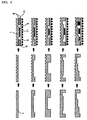
- the thus prepared Al-SiC composite material has its parts removed by a corrosive and takes on a form.
- This procedure will be hereinafter described with reference to an example of a flat plate made of the composite material.
- a center part i.e., part enclosed by the dotted line of the figure
- a corrosive that reacts to Al relatively slowly or that dissolves Al.
- a substance that is a metal salt solution and exhibits acescence or a substance in which oxygen ions are free is usually used as a suitable substance for such a corrosive.
- a weak solution of sulfate of copper more precious than Al, a weak solution of inorganic salt such as chloride, or a weak solution of organic salt such as copper acetate is used as that of a preferable metal salt.
- concentration of these materials in the solution is normally prepared to be 3 to 50% by weight. If it is less than the lower limit, too much time will be consumed for corrosion treatment. On the other hand, if it exceeds the upper limit, concavities/convexities will easily appear in a corroded removal part.
- a substance that exhibits alkalescence in water, such as sodium carbonate (Na 2 CO 3 ), may be mixed in as needed to finely adjust the pH of the corrosive and control the corrosion speed.
- Corrosion-resistant treatment that forms a coating layer of a desired pattern that can resist the corrosive prior to corrosion treatment is carried out to leave the part that has not been removed as it is.
- a material that is not eroded with the corrosive and is capable of easily adhering to a raw material is used as a material of the coating layer.
- resin or rubber is usually used. If rubber is used, a thin sheet of rubber is prepared, and is bonded to a part provided with a desired pattern with an adhesive that can resist the corrosive. Alternatively, an organic solvent that has dissolved rubber is applied to the surface of the raw material and is dried.
- the corrosive is sprayed onto the coating surface, or the raw material is soaked in the corrosive so as to bring them into contact with each other, and the necessary parts are gradually removed.
- the temperature of the corrosive can be higher than room temperature, but room temperature is sufficient to maintain the corrosive.
- only its surface can be removed by electrolytic polishing in which, for example, a raw material that has undergone corrosion-resistant treatment serves as an anode. If a material that has minute SiC particles is prepared beforehand in this case, a removal surface with extremely fine surface roughness can be obtained.
- a surface whose surface roughness Ra of JIS is below 2 ⁇ m or even below 1 ⁇ m easily can be obtained. Therefore, after the usual corrosion and removal is carried out, the process can be carried out to perform smooth finishing or to carve an extremely shallow concavo-convex part less than 5 ⁇ m. After the corrosion treatment is completed, the raw material is washed in water immediately, and residue is removed.
- the residue is removed therefrom. If slight surface finishing, which is usually employed, is needed, any removal method, such as barrel polishing or blast grinding, can be carried out.
- a predetermined main surface of penetration part can be formed in the raw material. Accordingly, when a small component having a predetermined shape is cut and separated from, for example, a plate material, this method can be used. In this case, grooves or concavities used for separation can be formed beforehand in the raw material. When a plurality of concave parts with various depths and convex parts with various heights are formed, they can be formed continuously or intermittently while being divided several times. According to the conventional method, machining is very difficult, and tools completely wear out. In contrast, according to the method of the present invention, it is relatively easy to carry out shape processing as described above, and, processing costs can advantageously be greatly lowered.
- the aluminum-silicon carbide (Al-SiC) semiconductor substrate of the present invention obtained by the above method leaves neither stress nor distortion because neither mechanical stress nor heat is given when level differences or concavities/convexities are provided although such mechanical stress or heat is given in the conventional grinding. Therefore, a warp in the direction of the main surface resulting after finish treatment is much smaller, i.e., below 3 ⁇ m/mm than conventional examples. Further, the substrate of the present invention can seldom cause a new warp or deformation resulting from residual stress because there is minimal residue after treatment even if mechanical stress or thermal stress is applied from the outside when it is contained in a package.
- the substrate of the present invention has high-strength against damage caused by fatigue in thermo-cycles during operation after the substrate is built in a semiconductor device. According to the method of the present invention, it is therefore, possible to provide a substrate that has a shape integrated into a complex form as mentioned above and that has a small warp or deformation after it is mounted or when actually operated. For example, during machine treatment, if concavities/convexities are partially formed in the substrate or if its outer periphery is complicated on the condition that its thickness is below 2 mm, the treatment will become extremely difficult, and the occurrence of a large warp or deformation cannot be avoided. For example, an external dimension thereof exceeding 30 mm will cause a warp or deformation that exceeds 10 ⁇ m/mm.
- a substrate having almost no warp or deformation can be obtained even if concavities/convexities are formed in its main surface that are wide and thin. Further, it is possible to manufacture a multi-piece substrate shaped like a tape in which perforations are formed in a sheet-shaped substrate by corrosion treatment.
- the semiconductor substrate of the present invention if the area of a part to be corroded and removed is below 50% of the entire main surface, such a warp level as mentioned above can be obtained even if it is substantially thin. For example, even if the ratio (t/A) of its thickness t to the area A of the main surface is below 0.008 in a unit of [mm/mm 2 ], a substrate having the above-mentioned warp level can be obtained. If the area of a part to be corroded and removed is below 30% of the entire main surface, such a warp level as mentioned above can be obtained even if the ratio is below 0.0008.
- the thickness t of the substrate of the present invention is defined not as the thickness of a part that has undergone corrosion treatment but as the thickness of a part that has not undergone treatment, and the area A of the main surface is defined not as the area of a part that has undergone the corrosion treatment but as the area of the entire main surface.
- the surface roughness of a to-be-removed part of the main surface of the present invention can be set at less than 5 ⁇ m in Ra by changing the pH of a corrosive liquid and controlling the corrosion speed as mentioned above.
- the present invention will hereinafter be described with reference to examples. It should be noted that the present invention is not limited to the scope of the examples.
- the preparation was made of silicon carbide powder consisting of crystal grains of 10 ⁇ m in average grain size, of above 99.9% in purity (mass base), and of the 6H type, pure aluminum powder that has been subjected to rapid solidification by melt atomization of 50 ⁇ m in average grain size and of above 99% in purity (mass base), and aluminum alloy powder that contains Si of 5% by weight that has been subjected to rapid solidification in the same way (in the following examples, this aluminum alloy is referred to simply as aluminum alloy).
- the amount of cation impurities, such as Fe, in the silicon carbide powder was below 100 ppm (mass base).
- Samples 1 through 8 and 12 are each a sample that uses pure aluminum as a first component
- Samples 9 through 11 are each a sample that uses aluminum alloy powder that contains Si of 5% by weight as a first component. Mixed slurry was subjected to spray drying and was granulated.
- This granular powder was molded into the shape of a plate of 50 mm in length and width and of 5 mm in thickness by means of dry powdery pressing. Thereafter, this molded piece was placed in a furnace under the high frequency induction heating method, and it was first gradually heated to 400°C in low-pressure nitrogen, and the binder was removed therefrom. Thereafter, the temperature was raised up to 665°C in ten minutes in a nitrogen gas stream of 1 atmospheric pressure, and the molded piece was kept at this temperature for three minutes, and it was preliminarily heated. Each sample that was subjected to the preliminary heating was moved to a preheated forging die of 300°C, and was subjected to hot forging.
- each composite material sample that has been forged were about 48 mm in length and width and about 4.8 mm in thickness. Therefore, the ratio t/A of the thickness to the area of the main surface is 0.002 [mm/mm 2 ].
- the relative density (i.e., the ratio of a measured density confirmed by the underwater method to a theoretical density) of each sample was 100%.
- the thermal conductivity and the thermal expansion coefficient were confirmed. The results are shown in Table I. The thermal conductivity was confirmed by the use of a disk-like test piece according to the laser flash method, and the thermal expansion coefficient was confirmed by the use of a pillar-like test piece according to the operating transformation method.
- Raw material compounding composition Composite material Formed body (% by weight) Thermal conductivity Thermal expansion coefficient Surface roughness Amount of warp ( ⁇ m/mm) First component Second component (W/m ⁇ K) (x 10 -6 /°C) Ra( ⁇ m) Removal surface Backside main surface 1 95 5 243 22.0 4.2 2.9 2.8 2 90 10 246 20.0 4.0 2.6 2.6 3 80 20 253 17.5 3.7 2.6 2.5 4 70 30 260 14.5 3.5 2.5 2.5 5 60 40 267 12.6 3.4 2.4 2.4 6 50 50 275 11.1 3.3 2.4 2.4 7 40 60 284 9.7 3.2 2.4 2.4 8 38 62 287 9.3 SiC particles remain in corroded parts; concavity/convexity size is large. 9 60 40 223 11.0 3.4 2.4 2.4 10 50 50 230 10.2 3.3 2.4 2.4 11 40 60 239 9.0 3.3 2.5 2.4 *12 60 40 267 12.6 3.4 5.9 6.3
- a concave part of 30 mm in length and width and 2 mm in depth was formed at the center of the main surface of each sample by corrosion treatment.
- the area ratio of the concave part to the main surface was 39%.
- Natural rubber was first dissolved in toluene, and was formed into a paste. This was applied to a part that does not undergo corrosion treatment to a thickness of 0.5 mm and was dried, and, as a result, a corrosion-resistant film was formed.
- Each sample was soaked into a copper sulfate solution of 8% by weight in concentration until the depth of the concave part became 2 mm at room temperature.
- Sample 12 of a comparative example where the composite material of Sample 5 is ground into the same shape with a diamond tool was also produced.
- the depth of the removed surface of a formed body that was obtained was within 2 mm ⁇ 0.05 mm in each sample.
- the surface roughness of the removed surface is shown in Table I by the value of Ra provided by JIS.
- the surface that was removed was confirmed by X-ray diffraction. As a result, SiC and Al were found.
- L( ⁇ m) is the minimum distance in the direction of the diagonal
- L o ( ⁇ m) is the maximum distance in the direction of the diagonal
- D(mm) is the scanning distance in the direction of the diagonal.
- finishing treatment can be carried out without allowing the SiC particles to remain on the treated surface after the corrosion treatment is completed.
- the warp in the direction of the main surface of the substrate increased by the cooling/heating cycle, however, in the sample that has undergone finishing treatment according to the present invention, a negligible increase in the warp was found before and after the cooling/heating cycle.
- the pure aluminum powder and the aluminum alloy powder were scaled by the amount corresponding to a pore volume of each molded piece, and were molded to have almost the same size in width and in length as the silicon carbide molded piece, and were used as an infiltrant of each molded piece sample.
- Each molded piece formed a thin layer of carbon (C) serving as an elution-resistant agent on all surfaces except one main surface that was brought into contact with the infiltrant when infiltrated.
- the molded piece was disposed on the corresponding infiltrant, and was kept in a nitrogen gas stream for one hour at 665°C, and each infiltrant was infiltrated in the pore of the molded piece.
- the width and length were 50 mm, and the thickness was 5 mm.
- the pure aluminum was infiltrated, and, in Samples 18 through 20, the aluminum alloy was infiltrated.
- blast finishing by the alumina bead was applied onto the surface where the infiltrant remained, and eluted-residues were removed.
- the relative density of the obtained infiltrated body was 100%. Those thermal conductivities and thermal expansion coefficients were confirmed as in Example 1. The results are shown in Table 11.
- Example 2 After the soak, the adhesive layer of the rubber layer was peeled off, as in Example 1. The removed part was subjected to blast finishing by an alumina bead of about 0.5 mm in diameter. As a result, the edge of the end of the removed part was removed.
- Sample 21 of a comparative example where the composite material of Sample 14 is ground into the same collar shape with a diamond tool in the same way as the above was also produced. The thickness of the collar part of a formed body that had been obtained was within 3 ⁇ 0.05 mm in each sample.
- the surface roughness of the removal surface is shown in Table I by the value of Ra provided by JIS. The surface that was removed was confirmed by X-ray diffraction. As a result, SiC and Al were found. No.
- finishing treatment can be carried out without allowing the SiC particles to remain on the treated surface after the corrosion treatment is completed.
- the warp in the direction of the main surface of the substrate increased by the cooling/heating cycle, but, in the sample that has undergone finishing treatment according to the present invention, a minimal increase in the warp was found before and after the cooling/heating cycle.
- the pure aluminum powder and the aluminum alloy powder were cast into a prepared graphite die cavity of 50 mm both in width and in length and 5 mm in depth, and were heated and melted in nitrogen at 700°C. Thereafter, the silicon carbide powder was cast into the molten metal, and was stirred for 30 minutes, and the silicon carbide powder particles were dispersed into the hot metal almost uniformly. Thereafter, they were cooled to room temperature.
- the molten metal of each composition ratio shown in Table III was solidified according to this method, and composite materials were produced.
- the solidified body removed the melted residue of the first component at the outer periphery by carrying out blast finishing with an alumina bead.
- the dimension of the composite material was 50 mm in length and in width and 5 mm in thickness, and the relative densities were completely 100%. Those thermal conductivities and thermal expansion coefficients were confirmed in the same way as in Example 1. Table III shows the results. In Samples 22 through 29 and 33 in the table, the first component indicates the pure aluminum, and, in Samples 30 through 32, the first component indicates the aluminum alloy.
- finishing treatment can be carried out without allowing the SiC particles to remain on the treated surface after the corrosion treatment is completed.
- the warp in the direction of the main surface of the substrate increased by the cooling/heating cycle, but, in the present invention, a change in the warp was hardly found before and after the cooling/heating cycle.
- the two kinds of packages are made of the same materials as those of Samples 5, 9, 14, and 26 among the samples of the above-mentioned examples and which employ the composite material of the present invention shown in Figure 6.
- Reference numeral 1 designates a simple planar heat-dissipating substrate that is made of the same material as that of each sample and that is 40 mm in length and width and 3 mm in thickness.
- Reference numeral 10 designates a stiffener that is 40 mm in outer length and outer width and 3 mm in thickness and that is made of electrolytic copper subjected to frame-like plastic processing (thermal expansion coefficient: 16.3 ⁇ 10 -6 /°C).
- Reference numeral 9 designates a plastic substrate that is 40 mm both in outer length and in outer width (thermal expansion coefficient: 12.6 ⁇ 10 -6 /°C).
- a Si semiconductor element 3 was joined to the heat-dissipating substrate by die bonding, and was mounted onto the plastic substrate according to a method using a flip chip 11.
- the stiffener 10 and the upper and lower substrates were joined together with an adhesive 8, and, likewise, the plastic substrate 9 and a ball grid 5 made of solder were joined together with the adhesive 8.
- (2) of Fig. 6 is a package of a second structure. The external dimensions thereof are the same as those of the first-structure package, and the stiffener part is integrated by a composition corresponding to the above-mentioned sample of the present invention. The difference is that the lid-shaped substrate 1 in which a cavity part has been excavated by the corrosion treatment of the present invention is used.
- the packaging of the Si semiconductor element is carried out in the same way as that of the first structure.
- the joining between the plastic substrate 9 and the frame of the heat-dissipating substrate 1 and between the ball grid 5 and the plastic substrate was carried out with the same adhesive as mentioned above.
- a package was manufactured that has the second structure and in which a cavity part has been excavated by grinding treatment of the composition/dimension corresponding to each sample mentioned above. For each sample mentioned above, 100 package samples were manufactured. Each sample package includes each sample mentioned above.
- Each of the package samples was heated for 20 minutes at 230°C, and was mounted on a plastic motherboard 17 (thermal expansion coefficient: 13.0 ⁇ 10 -6 /°C) by the solder ball grid 5, as shown on the right of Figure 6.
- This assembly was manufactured by the number (i.e., 100 pieces) of respective packages, and the state of deformation of the assembly caused when packaged was confirmed.
- lid made of the Al-SiC composite material of the present invention which has undergone the inside-excavation by corrosion treatment, whose thermal expansion coefficient is very close to that of the plastic substrate, and which has small residual distortion resulting from a small difference in the thermal expansion coefficient therebetween after the inside-excavation is carried out, was used. Therefore, damage at the interface between the lid and plastic substrate and defects resulting from the deformation of the two substrates were hardly observed when any kind of composite material was used.
- use was also made of the lid made of the Al-SiC composite material of the comparative example which is the same in material and which has undergone the inside-excavation by grinding treatment despite its thermal expansion coefficient being very close to that of the plastic substrate. As a result, damage at the interface between this and the plastic substrate and defects resulting from the deformation of the lid/substrate were caused. In this case, this kind of defect appeared in the ratio of 20 ⁇ 30 pieces to 100 pieces when any kind of composite material was used.
- a group of 10 assemblies of assemblies that were mounted with the above-mentioned structure and in which no defect was observed among the above-mentioned assemblies were attached to a semiconductor device, and they were continuously operated by the working output of 50W for 1000 hours.
- a decrease in output' was minimally observed.
- some of them demonstrated lowered output or some stopped working after a lapse of 300 to 500 hours.
- the heat-dissipating substrate can be combined with packaging members that are within a wide range corresponding to the substrate because the range of its thermal expansion coefficient is wide.
- the substrate can be satisfactorily used in combination with metal such as aluminum or copper when the materials of Samples 1 through 3 of Table I are used, and the substrate can be satisfactorily used in combination with ceramics, or the like, whose thermal expansion coefficient is relatively high when the materials such as Sample 11 of Table I are used.
- the substrate made of an Al-SiC composite material of the present invention to which finishing treatment, such as joggling or inside-excavation, has been applied not by machining but by corrosion treatment is cheaper in processing than machining. Since distortion or residual stress caused by processing when treated is minimal, defects do not appear, such as a warp, deformation, and damage, and are caused especially when it is mounted to a semiconductor package which includes a plastic substrate or that are caused by a cooling/heating load when it is actually working after it is mounted on a motherboard and is built in a semiconductor device. Therefore, it is possible to provide a semiconductor substrate that is light in weight, that is low cost compared to any conventional substrate, and that is high in reliability, to provide a semiconductor package that uses the substrate, and to provide a semiconductor device that uses the substrate.
Landscapes
- Engineering & Computer Science (AREA)
- Mechanical Engineering (AREA)
- Chemical & Material Sciences (AREA)
- Manufacturing & Machinery (AREA)
- Materials Engineering (AREA)
- Metallurgy (AREA)
- Organic Chemistry (AREA)
- Cooling Or The Like Of Semiconductors Or Solid State Devices (AREA)
- Ceramic Products (AREA)
- Carbon And Carbon Compounds (AREA)
Abstract
Description
| No. | Raw material compounding composition | Composite material | Formed body | ||||
| (% by weight) | Thermal conductivity | Thermal expansion coefficient | Surface roughness | Amount of warp (µm/mm) | |||
| First component | Second component | (W/m·K) | (x 10-6/°C) | Ra(µm) | Removal surface | Backside | |
| 1 | 95 | 5 | 243 | 22.0 | 4.2 | 2.9 | 2.8 |
| 2 | 90 | 10 | 246 | 20.0 | 4.0 | 2.6 | 2.6 |
| 3 | 80 | 20 | 253 | 17.5 | 3.7 | 2.6 | 2.5 |
| 4 | 70 | 30 | 260 | 14.5 | 3.5 | 2.5 | 2.5 |
| 5 | 60 | 40 | 267 | 12.6 | 3.4 | 2.4 | 2.4 |
| 6 | 50 | 50 | 275 | 11.1 | 3.3 | 2.4 | 2.4 |
| 7 | 40 | 60 | 284 | 9.7 | 3.2 | 2.4 | 2.4 |
| 8 | 38 | 62 | 287 | 9.3 | SiC particles remain in corroded parts; concavity/convexity size is large. | ||
| 9 | 60 | 40 | 223 | 11.0 | 3.4 | 2.4 | 2.4 |
| 10 | 50 | 50 | 230 | 10.2 | 3.3 | 2.4 | 2.4 |
| 11 | 40 | 60 | 239 | 9.0 | 3.3 | 2.5 | 2.4 |
| *12 | 60 | 40 | 267 | 12.6 | 3.4 | 5.9 | 6.3 |
| No. | Molded piece | Composite material | Formed body | |||||
| Porosity | Composition (% by weight) | Thermal conductivity | Thermal expansion coefficient | Surface roughness | Amount of warp (µ m/mm) | |||
| (%) | First component | Second component | (W/m·K) | (x 10-6/°C) | Ra(µm) | Removal surface | Backside main surface | |
| *13 | 66 | 62 | 38 | Impossible to produce it because the shape of the molded piece was deformed | ||||
| 14 | 64 | 60 | 40 | 275 | 11.8 | 3.3 | 2.6 | 2.6 |
| 15 | 54 | 50 | 50 | 282 | 10.8 | 3.2 | 2.5 | 2.6 |
| 16 | 44 | 40 | 60 | 290 | 8.9 | 3.2 | 2.5 | 2.6 |
| *17 | 53 | 37 | 63 | 293 | 8.7 | SiC particles remain in corroded parts; concavity/convexity size is large. | ||
| 18 | 63 | 60 | 40 | 230 | 11.0 | 3.3 | 2.4 | 2.5 |
| 19 | 53 | 50 | 50 | 290 | 9.9 | 3.2 | 2.5 | 2.6 |
| 20 | 45 | 40 | 60 | 240 | 8.9 | 3.2 | 2.5 | 2.6 |
| 21 | 64 | 60 | 40 | 230 | 11.8 | 3.3 | 6.1 | 6.4 |
| No. | Composite material | Formed body | |||||
| Composition (% by weight) | Thermal conductivity | Thermal expansion | Surface roughness | Amount of warp (µm/mm) | |||
| First component | Second component | (W/m·K) | (x 10-6/°C) | Ra(µm) | Removed surface | Backside main surface | |
| 22 | 95 | 5 | 231 | 22.3 | 4.7 | 2.9 | 2.7 |
| 23 | 90 | 10 | 235 | 20.2 | 4.1 | 2.8 | 2.7 |
| 24 | 80 | 20 | 241 | 17.8 | 3.8 | 2.7 | 2.6 |
| 25 | 70 | 30 | 252 | 14.9 | 3.7 | 2.6 | 2.6 |
| 26 | 60 | 40 | 259 | 12.9 | 3.7 | 2.6 | 2.6 |
| 27 | 50 | 50 | 265 | 11.4 | 3.6 | 2.5 | 2.6 |
| 28 | 40 | 60 | 277 | 9.3 | 3.4 | 2.5 | 2.5 |
| 29 | 38 | 62 | 280 | 9.0 | SiC particles remain in corroded parts; concavity/convexity size is large. | ||
| 30 | 60 | 40 | 217 | 11.4 | 3.5 | 2.5 | 2.5 |
| 31 | 50 | 50 | 224 | 10.7 | 3.5 | 2.5 | 2.5 |
| 32 | 40 | 60 | 230 | 9.0 | 3.4 | 2.5 | 2.5 |
| *33 | 60 | 40 | 259 | 12.9 | 3.7 | 5.6 | 5.8 |
Claims (6)
- An aluminum-silicon carbide semiconductor substrate whose first component is metal chiefly composed of aluminum and whose second component is silicon carbide, wherein the second component is compositionally 5 to 60% by weight of the whole and the remainder is the first component, and a warp in a direction of a main surface thereof is 3 µm/mm or less.
- The aluminum-silicon carbide semiconductor substrate of Claim 1, wherein a ratio (t/A) of a thickness (t) of the main surface to an area (A)thereof is 0.008 or less in a unit of [mm/mm2].
- The aluminum-silicon carbide semiconductor substrate of Claim 1 or Claim 2, wherein a surface ronghness of the main surface is 5 µm or less in Ra.
- A manufacturing method of an aluminum-silicon carbide semiconductor substrate whose first component is metal chiefly composed of aluminum and whose second component is silicon carbide, the method comprising: a step of preparing a composite material that consists of a second component of 5 to 60% by weight and a residue of a first component, the second component being silicon carbide, the first component being metal chiefly composed of aluminum; and a step of applying corrosion-resistant treatment to a part thereof, and removing at least a part except the part to which the corrosion-resistant treatment has been applied by contact thereof with a corrosive so as to produce a formed body.
- A package for a semiconductor element that uses the semiconductor substrate as recited in any one of Claims 1 through 3.
- A semiconductor device that uses the semiconductor substrate as recited in any one of Claims 1 through 3.
Applications Claiming Priority (3)
| Application Number | Priority Date | Filing Date | Title |
|---|---|---|---|
| JP2000072257 | 2000-03-15 | ||
| JP2000072257 | 2000-03-15 | ||
| PCT/JP2001/001727 WO2001069674A1 (en) | 2000-03-15 | 2001-03-05 | Aluminum-silicon carbide semiconductor substrate and method for producing the same |
Publications (3)
| Publication Number | Publication Date |
|---|---|
| EP1195810A1 true EP1195810A1 (en) | 2002-04-10 |
| EP1195810A4 EP1195810A4 (en) | 2007-10-10 |
| EP1195810B1 EP1195810B1 (en) | 2011-05-11 |
Family
ID=18590705
Family Applications (1)
| Application Number | Title | Priority Date | Filing Date |
|---|---|---|---|
| EP01908348A Expired - Lifetime EP1195810B1 (en) | 2000-03-15 | 2001-03-05 | Method for producing an aluminum-silicon carbide semiconductor substrate the same |
Country Status (3)
| Country | Link |
|---|---|
| US (1) | US6876075B2 (en) |
| EP (1) | EP1195810B1 (en) |
| WO (1) | WO2001069674A1 (en) |
Cited By (1)
| Publication number | Priority date | Publication date | Assignee | Title |
|---|---|---|---|---|
| WO2010084447A1 (en) * | 2009-01-23 | 2010-07-29 | Element Six Ltd | Method of treating a diamond containing body |
Families Citing this family (8)
| Publication number | Priority date | Publication date | Assignee | Title |
|---|---|---|---|---|
| JP4382547B2 (en) * | 2004-03-24 | 2009-12-16 | 株式会社アライドマテリアル | Semiconductor device substrate and semiconductor device |
| JP4764159B2 (en) * | 2005-12-20 | 2011-08-31 | 富士通セミコンダクター株式会社 | Semiconductor device |
| WO2007141851A1 (en) * | 2006-06-07 | 2007-12-13 | Fujitsu Limited | Semiconductor package and electronic apparatus |
| US8508036B2 (en) * | 2007-05-11 | 2013-08-13 | Tessera, Inc. | Ultra-thin near-hermetic package based on rainier |
| US7906376B2 (en) * | 2008-06-30 | 2011-03-15 | Intel Corporation | Magnetic particle-based composite materials for semiconductor packages |
| JP2012057252A (en) * | 2010-08-12 | 2012-03-22 | Denki Kagaku Kogyo Kk | Aluminum-silicon carbide composite material |
| US8865607B2 (en) | 2010-11-22 | 2014-10-21 | Saint-Gobain Ceramics & Plastics, Inc. | Infiltrated silicon carbide bodies and methods of making |
| CN102569234A (en) * | 2010-12-21 | 2012-07-11 | 中芯国际集成电路制造(北京)有限公司 | Ball grid array encapsulating structure and encapsulation method |
Family Cites Families (20)
| Publication number | Priority date | Publication date | Assignee | Title |
|---|---|---|---|---|
| JPS5259572A (en) | 1975-11-12 | 1977-05-17 | Hitachi Ltd | Electronic circuit device |
| JPS5921032A (en) | 1982-07-26 | 1984-02-02 | Sumitomo Electric Ind Ltd | Substrate for semiconductor device |
| US5167920A (en) | 1986-05-01 | 1992-12-01 | Dural Aluminum Composites Corp. | Cast composite material |
| US4786467A (en) | 1983-06-06 | 1988-11-22 | Dural Aluminum Composites Corp. | Process for preparation of composite materials containing nonmetallic particles in a metallic matrix, and composite materials made thereby |
| JPS617637A (en) * | 1984-06-22 | 1986-01-14 | Furukawa Electric Co Ltd:The | Semiconductor |
| US4746637A (en) | 1984-11-08 | 1988-05-24 | Kabushiki Kaisha Toshiba | Aluminum nitride sintered body and process for producing the same |
| US4796077A (en) * | 1986-08-13 | 1989-01-03 | Hitachi, Ltd. | Electrical insulating, sintered aluminum nitride body having a high thermal conductivity and process for preparing the same |
| US5000246A (en) | 1988-11-10 | 1991-03-19 | Lanxide Technology Company, Lp | Flotation process for the formation of metal matrix composite bodies |
| US5435825A (en) * | 1991-08-22 | 1995-07-25 | Toyo Aluminum Kabushiki Kaisha | Aluminum matrix composite powder |
| US5386329A (en) * | 1991-09-20 | 1995-01-31 | Victor Company Of Japan, Ltd. | Tape cassette loading system |
| JPH07105464B2 (en) | 1992-12-04 | 1995-11-13 | 住友電気工業株式会社 | Semiconductor device for mounting semiconductor elements |
| US5532513A (en) * | 1994-07-08 | 1996-07-02 | Johnson Matthey Electronics, Inc. | Metal-ceramic composite lid |
| JPH09157773A (en) | 1995-10-03 | 1997-06-17 | Hitachi Metals Ltd | Low thermal expansion / high thermal conductivity aluminum composite material and method for producing the same |
| JP4080030B2 (en) * | 1996-06-14 | 2008-04-23 | 住友電気工業株式会社 | Semiconductor substrate material, semiconductor substrate, semiconductor device, and manufacturing method thereof |
| JP3792790B2 (en) | 1996-07-23 | 2006-07-05 | キヤノン株式会社 | Vibration wave motor |
| JP2962466B2 (en) | 1997-01-06 | 1999-10-12 | 株式会社東芝 | Aluminum nitride sintered body |
| JP4071843B2 (en) | 1997-04-11 | 2008-04-02 | 住友電気工業株式会社 | Method for producing composite alloy member |
| KR100543836B1 (en) | 1997-08-19 | 2006-01-23 | 가부시키가이샤 히타치세이사쿠쇼 | Multichip Module Structure and Its Manufacturing Method |
| JP4304749B2 (en) | 1998-02-24 | 2009-07-29 | 住友電気工業株式会社 | Method for manufacturing member for semiconductor device |
| JPH11340385A (en) * | 1998-05-27 | 1999-12-10 | Furukawa Electric Co Ltd:The | Resin-sealed semiconductor device |
-
2001
- 2001-03-05 EP EP01908348A patent/EP1195810B1/en not_active Expired - Lifetime
- 2001-03-05 US US09/959,508 patent/US6876075B2/en not_active Expired - Lifetime
- 2001-03-05 WO PCT/JP2001/001727 patent/WO2001069674A1/en not_active Ceased
Cited By (1)
| Publication number | Priority date | Publication date | Assignee | Title |
|---|---|---|---|---|
| WO2010084447A1 (en) * | 2009-01-23 | 2010-07-29 | Element Six Ltd | Method of treating a diamond containing body |
Also Published As
| Publication number | Publication date |
|---|---|
| US6876075B2 (en) | 2005-04-05 |
| US20020195690A1 (en) | 2002-12-26 |
| EP1195810A4 (en) | 2007-10-10 |
| WO2001069674A1 (en) | 2001-09-20 |
| EP1195810B1 (en) | 2011-05-11 |
Similar Documents
| Publication | Publication Date | Title |
|---|---|---|
| US5086333A (en) | Substrate for semiconductor apparatus having a composite material | |
| KR100745872B1 (en) | Semiconductor substrate having copper/diamond composite material and method of making same | |
| JP4304749B2 (en) | Method for manufacturing member for semiconductor device | |
| EP1000915B1 (en) | Silicon carbide composite, method for producing it and heat dissipation device employing it | |
| EP2017886A1 (en) | Aluminum-silicon carbide composite body and method for processing the same | |
| EP1114807B1 (en) | Semiconductor device or heat dissipating substrate therefor using a composite material | |
| EP1113894A1 (en) | Functionally graded metal substrates and process for making same | |
| KR20080077094A (en) | Aluminum-silicon carbide composite and heat dissipation parts using the same | |
| CN113210611B (en) | Copper diamond composite material with metal layer coated on surface and preparation method and application thereof | |
| US6876075B2 (en) | Aluminum-silicon carbide semiconductor substrate and method for producing the same | |
| CN100353536C (en) | Semiconductor heat sink substrate, production method and assembly thereof | |
| JPWO2000076940A1 (en) | Composite material and semiconductor device using the same | |
| JP3818102B2 (en) | Heat dissipation substrate, method for manufacturing the same, and semiconductor device | |
| CN113149714A (en) | Aluminum diamond composite material with aluminum silicon carbide layer coated on surface and preparation method and application thereof | |
| JPH11307701A (en) | Heat dissipating board and manufacturing method thereof | |
| JP2000297301A (en) | Silicon carbide-based composite material, powder thereof, and production method thereof | |
| EP1174400A1 (en) | Porous silicon carbide sintered compact and silicon carbide metal composite suitable for use in table for wafer polishing machine | |
| JP2704932B2 (en) | Heat dissipation board, method of manufacturing the same, and semiconductor device | |
| JPWO2001069674A1 (en) | Aluminum-silicon carbide based semiconductor substrate and manufacturing method thereof | |
| JP4244210B2 (en) | Aluminum-ceramic composite and method for producing the same | |
| JP4275892B2 (en) | Manufacturing method of semiconductor element mounting substrate material | |
| JP4461513B2 (en) | Aluminum-silicon carbide based composite material and method for producing the same | |
| JPH1088272A (en) | Heat sink, manufacturing method thereof, and semiconductor device | |
| JP2002121639A (en) | Heat dissipation board and high power high frequency transistor package using it | |
| JP2815656B2 (en) | High-strength heat-radiating structural member for packaged semiconductor devices |
Legal Events
| Date | Code | Title | Description |
|---|---|---|---|
| PUAI | Public reference made under article 153(3) epc to a published international application that has entered the european phase |
Free format text: ORIGINAL CODE: 0009012 |
|
| 17P | Request for examination filed |
Effective date: 20011212 |
|
| AK | Designated contracting states |
Kind code of ref document: A1 Designated state(s): AT BE CH CY DE DK ES FI FR GB GR IE IT LI LU MC NL PT SE TR |
|
| RBV | Designated contracting states (corrected) |
Designated state(s): DE FR GB |
|
| A4 | Supplementary search report drawn up and despatched |
Effective date: 20070906 |
|
| 17Q | First examination report despatched |
Effective date: 20091103 |
|
| GRAP | Despatch of communication of intention to grant a patent |
Free format text: ORIGINAL CODE: EPIDOSNIGR1 |
|
| RTI1 | Title (correction) |
Free format text: METHOD FOR PRODUCING AN ALUMINUM-SILICON CARBIDE SEMICONDUCTOR SUBSTRATE THE SAME |
|
| GRAS | Grant fee paid |
Free format text: ORIGINAL CODE: EPIDOSNIGR3 |
|
| GRAA | (expected) grant |
Free format text: ORIGINAL CODE: 0009210 |
|
| AK | Designated contracting states |
Kind code of ref document: B1 Designated state(s): DE FR GB |
|
| REG | Reference to a national code |
Ref country code: GB Ref legal event code: FG4D |
|
| REG | Reference to a national code |
Ref country code: DE Ref legal event code: R096 Ref document number: 60144596 Country of ref document: DE Effective date: 20110622 |
|
| PLBE | No opposition filed within time limit |
Free format text: ORIGINAL CODE: 0009261 |
|
| STAA | Information on the status of an ep patent application or granted ep patent |
Free format text: STATUS: NO OPPOSITION FILED WITHIN TIME LIMIT |
|
| 26N | No opposition filed |
Effective date: 20120214 |
|
| REG | Reference to a national code |
Ref country code: DE Ref legal event code: R097 Ref document number: 60144596 Country of ref document: DE Effective date: 20120214 |
|
| REG | Reference to a national code |
Ref country code: FR Ref legal event code: PLFP Year of fee payment: 16 |
|
| REG | Reference to a national code |
Ref country code: FR Ref legal event code: PLFP Year of fee payment: 17 |
|
| REG | Reference to a national code |
Ref country code: FR Ref legal event code: PLFP Year of fee payment: 18 |
|
| PGFP | Annual fee paid to national office [announced via postgrant information from national office to epo] |
Ref country code: GB Payment date: 20200226 Year of fee payment: 20 Ref country code: DE Payment date: 20200218 Year of fee payment: 20 |
|
| PGFP | Annual fee paid to national office [announced via postgrant information from national office to epo] |
Ref country code: FR Payment date: 20200214 Year of fee payment: 20 |
|
| REG | Reference to a national code |
Ref country code: DE Ref legal event code: R071 Ref document number: 60144596 Country of ref document: DE |
|
| REG | Reference to a national code |
Ref country code: GB Ref legal event code: PE20 Expiry date: 20210304 |
|
| PG25 | Lapsed in a contracting state [announced via postgrant information from national office to epo] |
Ref country code: GB Free format text: LAPSE BECAUSE OF EXPIRATION OF PROTECTION Effective date: 20210304 |