EP1194021A2 - Method of producing multilayer printed wiring board and multilayer printed wiring board - Google Patents
Method of producing multilayer printed wiring board and multilayer printed wiring board Download PDFInfo
- Publication number
- EP1194021A2 EP1194021A2 EP01122596A EP01122596A EP1194021A2 EP 1194021 A2 EP1194021 A2 EP 1194021A2 EP 01122596 A EP01122596 A EP 01122596A EP 01122596 A EP01122596 A EP 01122596A EP 1194021 A2 EP1194021 A2 EP 1194021A2
- Authority
- EP
- European Patent Office
- Prior art keywords
- printed wiring
- wiring board
- insulating resin
- circuit pattern
- resin layer
- Prior art date
- Legal status (The legal status is an assumption and is not a legal conclusion. Google has not performed a legal analysis and makes no representation as to the accuracy of the status listed.)
- Withdrawn
Links
Images




Classifications
-
- H—ELECTRICITY
- H05—ELECTRIC TECHNIQUES NOT OTHERWISE PROVIDED FOR
- H05K—PRINTED CIRCUITS; CASINGS OR CONSTRUCTIONAL DETAILS OF ELECTRIC APPARATUS; MANUFACTURE OF ASSEMBLAGES OF ELECTRICAL COMPONENTS
- H05K3/00—Apparatus or processes for manufacturing printed circuits
- H05K3/46—Manufacturing multilayer circuits
- H05K3/4644—Manufacturing multilayer circuits by building the multilayer layer by layer, i.e. build-up multilayer circuits
-
- H—ELECTRICITY
- H05—ELECTRIC TECHNIQUES NOT OTHERWISE PROVIDED FOR
- H05K—PRINTED CIRCUITS; CASINGS OR CONSTRUCTIONAL DETAILS OF ELECTRIC APPARATUS; MANUFACTURE OF ASSEMBLAGES OF ELECTRICAL COMPONENTS
- H05K3/00—Apparatus or processes for manufacturing printed circuits
- H05K3/40—Forming printed elements for providing electric connections to or between printed circuits
- H05K3/42—Plated through-holes or plated via connections
- H05K3/423—Plated through-holes or plated via connections characterised by electroplating method
-
- H—ELECTRICITY
- H05—ELECTRIC TECHNIQUES NOT OTHERWISE PROVIDED FOR
- H05K—PRINTED CIRCUITS; CASINGS OR CONSTRUCTIONAL DETAILS OF ELECTRIC APPARATUS; MANUFACTURE OF ASSEMBLAGES OF ELECTRICAL COMPONENTS
- H05K1/00—Printed circuits
- H05K1/02—Details
- H05K1/09—Use of materials for the conductive, e.g. metallic pattern
-
- H—ELECTRICITY
- H05—ELECTRIC TECHNIQUES NOT OTHERWISE PROVIDED FOR
- H05K—PRINTED CIRCUITS; CASINGS OR CONSTRUCTIONAL DETAILS OF ELECTRIC APPARATUS; MANUFACTURE OF ASSEMBLAGES OF ELECTRICAL COMPONENTS
- H05K2201/00—Indexing scheme relating to printed circuits covered by H05K1/00
- H05K2201/03—Conductive materials
- H05K2201/0332—Structure of the conductor
- H05K2201/0335—Layered conductors or foils
- H05K2201/0344—Electroless sublayer, e.g. Ni, Co, Cd or Ag; Transferred electroless sublayer
-
- H—ELECTRICITY
- H05—ELECTRIC TECHNIQUES NOT OTHERWISE PROVIDED FOR
- H05K—PRINTED CIRCUITS; CASINGS OR CONSTRUCTIONAL DETAILS OF ELECTRIC APPARATUS; MANUFACTURE OF ASSEMBLAGES OF ELECTRICAL COMPONENTS
- H05K2201/00—Indexing scheme relating to printed circuits covered by H05K1/00
- H05K2201/03—Conductive materials
- H05K2201/0332—Structure of the conductor
- H05K2201/0335—Layered conductors or foils
- H05K2201/0355—Metal foils
-
- H—ELECTRICITY
- H05—ELECTRIC TECHNIQUES NOT OTHERWISE PROVIDED FOR
- H05K—PRINTED CIRCUITS; CASINGS OR CONSTRUCTIONAL DETAILS OF ELECTRIC APPARATUS; MANUFACTURE OF ASSEMBLAGES OF ELECTRICAL COMPONENTS
- H05K2201/00—Indexing scheme relating to printed circuits covered by H05K1/00
- H05K2201/03—Conductive materials
- H05K2201/0332—Structure of the conductor
- H05K2201/0388—Other aspects of conductors
- H05K2201/0394—Conductor crossing over a hole in the substrate or a gap between two separate substrate parts
-
- H—ELECTRICITY
- H05—ELECTRIC TECHNIQUES NOT OTHERWISE PROVIDED FOR
- H05K—PRINTED CIRCUITS; CASINGS OR CONSTRUCTIONAL DETAILS OF ELECTRIC APPARATUS; MANUFACTURE OF ASSEMBLAGES OF ELECTRICAL COMPONENTS
- H05K2201/00—Indexing scheme relating to printed circuits covered by H05K1/00
- H05K2201/09—Shape and layout
- H05K2201/09209—Shape and layout details of conductors
- H05K2201/095—Conductive through-holes or vias
- H05K2201/09563—Metal filled via
-
- H—ELECTRICITY
- H05—ELECTRIC TECHNIQUES NOT OTHERWISE PROVIDED FOR
- H05K—PRINTED CIRCUITS; CASINGS OR CONSTRUCTIONAL DETAILS OF ELECTRIC APPARATUS; MANUFACTURE OF ASSEMBLAGES OF ELECTRICAL COMPONENTS
- H05K3/00—Apparatus or processes for manufacturing printed circuits
- H05K3/10—Apparatus or processes for manufacturing printed circuits in which conductive material is applied to the insulating support in such a manner as to form the desired conductive pattern
- H05K3/108—Apparatus or processes for manufacturing printed circuits in which conductive material is applied to the insulating support in such a manner as to form the desired conductive pattern by semi-additive methods; masks therefor
-
- H—ELECTRICITY
- H05—ELECTRIC TECHNIQUES NOT OTHERWISE PROVIDED FOR
- H05K—PRINTED CIRCUITS; CASINGS OR CONSTRUCTIONAL DETAILS OF ELECTRIC APPARATUS; MANUFACTURE OF ASSEMBLAGES OF ELECTRICAL COMPONENTS
- H05K3/00—Apparatus or processes for manufacturing printed circuits
- H05K3/38—Improvement of the adhesion between the insulating substrate and the metal
- H05K3/388—Improvement of the adhesion between the insulating substrate and the metal by the use of a metallic or inorganic thin film adhesion layer
-
- H—ELECTRICITY
- H05—ELECTRIC TECHNIQUES NOT OTHERWISE PROVIDED FOR
- H05K—PRINTED CIRCUITS; CASINGS OR CONSTRUCTIONAL DETAILS OF ELECTRIC APPARATUS; MANUFACTURE OF ASSEMBLAGES OF ELECTRICAL COMPONENTS
- H05K3/00—Apparatus or processes for manufacturing printed circuits
- H05K3/46—Manufacturing multilayer circuits
- H05K3/4602—Manufacturing multilayer circuits characterized by a special circuit board as base or central core whereon additional circuit layers are built or additional circuit boards are laminated
-
- H—ELECTRICITY
- H05—ELECTRIC TECHNIQUES NOT OTHERWISE PROVIDED FOR
- H05K—PRINTED CIRCUITS; CASINGS OR CONSTRUCTIONAL DETAILS OF ELECTRIC APPARATUS; MANUFACTURE OF ASSEMBLAGES OF ELECTRICAL COMPONENTS
- H05K3/00—Apparatus or processes for manufacturing printed circuits
- H05K3/46—Manufacturing multilayer circuits
- H05K3/4611—Manufacturing multilayer circuits by laminating two or more circuit boards
- H05K3/4623—Manufacturing multilayer circuits by laminating two or more circuit boards the circuit boards having internal via connections between two or more circuit layers before lamination, e.g. double-sided circuit boards
-
- Y—GENERAL TAGGING OF NEW TECHNOLOGICAL DEVELOPMENTS; GENERAL TAGGING OF CROSS-SECTIONAL TECHNOLOGIES SPANNING OVER SEVERAL SECTIONS OF THE IPC; TECHNICAL SUBJECTS COVERED BY FORMER USPC CROSS-REFERENCE ART COLLECTIONS [XRACs] AND DIGESTS
- Y10—TECHNICAL SUBJECTS COVERED BY FORMER USPC
- Y10T—TECHNICAL SUBJECTS COVERED BY FORMER US CLASSIFICATION
- Y10T29/00—Metal working
- Y10T29/49—Method of mechanical manufacture
- Y10T29/49002—Electrical device making
- Y10T29/49117—Conductor or circuit manufacturing
-
- Y—GENERAL TAGGING OF NEW TECHNOLOGICAL DEVELOPMENTS; GENERAL TAGGING OF CROSS-SECTIONAL TECHNOLOGIES SPANNING OVER SEVERAL SECTIONS OF THE IPC; TECHNICAL SUBJECTS COVERED BY FORMER USPC CROSS-REFERENCE ART COLLECTIONS [XRACs] AND DIGESTS
- Y10—TECHNICAL SUBJECTS COVERED BY FORMER USPC
- Y10T—TECHNICAL SUBJECTS COVERED BY FORMER US CLASSIFICATION
- Y10T29/00—Metal working
- Y10T29/49—Method of mechanical manufacture
- Y10T29/49002—Electrical device making
- Y10T29/49117—Conductor or circuit manufacturing
- Y10T29/49124—On flat or curved insulated base, e.g., printed circuit, etc.
- Y10T29/49126—Assembling bases
-
- Y—GENERAL TAGGING OF NEW TECHNOLOGICAL DEVELOPMENTS; GENERAL TAGGING OF CROSS-SECTIONAL TECHNOLOGIES SPANNING OVER SEVERAL SECTIONS OF THE IPC; TECHNICAL SUBJECTS COVERED BY FORMER USPC CROSS-REFERENCE ART COLLECTIONS [XRACs] AND DIGESTS
- Y10—TECHNICAL SUBJECTS COVERED BY FORMER USPC
- Y10T—TECHNICAL SUBJECTS COVERED BY FORMER US CLASSIFICATION
- Y10T29/00—Metal working
- Y10T29/49—Method of mechanical manufacture
- Y10T29/49002—Electrical device making
- Y10T29/49117—Conductor or circuit manufacturing
- Y10T29/49124—On flat or curved insulated base, e.g., printed circuit, etc.
- Y10T29/49128—Assembling formed circuit to base
-
- Y—GENERAL TAGGING OF NEW TECHNOLOGICAL DEVELOPMENTS; GENERAL TAGGING OF CROSS-SECTIONAL TECHNOLOGIES SPANNING OVER SEVERAL SECTIONS OF THE IPC; TECHNICAL SUBJECTS COVERED BY FORMER USPC CROSS-REFERENCE ART COLLECTIONS [XRACs] AND DIGESTS
- Y10—TECHNICAL SUBJECTS COVERED BY FORMER USPC
- Y10T—TECHNICAL SUBJECTS COVERED BY FORMER US CLASSIFICATION
- Y10T29/00—Metal working
- Y10T29/49—Method of mechanical manufacture
- Y10T29/49002—Electrical device making
- Y10T29/49117—Conductor or circuit manufacturing
- Y10T29/49124—On flat or curved insulated base, e.g., printed circuit, etc.
- Y10T29/49155—Manufacturing circuit on or in base
-
- Y—GENERAL TAGGING OF NEW TECHNOLOGICAL DEVELOPMENTS; GENERAL TAGGING OF CROSS-SECTIONAL TECHNOLOGIES SPANNING OVER SEVERAL SECTIONS OF THE IPC; TECHNICAL SUBJECTS COVERED BY FORMER USPC CROSS-REFERENCE ART COLLECTIONS [XRACs] AND DIGESTS
- Y10—TECHNICAL SUBJECTS COVERED BY FORMER USPC
- Y10T—TECHNICAL SUBJECTS COVERED BY FORMER US CLASSIFICATION
- Y10T29/00—Metal working
- Y10T29/49—Method of mechanical manufacture
- Y10T29/49002—Electrical device making
- Y10T29/49117—Conductor or circuit manufacturing
- Y10T29/49124—On flat or curved insulated base, e.g., printed circuit, etc.
- Y10T29/49155—Manufacturing circuit on or in base
- Y10T29/49156—Manufacturing circuit on or in base with selective destruction of conductive paths
-
- Y—GENERAL TAGGING OF NEW TECHNOLOGICAL DEVELOPMENTS; GENERAL TAGGING OF CROSS-SECTIONAL TECHNOLOGIES SPANNING OVER SEVERAL SECTIONS OF THE IPC; TECHNICAL SUBJECTS COVERED BY FORMER USPC CROSS-REFERENCE ART COLLECTIONS [XRACs] AND DIGESTS
- Y10—TECHNICAL SUBJECTS COVERED BY FORMER USPC
- Y10T—TECHNICAL SUBJECTS COVERED BY FORMER US CLASSIFICATION
- Y10T29/00—Metal working
- Y10T29/49—Method of mechanical manufacture
- Y10T29/49002—Electrical device making
- Y10T29/49117—Conductor or circuit manufacturing
- Y10T29/49124—On flat or curved insulated base, e.g., printed circuit, etc.
- Y10T29/49155—Manufacturing circuit on or in base
- Y10T29/49165—Manufacturing circuit on or in base by forming conductive walled aperture in base
Definitions
- the present invention relates to a method of producing a multilayer printed wiring board and to a multilayer printed wiring board produced by the method of producing a multilayer printed wiring board.
- a laminate-en-bloc method in which a plurality of double-sided substrates, as core substrates, each having a specified circuit pattern formed on each side are laminated and adhesive bonded en bloc through prepreg.
- Another is a build-up method in which a specified circuit pattern and an insulating resin layer are formed one after another.
- a substrate formed by laminating copper foil to cloth or non-woven fabric made of glass or aramide impregnated with epoxy resin or phenol resin, i.e., a copper clad laminate is used as a core substrate.
- Through holes are formed in the copper clad laminate by drilling or laser, first, and then are made to be electrically conductive by copper-plating. Thereafter, the copper foil is formed into a specified circuit pattern by etching, to thereby produce a double-sided substrate. Sequentially, two or more double-sided substrates thus produced are laminated and adhesive bonded to each other through prepreg to thereby produce a multilayer printed wiring board.
- a copper clad laminate having a specified circuit pattern formed thereon or a multilayer printed wiring board produced by the laminate-en-bloc method is used as the core substrate.
- Insulating resin is coated on the core substrate, first, and, then, via holes for interconnecting layers are formed by a photo lithography or laser. Then, copper plating is performed to form a specified circuit pattern and also make the via holes be electrically conductive.
- the specified circuit pattern and the insulating resin layer are alternately formed by alternating the insulating resin coating step and the copper plating step, whereby a multilayer printed wiring board is produced.
- the core substrate used is formed with a cloth or non-woven fabric, it is hard to reduce thickness and weight of the printed wiring board and diameter of the through holes for a high-dense wiring.
- the build-up method since the cloth or non-woven fabric is not present in the insulating resin layer, the insulating resin layer can be reduced in thickness and via holes can be reduced in diameter.
- the build-up method has some advantage over the laminate-en-bloc method in the intended purpose of providing a low-profile, light-weight and high-density wiring of a printed wiring board.
- it is still hard to provide a low-profile, light-weight and high-density wiring of the core substrate.
- the present invention provides a novel method of producing a multilayer printed wiring board comprising a step of forming an insulating resin layer on a metal foil; a step of forming a via hole in the insulating resin layer; a step of forming a specified circuit pattern on the insulating resin layer and forming a conductive layer in the via hole, by plating; and a step of etching the metal foil to form it into the specified circuit pattern.
- a multilayer printed wiring board intended to have a low-profile, light-weight and high-density wiring of the printed wiring board can be produced.
- the metal foil is made of any of copper or copper alloy containing copper as its primary component, nickel or nickel alloy containing nickel as its primary component, alloy containing nickel and iron as its primary components and stainless steel.
- the insulating resin layer comprises polyimide.
- the present invention includes a multilayer printed wiring board produced in a method of producing a multilayer printed wiring board comprising a step of forming an insulating resin layer on a metal foil; a step of forming a via hole in the insulating resin layer; a step of forming a specified circuit pattern on the insulating resin layer and forming a conductive layer in the via hole, by plating; and a step of etching the metal foil to form it into the specified circuit pattern.
- This multilayer printed wiring board can be intended to have a low-profile, light-weight and high-density wiring of a printed wiring board as has been increasingly demanded in recent years.
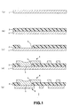
- an insulating resin layer is formed on a metal foil, first.
- a metal foil 1 is prepared and then the front surface of the metal foil 1 is degreased and is roughened, as required.
- metal foil 1 Any metals having good electrical conducting properties may be used as the metal foil 1.
- copper or copper alloy containing copper as its primary component, nickel or nickel alloy containing nickel as its primary component, aluminum or aluminum alloy containing aluminum as its primary component and alloy containing nickel and iron as its primary components may preferably be used.
- the alloy containing nickel and iron as its primary components a total of more than 90 weight% of nickel and iron is preferably contained in the whole alloy and further 20-90 weight%, or preferably 36-85 weight% of nickel is preferably contained in the whole alloy.
- nickel content 85 weight%, 78 weight%, 45 weight%, 42 weight% and 36 weight% are commercially available as the alloy containing nickel and iron as its primary components.
- a stainless steel having elasticity For the purpose of providing an increased bending strength of a finished multilayer printed wiring board, for example a stainless steel having elasticity can be used.
- the metal foil 1 it is enough for the metal foil 1 to have thickness of a few ⁇ m or more at least. If a higher bending strength is required, then the metal foil 1 having thickness of more than 100 ⁇ m may be used, depending on the number of metal foils used for forming the multilayer printed wiring board.
- the metal foil 1 may be degreased with any known acidic or alkaline degreasing agent, for example, by heating at temperature ranging from room temperature to 60°C for a few minutes, unless the metal foil 1 is made of aluminum or aluminum alloy.
- degreasing agents are Metaclea CL-5513 (available from Dai-ichi Kogyo Seiyaku Co., Ltd.) and OPC Acid-clean 115 (available from Okuno Chemical Industries Co., Ltd.).
- the degreasing agents ranging from acid to weak alkali should preferably be used.
- An example of those degreasing agents is Toparclean 161 (available from Okuno Chemical Industries Co., Ltd.).
- the metal foil 1 is roughened for the purpose of improving adhesiveness between the metal foil 1 and the insulating resin sequentially formed on the metal foil 1.
- Commercially available surface roughening agents may be used for the surface roughening of the metal foil 1.
- CZ-8100 available from Mec. Co., Ltd.
- OPC-400 available from Okuno Chemical Industries Co., Ltd.
- the surface roughening of the metal foil 1 may be omitted when the insulating resin used has adequate adhesion properties to the metal foil 1.
- an insulating resin layer 2 is formed on the single side of the metal foil 1 thus degreased and roughened, as required, by use of insulating resin.
- the insulating resins that may be used include generally available build-up insulating resins. Either of wet resin form (liquid form) and dry film form can be used as the insulating resin.
- the insulating resin layer 2 may be formed on the metal foil 1 by applying the insulating resin of liquid form to the single side of the metal foil 1 or by laminating the insulating resin of dry film form on the single side of the metal foil 1.
- insulating resins of liquid form is BL-9700 (available from Hitachi Chemical Co., Ltd.) and an example of the insulating resins of dry film form is BF-8500 (available from Hitachi Chemical Co., Ltd.).
- No particular limitation is imposed on the primary component of the insulating resins.
- epoxy, phenol, polyimide and BT resin can be used as the primary component of the insulating resins.
- polyimide is preferably used.
- polyimide When polyimide is used as the primary component of the insulating resin, e.g. Kapton (available from Du Pont-Toray Co., Ltd.), UPILEX (available from Ube Industries, Ltd.) or a like insulating resin may be laminated on the single side of the metal foil 1 through adhesive such as SPB-050A (available from Nippon Steel Chemical Co., Ltd.), to form the insulating layer 2.
- adhesive such as SPB-050A (available from Nippon Steel Chemical Co., Ltd.)
- polyamic acid solution is applied to the single side of the metal foil 1 and then is cured by heating, to form the insulating resin layer 2 of polyimide.
- the insulating resin layer 2 thus formed is required to have thickness enough to ensure the interlayer insulation reliability.
- the thickness of the insulating resin layer 2 can selectively be determined in the range of e.g. a few ⁇ m to some tens ⁇ m.
- via holes 3 are formed in the insulating resin layer 2 and, if necessary, the front surface of the insulating resin layer 2 is roughened.
- the via holes 3 are formed to electrically connect between the layers.
- the via holes 3 are formed in the insulating resin layer 2 in a laser method generally used in the build-up method.
- the via holes 3 can be formed by the photo lithography to subject the photosensitive resin to exposure and development.
- the surface roughening of the insulating resin layer 2 can be provided by using a commercially available desmear agent containing permanganate as the primary component, depending on a kind of the insulating resin layer 2 used.
- the first circuit pattern 4 is formed on the insulating resin layer 2 and conductive layers 5 are formed in the via holes 3, both of which are formed by plating.
- the method for forming the first circuit pattern 4 on the insulating resin layer 2 is not limited to any particular method.
- Known circuit-pattern forming methods such as a subtractive method, a semi-additive method and a full-additive method, may be used for forming a specified circuit pattern.
- the conductive layers 5 are formed in the via holes 3 by plating, to allow the metal foil 1 and the first circuit pattern 4 to be electrically conductive through the conductive layers 5.
- Either of electrolysis plating and electroless plating may be used for forming the circuit pattern 4 and the conductive layer 5.
- the copper is preferably used.
- a via filling additive and the like should preferably be added, for facilitation of filling of the plating into the via holes 3.
- the thickness of the first circuit pattern 4 thus formed can selectively be determined in the range of e.g. a few ⁇ m to some tens ⁇ m.
- the metal foil 1 is etched to form the second circuit pattern 6, as shown in FIG. 1(e), whereby the double-sided substrate 7 is produced.
- the metal foil 1 is etched in the following process, for example.
- a dry film resist is formed on the front surface of the metal foil 1 in the same pattern as the second circuit pattern 6, first, and, then, the metal foil 1 is etched. Thereafter, the dry film resist is peeled off.
- the double-sided substrate 7 thus produced has the structure wherein the first circuit pattern 4 and the second circuit pattern 6 are electrically connected to each other through the conductive layers 5.
- a printed wiring(s) is/are layered thereon through an adhesion sheet(s) such as prepreg or is/are layered on an either side or both sides of the double-sided substrate 7 by the build-up method, to thereby produce a multilayer printed wiring board.
- the multilayer printed wiring board thus produced provides a low-profile, light-weight and high-density wiring, and as such can fully meet the needs of the low-profile, light-weight and high-density wiring of the printed wiring board as have been increasingly demanded in recent years.
- a sequence of steps for forming the double-sided substrate 7 as mentioned above may be changed as follows. For example, after the insulating resin layer 2 is preformed, the metal foil 1 is laminated to that preformed insulating resin layer 2. Further, after the via holes 3 are formed on that preformed insulating resin layer 2, the insulating resin layer 2 having the preformed via holes 3 and the metal foil 1 are laminated to each other. In addition, the etching of the metal foil 1 may be performed at any time after the insulating resin layer 2 is laminated on the metal foil 1.
- a rolled nickel foil having thickness of 25 ⁇ m (Ni-H available from Toyo Seihaku Co., Ltd.) was cut out to a desired size and was treated with a degreasing agent (50ml/L-Metaclea CL-5513 available from Dai-ichi Kogyo Seiyaku Co., Ltd.) at 60°C for 2 minutes. Then, this was washed with water and dried.
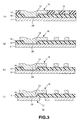
- a nickel foil 11 was prepared, as shown in FIG. 2(a).
- a photosensitive photovia ink (BL-9700 available from Hitachi Chemical Co., Ltd.) was applied to a single side of the nickel foil 11 by a screen printing with a polyester screen of 200 mesh/inch. Then, this was dried in a dryer of 80°C for 40 minutes.
- the insulating resin layer 12 having thickness of about 30 ⁇ m was formed, as shown in FIG. 2(b).
- the front surface of the insulating resin layer 12 was roughened by desmear agents (MLB-497 available from Meltex, Inc.) of 70°C for 10 minutes and then was washed with water. Thereafter, it was treated with neutralizing agent of 60°C (MLB-790 available from Meltex, Inc.) for 5 minutes and then was washed with water. Further, it was treated with plating catalyst (HS-202B available from Hitachi Chemical Co., Ltd.) for 5 minutes to allow the plating catalyst to adhere to the insulating resin layer 12. After having been washed with water, this was treated with activation liquid (ADP-601 available from Hitachi Chemical Co., Ltd.) for 5 minutes. Then, it was washed with water and then dried.
- desmear agents MB-497 available from Meltex, Inc.
- a dry film resist 15 (SPG-152 available from Asahi Chemical Industry Co., Ltd.) was laminated on a front surface of the nickel plated layer 14 at 110°C. Then, after a film mask was put in close contact with the dry film resist, it was irradiated with ultraviolet of 120mJ/cm 2 from the extra-high pressure mercury vapor lamp. Thereafter, it was treated by 10g/L-sodium carbonate of 30°C being sprayed over it at a pressure of 0.1MPa for 20 seconds and then was washed with water. Through these steps, the dry film resist 15 was formed in an opposite circuit pattern to a first circuit pattern 16 described below, as shown in FIG. 2(e).
- the copper plating was performed at a current density of 2.5A/dm 2 for 20 minutes by using copper sulfate plating solution (additive of 0.2ml/L-CC-1220 available from Japan Energy Corporation) and thereby the first circuit pattern 16 of about 10 ⁇ m in thickness and a conductive layer 29 in the via hole 13 were formed, as shown in FIG. 3(f).
- copper sulfate plating solution additive of 0.2ml/L-CC-1220 available from Japan Energy Corporation
- the dry film resist (SPG-152 available from Asahi Chemical Industry Co., Ltd.) was laminated on a front surface of the nickel foil 11 at 110°C. Then, after the film mask was put in close contact with the dry film resist, it was irradiated with ultraviolet of 120mJ/cm 2 from the extra-high pressure mercury vapor lamp. Thereafter, it was treated by 10g/L-sodium carbonate of 30°C being sprayed over it at a pressure of 0.1MPa for 20 seconds and then was washed with water. Through these steps, the dry film resist was formed in an identical circuit pattern to a second circuit pattern 17 described below.
- One layer was built up on each side of the double-sided substrate 18 to thereby produce a four-layer printed wiring board.
- copper roughening agent CZ-8100 available from Mec. Co., Ltd.
- CZ-8100 available from Mec. Co., Ltd.
- 35°C was sprayed over a front surface of the first circuit pattern 16 at a pressure of 0.1MPa for 30 seconds, first, and then it was washed with water. Thereafter, this was treated with 350ml/L-hydrochloric acid of 30°C at a pressure of 0.1MPa for 30 seconds and then was washed with water and dried. Through these steps, the front surface of the first circuit pattern 16 was roughened.
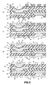
- the photosensitive photovia ink (BL-9700 available from Hitachi Chemical Co., Ltd.) was applied to the first circuit pattern 16 by the screen printing with a polyester screen of 150 mesh/inch. Then, this was dried in the dryer of 80°C for 40 minutes. Through these steps, an insulating resin layer 19 having thickness of about 30 ⁇ m was formed on the first circuit pattern 16, as shown in FIG. 4(a).
- the photosensitive photovia ink (BL-9700 available from Hitachi Chemical Co., Ltd.) was applied to the second circuit pattern 17 by the screen printing with a polyester screen of 100 mesh/inch. Then, this was dried in the dryer of 90°C for 40 minutes. Through these steps, an insulating resin layer 20 having thickness of about 30 ⁇ m was formed on the second circuit pattern 17, as shown in FIG. 4(b).
- the both surfaces of the insulating resin layers 19, 20 were roughened by the desmear agent (MLB-497 available from Meltex, Inc.) of 70°C for 10 minutes and then were washed with water. Thereafter, they were treated with the neutralizing agent (MLB-790 available from Meltex, Inc.) of 60°C for 5 minutes and then were washed with water. Further, they were treated with the plating catalyst (HS-202B available from Hitachi Chemical Co., Ltd.) for 5 minutes to allow the plating catalyst to adhere to the insulating resin layers 19, 20. After having been washed with water, these were treated with activation liquid (ADP-601 available from Hitachi Chemical Co., Ltd.) for 5 minutes. Then, they were washed with water and then dried.
- MMB-497 available from Meltex, Inc.
- dry film resists 25, 26 (SPG-152 available from Asahi Chemical Industry Co., Ltd.) were laminated on front surfaces of the nickel plated layers 23, 24 at 110°C. Then, after film masks were put in close contact with the dry film resists, they were irradiated with ultraviolet of 120mJ/cm 2 from the extra-high pressure mercury vapor lamp. Thereafter, these were treated by 10g/L-sodium carbonate of 30°C being sprayed over them at a pressure of 0.1MPa for 20 seconds and then was washed with water. Through these steps, the dry film resists 25, 26 were formed in opposite circuit patterns to third and fourth circuit patterns 27, 28 described below, as shown in FIG. 5(e).
- the copper plating was performed at a current density of 2.5A/dm 2 for 20 minutes by using the copper sulfate plating solution (additive of 0.2ml/L-CC-1220 available from Japan Energy Corporation) and thereby the third and fourth circuit patterns 27, 28 of about 10 ⁇ m in thickness and conductive layers 30, 33 in the via holes 21, 22 were formed, as shown in FIG. 5(f).
- the copper sulfate plating solution additive of 0.2ml/L-CC-1220 available from Japan Energy Corporation
- a rolled copper alloy foil having thickness of 35 ⁇ m (C-7025 available from Yamaha-Olin Metal Corporation) was cut out to a desired size and was treated with a degreasing agent (200ml/L-OPC Acid clean 115 available from Okuno Chemical Industries Co., Ltd.) at 60°C for 2 minutes. Then, it was washed with water and dried. Through these steps, a copper alloy foil 31 was prepared, as shown in FIG. 6(a).
- the copper alloy foil 31 was immersed into 100ml/L -hydrochlonic acid of 30°C for 20 seconds and then was immersed into palladium-substituted plating solution (200ml/L-ICP Accela available from Okuno Chemical Industries Co., Ltd.) of 30°C for 3 minutes. Then, it was washed with water. Further, this was immersed into the electroless nickel plating solution (B-1 available from Meltex, Inc.) of 60°C for 2 minutes, and then it was washed with water and dried. Through these steps, a nickel plated layer 32 having thickness of about 0.1 ⁇ m was formed on a single side of the copper alloy foil 31, as shown in FIG. 6(b).
- polyamic acid resin solution of the composition shown below was applied to the front surface of the nickel plated layer 32 of the copper alloy foil 31 by use of a spin coater. Then, it was dried in the dryer of 100°C for 15 minutes and then was cured in the dryer under nitrogen gas atmosphere of 400°C for 1 hour. Through these steps, an insulating resin layer 34 having thickness of about 10 ⁇ m was formed, as shown in FIG. 6(c).
- Diamine p-phenylenediamine 5 parts by weight
- Solvent N-methyl-2-pyrrolidone 28 parts by weight
- via holes 35 having a diameter of about 50 ⁇ m were formed in the insulating resin layer 34 by use of a laser drilling device (MODEL 5200 available from ESI Corporation) in the conditions of frequency of 4kHz, output power of 700mW, and 50 shots/hole, as shown in FIG. 6(d).
- a laser drilling device MODEL 5200 available from ESI Corporation
- a chrome sputter deposit 36 having thickness of about 0.03 ⁇ m was formed in the conditions of argon gas and RF power of 400W and, sequentially, a copper sputter deposit 37 having thickness of about 0.1 ⁇ m was formed in the conditions of argon gas and RF power of 300W, as shown in FIG. 6(e).
- a dry film resist 39 (SPG-152 available from Asahi Chemical Industry Co., Ltd.) was laminated on a front surface of the copper plated layer 38 at 110°C. Then, after a film mask was put in close contact with the dry film resist, it was irradiated with ultraviolet of 120mJ/cm 2 from the extra-high pressure mercury vapor lamp. Thereafter, it was treated by 10g/L-sodium carbonate of 30°C being sprayed over it at a pressure of 0.1MPa for 20 seconds and then was washed with water. Through these steps, the dry film resist 39 was formed in an identical circuit pattern to a first circuit pattern 40 described below, as shown in FIG. 7(g).
- the dry film resist (SPG-152 available from Asahi Chemical Industry Co., Ltd.) was laminated on a front surface of the copper alloy foil 31 at 110°C. Then, after the film mask was put in close contact with the dry film resist, it was irradiated with ultraviolet of 120mJ/cm 2 from the extra-high pressure mercury vapor lamp. Thereafter, it was treated by 10g/L-sodium carbonate of 30°C being sprayed over it at a pressure of 0.1MPa for 20 seconds and then was washed with water. Through these steps, the dry film resist was formed in an identical circuit pattern to a second circuit pattern 41 described below.
- Two double-sided substrates 42 thus produced which were different in circuit pattern from each other, were laminated and adhesive bonded to each other to thereby produce a four-layer printed wiring board.
- two double-sided substrates 42 (one of them has the same circuit pattern as the double-sided substrate 18 formed thereon) were prepared. They were immersed into the copper roughening solution (200g/L-ammonium persulfate) of 30°C for 1 minute and then washed with water and dried. Through these steps, the front surface of the first circuit pattern 40 and the front surface of the second circuit pattern 41 were roughened.
- the copper roughening solution 200g/L-ammonium persulfate
- the two double-sided substrates 42 were laminated and bonded to each other via polyimide resin adhesive 44 (SPB-050A available from Nippon Steel Chemical Co., Ltd.) sandwiched therebetween for 60 minutes in the conditions of 200°C and 3MPa by use of a vacuum press, to thereby produce the four-layer printed wiring board as shown in FIG. 8(b).
- SPB-050A available from Nippon Steel Chemical Co., Ltd.
- a rolled SUS304 foil having thickness of 25 ⁇ m (SUS304H-TA available from Toyo Seihaku Co., Ltd.) was used as the metal foil, a double-sided substrate was produced in the same manner as in EXAMPLE 1 and then a four-layer printed wiring board was produced by use of the double-sided substrate in the same manner as in EXAMPLE 1.
- a rolled 42 alloy foil having thickness of 25 ⁇ m (D-1 available from Sumitomo Special Metals Co., Ltd.) was used as the metal foil, a double-sided substrate was produced in the same manner as in EXAMPLE 1 and then a four-layer printed wiring board was produced by use of the double-sided substrate in the same manner as in EXAMPLE 1.
- a rolled SUS430 foil having thickness of 25 ⁇ m (SUS430H available from Toyo Seihaku Co., Ltd.) was cut to a desired size. Then, it was treated with a degreasing agent (50ml/L-Metaclea CL-5513 available from Dai-ichi Kogyo Seiyaku Co., Ltd.) at 60°C for 2 minutes and then washed with water and dried to prepare a SUS430 foil. Sequentially, a double-sided substrate was produced in the same manner as in EXAMPLE 2 and then a four-layer printed wiring board was produced by use of the double-sided substrate in the same manner as in EXAMPLE 2.
- a degreasing agent 50ml/L-Metaclea CL-5513 available from Dai-ichi Kogyo Seiyaku Co., Ltd.
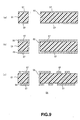
- the copper plating was performed at a current density of 2.5A/dm 2 for 20 minutes by using copper sulfate plating solution (additive of 0.2ml/L-CC-1220 available from Japan Energy Corporation) and then was washed with water and dried. Through these steps, the copper plated layer 53 was formed and the through holes 52 were made to be conductive, as shown in FIG. 9(b).
- the dry film resist (SPG-152 available from Asahi Chemical Industry Co., Ltd.) was laminated on each side of the copper plated layer at 110°C. Then, after the film mask was put in close contact with the dry film resist, it was irradiated with ultraviolet of 120mJ/cm 2 from the extra-high pressure mercury vapor lamp. Thereafter, it was treated by 10g/L-sodium carbonate of 30°C being sprayed over it at a pressure of 0.1MPa for 20 seconds and then was washed with water. Through these steps, the dry film resist was formed in an identical circuit pattern to an intended circuit pattern.
- SPG-152 available from Asahi Chemical Industry Co., Ltd.
- the double-sided substrates of the Examples 1-6 and Comparative Example 1 are about 120mm long and about 100mm wide in size and all of them have the same circuit patterns formed thereon.
- the thickness of the double-sided substrate of Comparative Example 1 was about 152 ⁇ m, whereas those of the double-sided substrates of Examples 1, 2, 3, 4, 5 and 6 were about 64 ⁇ m, 53 ⁇ m, 64 ⁇ m, 64 ⁇ m, 52 ⁇ m and 53 ⁇ m respectively, so that the thickness of the double-sided substrate of these Examples reduced 50% or more over that of Comparative Example 1.
- a demanded light-weight and low-profile multilayer printed wiring board can be produced when the double-sided substrate produced by the multilayer printed wiring board producing method of the present invention is used as the core substrate and the printed wiring(s) is/are layered on each side of the core substrate in the laminate-en-bloc method or in the build-up method.
- the electrical connection between the circuit patterns formed on opposite sides of the double-sided substrate is provided through the through holes 52 of about 150 ⁇ m in diameter, whereas in the double-sided substrates of Examples 1-6, the electrical connection therebetween is provided through the via holes of about 50 ⁇ m in diameter.
- the holes for permitting the circuit patterns formed on the opposite sides of the substrate to be conductive can be reduced in diameter. This can permit the via hole pad to reduce in diameter and thus can provide a high-density wiring.
Landscapes
- Engineering & Computer Science (AREA)
- Manufacturing & Machinery (AREA)
- Microelectronics & Electronic Packaging (AREA)
- Production Of Multi-Layered Print Wiring Board (AREA)
- Manufacturing Of Printed Circuit Boards (AREA)
Abstract
Description
| Composition of polyamic acid resin | |
| Anhydride: 3,3',4,4'- | 5 parts by weight |
| Diamine: p- | 5 parts by weight |
| Solvent: N-methyl-2- | 28 parts by weight |
Claims (4)
- A method of producing a multilayer printed wiring board comprising:a step of forming an insulating resin layer on a metal foil;a step of forming a via hole in the insulating resin layer;a step of forming a specified circuit pattern on the insulating resin layer and forming a conductive layer in the via hole, by plating; anda step of etching the metal foil to form it into the specified circuit pattern.
- The method of producing a multilayer printed wiring board according to Claim 1, wherein the metal foil is made of any of copper or copper alloy containing copper as its primary component, nickel or nickel alloy containing nickel as its primary component, alloy containing nickel and iron as its primary components, and stainless steel.
- The method of producing a multilayer printed wiring board according to Claim 1, wherein the insulating resin layer comprises polyimide.
- A multilayer printed wiring board produced in a method of producing a multilayer printed wiring board comprising:a step of forming an insulating resin layer on a metal foil;a step of forming a via hole in the insulating resin layer;a step of forming a specified circuit pattern on the insulating resin layer and forming a conductive layer in the via hole, by plating; anda step of etching the metal foil to form it into the specified circuit pattern.
Applications Claiming Priority (2)
| Application Number | Priority Date | Filing Date | Title |
|---|---|---|---|
| JP2000293895 | 2000-09-27 | ||
| JP2000293895 | 2000-09-27 |
Publications (2)
| Publication Number | Publication Date |
|---|---|
| EP1194021A2 true EP1194021A2 (en) | 2002-04-03 |
| EP1194021A3 EP1194021A3 (en) | 2003-07-23 |
Family
ID=18776602
Family Applications (1)
| Application Number | Title | Priority Date | Filing Date |
|---|---|---|---|
| EP01122596A Withdrawn EP1194021A3 (en) | 2000-09-27 | 2001-09-26 | Method of producing multilayer printed wiring board and multilayer printed wiring board |
Country Status (3)
| Country | Link |
|---|---|
| US (1) | US6772515B2 (en) |
| EP (1) | EP1194021A3 (en) |
| CN (1) | CN1229007C (en) |
Cited By (3)
| Publication number | Priority date | Publication date | Assignee | Title |
|---|---|---|---|---|
| DE102005007405A1 (en) * | 2004-11-15 | 2006-05-24 | Samsung Electro-Mechanics Co., Ltd., Suwon | Method for producing high-density printed circuit boards |
| CN101355853B (en) * | 2007-07-24 | 2012-03-28 | 日东电工株式会社 | Producing method of wired circuit board |
| EP3039948A4 (en) * | 2013-08-30 | 2017-07-12 | Elcoflex OY | Method for manufacturing a flexible circuit board and a flexible circuit board |
Families Citing this family (29)
| Publication number | Priority date | Publication date | Assignee | Title |
|---|---|---|---|---|
| US7005179B2 (en) * | 2002-07-26 | 2006-02-28 | The Regents Of The University Of California | Conductive inks for metalization in integrated polymer microsystems |
| TW587322B (en) * | 2002-12-31 | 2004-05-11 | Phoenix Prec Technology Corp | Substrate with stacked via and fine circuit thereon, and method for fabricating the same |
| JP3655915B2 (en) * | 2003-09-08 | 2005-06-02 | Fcm株式会社 | Conductive sheet and product containing the same |
| JP2005072168A (en) * | 2003-08-22 | 2005-03-17 | Nitto Denko Corp | Double-sided wiring circuit board and manufacturing method thereof |
| JP4541763B2 (en) * | 2004-01-19 | 2010-09-08 | 新光電気工業株式会社 | Circuit board manufacturing method |
| US7105372B2 (en) * | 2004-01-20 | 2006-09-12 | Headway Technologies, Inc. | Magnetic tunneling junction film structure with process determined in-plane magnetic anisotropy |
| JP4298597B2 (en) * | 2004-07-01 | 2009-07-22 | 日東電工株式会社 | Wiring circuit board and method for manufacturing wiring circuit board |
| US7703201B2 (en) * | 2004-10-25 | 2010-04-27 | International Business Machines Corporation | Method of embedding tamper proof layers and discrete components into printed circuit board stack-up |
| DE102004056259A1 (en) * | 2004-11-22 | 2006-05-24 | Rohde & Schwarz Gmbh & Co. Kg | Coupling lines for a YIG filter or YIG oscillator and method for producing the coupling lines |
| CN100386006C (en) * | 2005-02-04 | 2008-04-30 | 光宝科技股份有限公司 | Printed circuit board and method of forming the same |
| US7877866B1 (en) | 2005-10-26 | 2011-02-01 | Second Sight Medical Products, Inc. | Flexible circuit electrode array and method of manufacturing the same |
| KR20100065689A (en) * | 2008-12-08 | 2010-06-17 | 삼성전기주식회사 | A printed circuit board comprising a metal bump and a method of manufacturing the same |
| US8786062B2 (en) | 2009-10-14 | 2014-07-22 | Advanced Semiconductor Engineering, Inc. | Semiconductor package and process for fabricating same |
| US20110084372A1 (en) * | 2009-10-14 | 2011-04-14 | Advanced Semiconductor Engineering, Inc. | Package carrier, semiconductor package, and process for fabricating same |
| US8569894B2 (en) | 2010-01-13 | 2013-10-29 | Advanced Semiconductor Engineering, Inc. | Semiconductor package with single sided substrate design and manufacturing methods thereof |
| TWI411075B (en) | 2010-03-22 | 2013-10-01 | 日月光半導體製造股份有限公司 | Semiconductor package and method of manufacturing same |
| US8941222B2 (en) | 2010-11-11 | 2015-01-27 | Advanced Semiconductor Engineering Inc. | Wafer level semiconductor package and manufacturing methods thereof |
| US9406658B2 (en) | 2010-12-17 | 2016-08-02 | Advanced Semiconductor Engineering, Inc. | Embedded component device and manufacturing methods thereof |
| JP5762137B2 (en) * | 2011-05-27 | 2015-08-12 | 上村工業株式会社 | Plating method |
| US8564909B1 (en) | 2011-10-24 | 2013-10-22 | Magnecomp Corporation | Multilayer bond pads for hard disk drive suspensions |
| KR20140047480A (en) * | 2012-10-12 | 2014-04-22 | 주식회사 잉크테크 | Method for manufacturing pcb forming circuit pattern and connecting the circuit pattern through via-hole by printing method |
| JP2014086651A (en) * | 2012-10-26 | 2014-05-12 | Ibiden Co Ltd | Printed wiring board and manufacturing method for printed wiring board |
| KR102356809B1 (en) * | 2014-12-26 | 2022-01-28 | 삼성전기주식회사 | Printed circuit board and method of manufacturing the same |
| EP3412121A4 (en) * | 2016-02-01 | 2020-01-22 | Elcoflex OY | METHOD FOR MANUFACTURING AN EXTREMELY THIN FLEXIBLE MULTILAYER PRINTED CIRCUIT BOARD, AND FLEXIBLE MULTILAYER PRINTED CIRCUIT BOARD |
| CN107404798A (en) * | 2016-05-20 | 2017-11-28 | 株洲中车时代电气股份有限公司 | A kind of multilayer circuit connecting plate and its manufacture method |
| JP2020068339A (en) * | 2018-10-26 | 2020-04-30 | カンタツ株式会社 | Multilayer substrate formation method and multilayer substrate formation device |
| US10950531B2 (en) * | 2019-05-30 | 2021-03-16 | Advanced Semiconductor Engineering, Inc. | Semiconductor device package and method of manufacturing the same |
| JP6804115B1 (en) | 2019-08-09 | 2020-12-23 | 板橋精機株式会社 | Printed board |
| CN113347808B (en) * | 2021-05-13 | 2022-07-19 | 江苏普诺威电子股份有限公司 | Method for manufacturing multilayer circuit board with thick copper and ultra-fine circuit |
Family Cites Families (13)
| Publication number | Priority date | Publication date | Assignee | Title |
|---|---|---|---|---|
| US3352730A (en) | 1964-08-24 | 1967-11-14 | Sanders Associates Inc | Method of making multilayer circuit boards |
| GB1379558A (en) | 1971-05-15 | 1975-01-02 | Int Computers Ltd | Methods of manufacture of multilayer circuit structures |
| US5153987A (en) * | 1988-07-15 | 1992-10-13 | Hitachi Chemical Company, Ltd. | Process for producing printed wiring boards |
| US5153986A (en) * | 1991-07-17 | 1992-10-13 | International Business Machines | Method for fabricating metal core layers for a multi-layer circuit board |
| JPH05291727A (en) * | 1992-04-14 | 1993-11-05 | Hitachi Chem Co Ltd | Wiring board manufacturing method |
| DE59309575D1 (en) * | 1992-06-15 | 1999-06-17 | Heinze Dyconex Patente | METHOD FOR PRODUCING CIRCUIT BOARDS USING A SEMI-FINISHED PRODUCT WITH EXTREMELY TIGHT WIRING FOR THE SIGNALING |
| JPH06132630A (en) * | 1992-10-20 | 1994-05-13 | Matsushita Electric Ind Co Ltd | Flexible wiring board manufacturing method |
| WO1995002312A1 (en) * | 1993-07-07 | 1995-01-19 | Dyconex Patente Ag | Structured printed circuit boards and films and process for producing them |
| JPH07273466A (en) * | 1994-03-29 | 1995-10-20 | Hitachi Chem Co Ltd | Method for manufacturing multilayer wiring board |
| US5495665A (en) | 1994-11-04 | 1996-03-05 | International Business Machines Corporation | Process for providing a landless via connection |
| EP0744884A3 (en) * | 1995-05-23 | 1997-09-24 | Hitachi Chemical Co Ltd | Process for producing multilayer printed circuit board |
| JP2751902B2 (en) * | 1995-12-27 | 1998-05-18 | 日本電気株式会社 | Method for manufacturing multilayer printed wiring board |
| SG109405A1 (en) | 1999-02-04 | 2005-03-30 | Gul Technologies Singapore Ltd | Printed circuit boards with solid interconnect and method of producing the same |
-
2001
- 2001-09-25 US US09/960,919 patent/US6772515B2/en not_active Expired - Fee Related
- 2001-09-26 EP EP01122596A patent/EP1194021A3/en not_active Withdrawn
- 2001-09-27 CN CN01141148.1A patent/CN1229007C/en not_active Expired - Fee Related
Cited By (3)
| Publication number | Priority date | Publication date | Assignee | Title |
|---|---|---|---|---|
| DE102005007405A1 (en) * | 2004-11-15 | 2006-05-24 | Samsung Electro-Mechanics Co., Ltd., Suwon | Method for producing high-density printed circuit boards |
| CN101355853B (en) * | 2007-07-24 | 2012-03-28 | 日东电工株式会社 | Producing method of wired circuit board |
| EP3039948A4 (en) * | 2013-08-30 | 2017-07-12 | Elcoflex OY | Method for manufacturing a flexible circuit board and a flexible circuit board |
Also Published As
| Publication number | Publication date |
|---|---|
| CN1229007C (en) | 2005-11-23 |
| EP1194021A3 (en) | 2003-07-23 |
| US20020056192A1 (en) | 2002-05-16 |
| CN1347277A (en) | 2002-05-01 |
| US6772515B2 (en) | 2004-08-10 |
Similar Documents
| Publication | Publication Date | Title |
|---|---|---|
| US6772515B2 (en) | Method of producing multilayer printed wiring board | |
| US7918021B2 (en) | Production of via hole in a flexible printed circuit board by applying a laser or punch | |
| CN1333623C (en) | Method for producing vias in manufacture of printed wiring boards | |
| US6107003A (en) | Method for producing multi-layer printed wiring boards having blind vias | |
| JPH06318783A (en) | Method for manufacturing multilayer circuit board | |
| JPH06275950A (en) | Manufacture of wiring board | |
| JPH1187865A (en) | Printed wiring board and method of manufacturing the same | |
| US6884944B1 (en) | Multi-layer printed wiring boards having blind vias | |
| JPH11214846A (en) | Multilayer printed wiring board | |
| JP2002176259A (en) | Method of manufacturing multilayer printed wiring board and multilayer printed wiring board | |
| JP3500977B2 (en) | Manufacturing method of double-sided circuit board | |
| JPH098458A (en) | Printed wiring board and manufacturing method thereof | |
| JP4011968B2 (en) | Wiring board, manufacturing method thereof, and conductor tension plate | |
| JP2000340948A (en) | Method for improving adhesion between copper and resin and multilayer wiring board manufactured using the same | |
| JP3373406B2 (en) | Printed wiring board and method of manufacturing the same | |
| JP2003273509A (en) | Wiring board and method of manufacturing the same | |
| JP2001015919A (en) | Circuit board for multilayer printed wiring board, method for manufacturing the same, and multilayer printed wiring board | |
| JP3559598B2 (en) | Metal foil for printed wiring board, method for manufacturing the same, and method for manufacturing wiring board using the metal foil | |
| JP2004273744A (en) | Thermoplastic resin material and method for manufacturing printed wiring board | |
| WO2003032701A1 (en) | Method for manufacturing multilayer wiring board, and multilayer wiring board manufactured by the same | |
| JP2000036662A (en) | Method for manufacturing build-up multilayer wiring board | |
| JP2003243810A (en) | A method for manufacturing a printed wiring board having an ultrafine line pattern. | |
| JP2002314247A (en) | Multilayer printed wiring board and method of manufacturing the same | |
| JPH1168291A (en) | Printed wiring board and manufacturing method thereof | |
| EP0848585A1 (en) | Process for the manufacture of printed circuit boards with plated resistors |
Legal Events
| Date | Code | Title | Description |
|---|---|---|---|
| PUAI | Public reference made under article 153(3) epc to a published international application that has entered the european phase |
Free format text: ORIGINAL CODE: 0009012 |
|
| AK | Designated contracting states |
Kind code of ref document: A2 Designated state(s): AT BE CH CY DE DK ES FI FR GB GR IE IT LI LU MC NL PT SE TR |
|
| AX | Request for extension of the european patent |
Free format text: AL;LT;LV;MK;RO;SI |
|
| PUAL | Search report despatched |
Free format text: ORIGINAL CODE: 0009013 |
|
| AK | Designated contracting states |
Designated state(s): AT BE CH CY DE DK ES FI FR GB GR IE IT LI LU MC NL PT SE TR |
|
| AX | Request for extension of the european patent |
Extension state: AL LT LV MK RO SI |
|
| 17P | Request for examination filed |
Effective date: 20031029 |
|
| AKX | Designation fees paid |
Designated state(s): BE DE FI FR GB |
|
| RAP1 | Party data changed (applicant data changed or rights of an application transferred) |
Owner name: NITTO DENKO CORPORATION |
|
| 17Q | First examination report despatched |
Effective date: 20070305 |
|
| STAA | Information on the status of an ep patent application or granted ep patent |
Free format text: STATUS: THE APPLICATION IS DEEMED TO BE WITHDRAWN |
|
| 18D | Application deemed to be withdrawn |
Effective date: 20090911 |