Technical Field
The present invention relates to an optical filter
comprising a filter layer absorbing visible light, a
transparent support, in particular a transparent support
comprising a biaxially stretched film, and an
antireflection layer. In particular, the present invention
relates to an optical filter attached to the display of
image displays, e.g., a liquid crystal display (LCD), a
plasma display panel (PDP), an electroluminescence display
(ELD), a cathode ray tube (CRT), a fluorescent character
display tube and an electric field emission display for the
purpose of preventing reflection and improving color
reproduction. The present invention further relates to the
front panel of a plasma display panel (PDP) and the body of
PDP equipped with an optical filter for preventing
reflection and improving color reproduction.
Background Art
Various kinds of image displays, e.g., a liquid
crystal display (LCD), a plasma display panel (PDP), an
electroluminescence display (ELD), a cathode ray tube (CRT),
a fluorescent character display tube and an electric field
emission display, have been developed and apparatuses
incorporated these image displays have been put to
practical use in recent years.
These image displays are confronted with various
problems, e.g., a problem that color correction is necessary
since color purity and color separation of display
elements are insufficient, a problem that contrast is
reduced since backgrounds are reflected on displays, and a
problem of leaking out of infrared rays and electromagnetic
waves attributable to display elements. For coping with
each problem, it is proposed to use a visible filter for
color correction, an antireflection film, an infrared ray-shielding
filter, and an electromagnetic wave-shielding
filter, etc., on the front of displays.
In particular, color correction by a filter is
described in Japanese Patent Laid-Open Nos. 153904/1983,
188501/1986, 231988/1991, 205643/1993, 145918/1997,
306366/1997 and 26704/1998 and WO98/23980.
Various kinds of producing methods of optical
filters are disclosed. In the optical filters disclosed in
Japanese Patent Laid-Open Nos. 188501/1986, 205643/1993,
145918/1997 and 306366/1997, dyes or pigments are added to
transparent supports to make the supports function as
filters. In the optical filter disclosed in Japanese
Patent Laid-Open No. 26704/1998, the hard coat layer (the
surface-hardening layer) provided between the transparent
support and the antireflection layer is colored to make the
hard coat layer function as a filter. In the optical
filter disclosed in Japanese Patent Laid-Open No.
209510/1995, a mixed solution of a dye and a metal alkoxide
are coated, dried and burned to make it function as the
filter layer. Further, in the optical filter disclosed in
WO98/23980, a dye and a matrix polymer is dissolved in an
appropriate solvent and coated to make it function as the
filter layer.
However, the filter layers produced by these
methods come to reflect light of specified wavelength when
the concentration of the dyes in the filter layers becomes
high, which deteriorates color correcting performance of
the optical filter. Contrary to this, when the dye
concentration in a filter layer is lowered, the thickness
of the filter layer should be increased to obtain the
optical concentration as the optical filter. Accordingly,
in the production process of filter layers by coating,
troubles such as drying failure and cracking of films are
liable to occur.
Further, multilayer antireflection films produced
by laminating transparent thin films of metal oxides, which
are used for spectacle lenses, camera lenses, etc., are
used for preventing reflection, and the more the layer
number, the more effective is the multilayer antireflection
film to the lights of a wide wavelength range. Therefore,
multilayer lamination of transparent thin films by a vacuum
deposition method, a sputtering method, an ion-plating
method, a CVD method, or a PVD method has been performed.
However, since a high degree of vacuum is necessary
in these methods, equipment becomes large-scaled, further
it is required to exactly control the thickness of each
layer according to the relationship between the refractive
indices and the film thicknesses previously designed,
therefore, there is a problem in the productivity and it is
difficult to produce an antireflection film on a large size
film inexpensively.
Further, since films are deformed and denatured by
heat, they cannot be exposed to a high temperature, in
addition the volatile components (water, solvents, etc.) of
films hinder maintaining a high degree of vacuum, so there
arises a problem that the film thickness and strength are
liable to become uneven when transparent thin films each
having a different refractive index are laminated on a film
by a vacuum deposition method or a sputtering method.
For solving such problems due to a vacuum
deposition or sputtering method, a method of forming an
antireflection film by wet coating has been discussed. For
example, an antireflection transparent material containing
microvoids and an inorganic fine particles of a diameter of
from 1 to 300 nm and having an antireflection layer having
a refractive index lower than that of the substrate is
disclosed in Japanese Patent Laid-Open No. 59250/1985.
However, even with to this technique, the obtained sample
must be subjected to treatment with an activated gas under
vacuum to lower the refractive index, which encounters the
same problem as the deposition (high vacuum system and
delicate control of activated gas treatment).
Further, in Japanese Patent Laid-Open Nos.
49501/1984, 50401/1984 and 48527/1995, antireflection films
having a low refractive index layer using silica particles
and a silane hydrolyzed product as the binder are disclosed.
However, in this constitution, it is difficult to suppress
the refractive index of the low refractive index layer
sufficiently low, thus such a problem as a low refractive
index cannot be obtained still remains.
A variety of subjects are required of these filters
respectively by the kinds of displays, e.g., a visible
filter for color correction is required to form a sharp
absorber corresponding to the characteristics of the
display elements, in addition, strengthening of a heat
resisting property by glass incorporation, etc., and
physical strengthening are required. Further, it is
necessary for an antireflection film to have multilayer
structure for achieving ideal refractive indices in every
range of visible light, however, forming a multilayer film
by deposition or coating is accompanied by processing
difficulties and an economical problem. Accordingly, when
various functions are tried to be given to the front panel
of a display, there arises the restriction that one
function must not hinder other functions in addition to the
fact that filters having the respective functions are
required to have respective characteristics. Therefore, a
multifunctional front panel has not been put to practical
use as yet.
Further, the front panel having an antireflection
layer and a selectively absorptive filter layer is required
to have strength of more than a certain degree since not
only the front panel must prevent the scattering of display
elements at the back of the front panel at the time of
breakage but also it has to be sufficiently resistive to
the breakage of its own.
Accordingly, an object of the present invention is
to provide a multifunctional optical filter which satisfies
the requirements such as excellence in production aptitude,
non-bulk, light weight and high mechanical strength, and a
front panel and an image display using the same, in
particular, to provide an optical filter having a proper
color correcting performance in addition to the
antireflection performance, and a front panel and an image
display using the same.
Another object of the present invention is to
provide an optical filter capable of selectively cutting
the light of the wavelengths which reduce color purity to
correct color balance, and to provide an image display
using the same.
A further object of the present invention is to
provide an optical filter which can suppress the reduction
of visibility due to the reflection of external light on a
display panel, can regulate colors and is improved in
resistance to breakage.
Disclosure of the Invention
The above objects of the present invention have
been accomplished by the following invention.
Brief Description of the Drawings
Fig. 1 is a cross-sectional conceptual drawing in
the case of using the front panel of the present invention
at the front of body A of a cathode ray tube (CRT) or a
plasma display panel (PDP).
Fig. 1 (a) is a conceptual drawing of the case
where body A is in contact with front panel D, and Fig. 1
(b) is a conceptual drawing of the case where there is a
space between body A and front panel D.
- A
- CRT or PDP
- B
- Biaxially stretched transparent support
- C
- Optical filter (various kinds of filter layers and
antireflection layers)
- D
- Front panel
- E
- The face of the observation side of a front panel
- F
- The face of the CRT or PDP side of a front panel
- G
- The face of the observation side of CRT or PDP
Fig. 2 is a cross-sectional typical drawing of the
layer constitution of a front panel. Fig. 2 (a) and Fig. 2
(b) are the examples of the layer constitutions
corresponding to the arrangement of Fig. 1 (a), and Fig. 2
(c) and Fig. 2 (d) are those to the arrangement of Fig. 1
(b).
- 1
- Antireflection layer
- 2
- Eelectromagnetic wave- and infrared ray-shielding layer
- 3
- Hard coat layer
- 4
- Biaxially stretched transparent support
- 5
- Filter layer
- 6
- Transparent glass support
Best Mode for Carrying out the Invention
The present invention can be explained with
referring to some examples shown below, but the present
invention is not limited thereto unless otherwise indicated.
A plasma display panel (PDP) in the present
invention comprises a gas, a glass substrate, an electrode,
an electrode lead material, a thick print material and a
fluorescent material. The glass substrate consists of a
front glass substrate and a rear glass substrate.
Electrodes and insulating layers are formed on the two
glass substrates. A fluorescent material layer is further
formed on the rear glass substrate. The two glass
substrates are assembled and a gas is sealed therebetween.
The front panel is a substrate which is positioned
in front of the plasma display panel. It is preferred that
the front panel possesses sufficient strength for
protecting the plasma display panel. The front panel may
be used with leaving space between the front panel and the
plasma display panel or may be directly adhered to the
plasma display body.
The plasma display in the present invention means
the entire display comprising at least the plasma display
panel body and the box. When the plasma display has a
front panel, it is also included in the plasma display.
The plasma display panel (PDP) has come into the
market. The plasma display panel is disclosed in Japanese
Patent Laid-Open Nos. 205643/1993 and 306366/1997.
The representative layer constitutions of the
optical filter for the image display and the front panel
using the same in the present invention are explained with
referring to the accompanying drawings.
The layer constitutions of the optical filter used
as the front panels of or the parts of the cathode ray tube
(CRT) and the plasma display panel (PDP) are described
below.
Fig. 1 is a cross-sectional conceptual drawing in
the case of using front panel D of the present invention at
the front of body A of a cathode ray tube (CRT) or a plasma
display panel (PDP). Fig. 1 (a) is a conceptual drawing of
the case where body A is in contact with front panel D, and
optical filter C comprising various kinds of filter layers
and antireflection layers is provided only on one side (the
front) of the support of the front panel. Fig. 1 (b) is a
conceptual drawing of the case where there is a space
between body A and front panel D, and optical filter C
comprising various kinds of filter layers and
antireflection layers are provided on both sides of the
support of the front panel.
Fig. 2 is a cross-sectional typical drawing of the
layer constitution of the optical filter and a front panel
using the same. Fig. 2 (a) and Fig. 2 (b) are the examples
of the layer constitutions of the optical filters
corresponding to the arrangement of Fig. 1 (a) and the
front panels using the same, and Fig. 2 (c) and Fig. 2 (d)
are the examples of the layer constitutions of the optical
filters corresponding to the arrangement of Fig. 1 (b) and
the front panels using the same.
In Fig. 2 (a), it is preferred that undercoat
layers are provided between the biaxially stretched.
transparent support and the hard coat layer and between the
biaxially stretched transparent support and the filter
layer for obtaining sufficient adhesion strength.
In Fig. 2 (b), it is preferred that an undercoat
layer is provided between the biaxially stretched
transparent support and the filter layer for obtaining
sufficient adhesion strength. The filter layer and the
transparent glass support can be easily adhered by means of,
e.g., commercially available acrylic-based adhesives.
In Fig. 2 (c) and Fig. 2 (d), it is preferred that
undercoat layers are provided between the biaxially
stretched transparent support and the filter layer and
between the biaxially stretched transparent support and the
antireflection layer for obtaining sufficient adhesion
strength.
(Transparent support)
The transparent support for use in the present
invention is described in detail below. The examples of
the transparent supports which can be used in the present
invention include cellulose ester (e.g., diacetyl cellulose,
triacetyl cellulose (TAC), propionyl cellulose, butyryl
cellulose, acetyl propionyl cellulose, nitrocellulose),
polyamide, polycarbonate, polyester (e.g., polyethylene
terephthalate, polyethylene naphthalate, polybutylene
terephthalate, poly-1,4-cyclohexanedimethylene
terephthalate, polyethylene-1,2-diphenoxyethane-4,4'-dicarboxylate),
polyallylate (e.g., condensation products
of bisphenol A and phthalic acid), polystyrene (e.g.,
syndiotactic polystyrene), polyolefin (e.g., polyethylene,
polypropylene, polymethylpentene), acryl(polymethyl
methacrylate), polysulfone, polyether sulfone, polyether
ketone, polyether imide and polyoxyethylene. Triacetyl
cellulose, polycarbonate, polymethyl methacrylate,
polyethylene terephthalate and polyethylene naphthalate are
preferred.
The transparent support preferably has a thickness
of from 5 µm to 5 cm, more preferably from 25 µm to 1 cm,
and most preferably from 80 µm to 1.2 mm.
It is preferred to use a biaxially stretched film
as the transparent support.
Examples of the materials of the biaxially
stretched films include polyester (e.g., polyethylene
terephthalate, polyethylene naphthalate, polybutylene
terephthalate, poly-1,4-cyclohexanedimethylene
terephthalate, polyethylene-1,2-diphenoxyethane-4,4'-dicarboxylate,
polybutylene terephthalate), polyamide,
polycarbonate, polyallylate (e.g., condensation products of
bisphenol A and phthalic acid), polystyrene (e.g.,
syndiotactic polystyrene), polyphenylene sulfide, polyether
ether ketone, polyolefin (e.g., polyethylene, polypropylene,
polymethylpentene), polysulfone, polyether sulfone, and
polyoxyethylene. Polyester, polycarbonate and polyallylate
(e.g., condensation products of bisphenol A and phthalic
acid) are preferred, and from the viewpoint of mechanical
strength, durability, wide usage and heat resistance,
polyester, in particular, polyesters containing ethylene
terephthalate and ethylene-2,6-naphthalate as main
repeating units are preferred. In the present invention,
polyethylene terephthalate is a polymer containing an
ethylene terephthalate unit as a main repeating unit.
Further, in the present invention, polyethylene naphthalate
is a polymer containing an ethylene-2,6-naphthalate unit as
a main repeating unit. "Containing as a main repeating
unit" used herein means that it is a polymer containing the
repeating unit in an amount of 70 mol% or more, preferably
85 mol% or more, and more preferably 95 mol% or more, and
copolymerizable other components, glycol components other
than ethylene glycol, dicarboxylic acid components other
than terephthalic acid or 2,6-naphthalenedicarboxylic acid,
or a small amount of trifunctional components may be
contained.
The biaxially stretched transparent support is a
film obtained by melt-extruding resin compositions
comprising any of the above resin as a main component,
biaxially stretching and thermally fixing.
The biaxially stretched transparent support has a
thickness of from 10 to 500 µm, preferably from 20 to 300
µm, and more preferably from 50 to 200 µm.
The biaxially stretched transparent support
according to the present invention is large in the
transmittance of rays of the support itself and excellent
in mechanical strength and heat resistance due to the
synergistic effect of the above biaxial stretching and the
specific thickness of the support, therefore, it becomes
possible to laminate layers having various functions.
The transparent support preferably has a
transmittance of 80% or more, more preferably 86% or more.
Since when the tensile impact strength of the transparent
support is weak, if the transparent support to be used is
not thick, the impact strength of a certain degree or more
cannot be obtained, the objective transmittance may not be
obtained. Therefore, it is necessary that the tensile
impact strength be 294 kJ/m2 even at the lowest, and 392
kJ/m2 or more in practice. A tensile impact strength can
be obtained according to ASTM D1822-93.
The haze is preferably 5% or less, more preferably
4% or less.
The refractive index is preferably from 1.45 to
1.70.
An infrared absorber or an ultraviolet absorber may
be added to the transparent support. The addition amount
of an infrared absorber is preferably from 0.01 to 20 wt%,
more preferably from 0.05 to 10 wt%, of the transparent
support. Further, the particles of inactive inorganic
compounds may be added as a sliding agent to the
transparent support. The examples of inorganic compounds
include SiO2, TiO2, BaSO4, CaCO3, talc and kaolin. It is
preferred that the transparent support is subjected to
surface treatment so as to further heighten the adhesion to
the undercoat layer. As such surface treatments, chemical
treatment, mechanical treatment, corona discharge treatment,
flame treatment, ultraviolet irradiation treatment, high
frequency treatment, glow discharge treatment, active
plasma treatment, laser treatment, mixed acid treatment and
ozone oxidation treatment can be exemplified, glow
discharge treatment, ultraviolet irradiation treatment,
corona discharge treatment, and flame treatment are
preferred, and corona discharge treatment is more preferred.
(Filter layer)
It is preferred that the filter layer has an
absorption maximum in the range of wavelength of from 500
to 620 nm, more preferably absorption maximums in both of
from 500 to 550 nm and from 560 to 620 nm.
The transmittance of the range of wavelength of
from 500 to 550 nm is preferably from 20 to 85%, more
preferably from 40 to 85%.
The absorption maximum in the range of wavelength
of from 500 to 550 nm is set to adjust the emission
strength of a green fluorescent material of high visibility.
It is preferred that the emission range of a green
fluorescent material is cut gently. The half value width
(the width of the region of the wavelength showing the
absorbance of half of the absorbance at absorption maximum)
of the absorption maximum in the range of wavelength of
from 500 to 550 nm is preferably from 30 to 300 nm, more
preferably from 40 to 300 nm, still more preferably from 50
to 150 nm, and most preferably from 60 to 150 nm.
The transmittance at absorption maximum in the
range of wavelength of from 560 to 620 nm is preferably
from 0.01 to 80%, preferably from 0.01 to 60%, and
particularly preferably from 0.01 to 40%.
The absorption maximum in the range of wavelength
of from 560 to 620 nm is set to selectively cut the subband
which lowers the color purity of a red fluorescent
material. In PDP, unnecessary luminescence in the vicinity
of 585 nm emitted by the excitation of neon is cut and at
the same time lights of short wave side from red
fluorescent material is cut. By separating absorption
maximum according to the present invention, light can be
cut selectively without adversely affecting the color tone
of a green fluorescent material. For further reducing the
influence on the color tone of a green fluorescent material,
the peak of absorption spectrum is preferably sharp.
Specifically, the half value width of the absorption
maximum in the range of wavelength of from 560 to 620 nm is
preferably from 5 to 200 nm, more preferably from 10 to 100
nm, and most preferably from 10 to 50 nm.
For giving the above absorption spectrum, a filter
layer is formed by using a coloring material (a dye or a
pigment).
The weight ratio of the dye and the binder in the
filter layer in the present invention is desirably from
1:50 to 1:2,000, preferably from 1:75 to 1:1,000, and more
preferably from 1:100 to 1:500. If the dye/binder ratio is
larger than this range, the dye concentration in the filter
layer is high, hence the filter layer comes to reflect the
light of specific wavelength, which deteriorates the color
correction function of the optical filter. While when the
ratio is smaller than this range, the dye concentration in
the filter layer is low, hence the layer thickness of the
filter layer must be thick for obtaining desired optical
density. The production of a thick filter layer is often
accompanied by troubles such as streaks by coating, drying
failure and cracking of a film in coating and drying, or
even if the layers are divided and thin layers are
laminated, the producing process is complicated,
accordingly the manufacture is not easy.
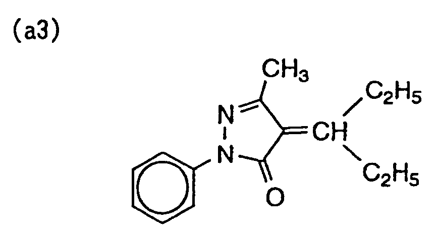
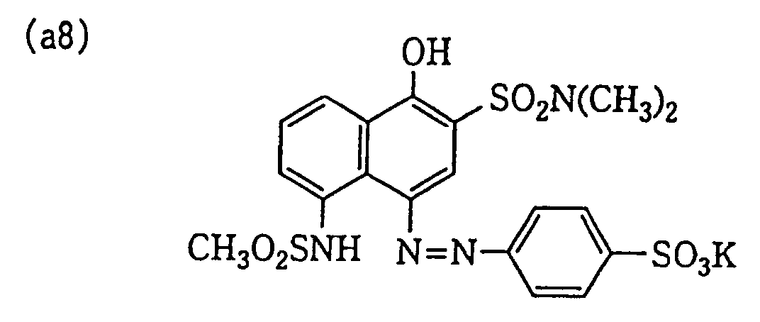
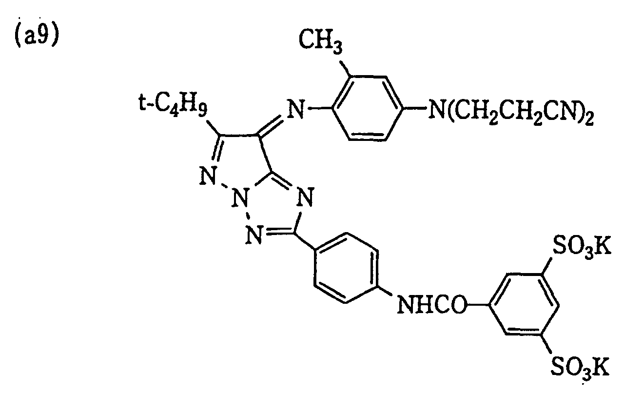
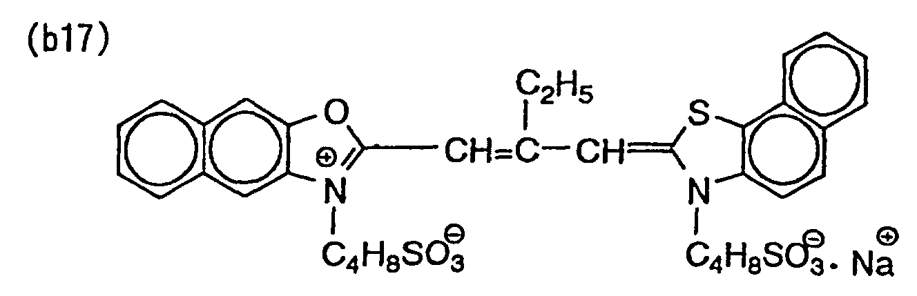
As the dyes having an absorption maximum in the
range of wavelength of from 500 to 550 nm, a squarylium-based,
azomethine-based, cyanine-based, oxonol-based,
anthraquinone-based, azo-based or benzylidene-based
compound is preferably used. Many azo dyes disclosed in
British Patents 539,703 and 575,691, U.S. Patent 2,956,879
and Hiroshi Horiguchi, Sosetsu Gosei Senryo (An
Introduction to Synthetic Dyes), Sankyo Shuppan Co., Ltd.,
etc., can be used as the azo dyes. An azo dye represented
by formula (a6) is preferred. Some examples of the dyes
having an absorption maximum in the range of wavelength of
from 500 to 550 nm are shown below.
| Compound | M | (R1)m1 | (R2)m2 | (R3)m3 |
| (a6-1) | Cu | 4-SO3Na | 8-SO3Na | 5-SO3Na |
| (a6-2) | Cu | 4-Cl, 6-SO3Na | 8-SO3Na | 5-SO3Na |
| (a6-3) | Cu | 4, 6, di-NO2 | 8-SO3Na | 5-SO3Na |
wherein R
1, R
2 and R
3 each independently represents a
hydrogen atom or a monovalent group; M represents a metal
atom; and m
1, m
2 and m
3 each independently represents an
integer of from 1 to 4. As the metal atoms represented by
M, transition metals are preferred, e.g., Fe, Co, Ni, Cu,
Zn and Cd can be exemplified, and Cu is particularly
preferred.
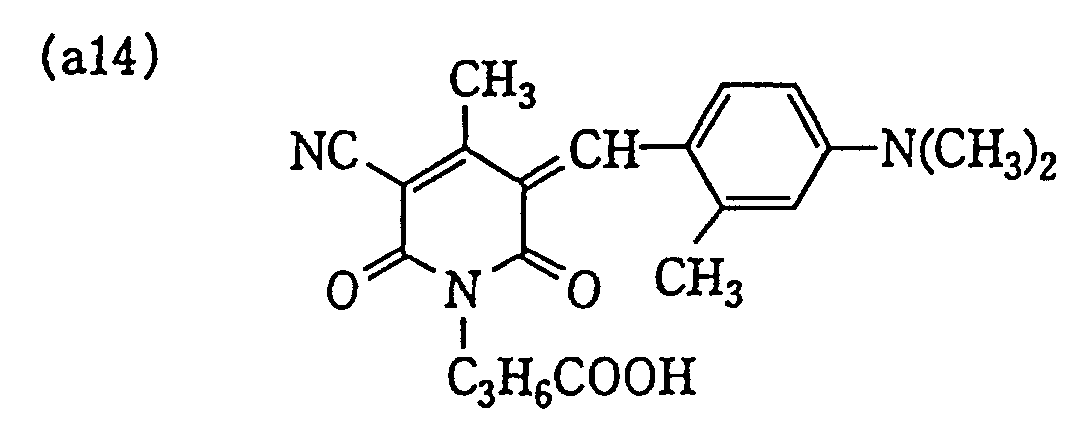
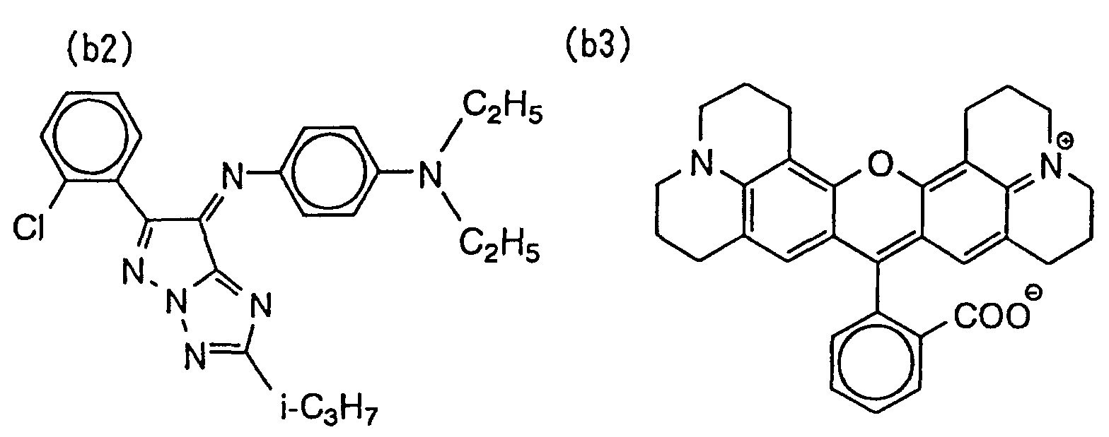
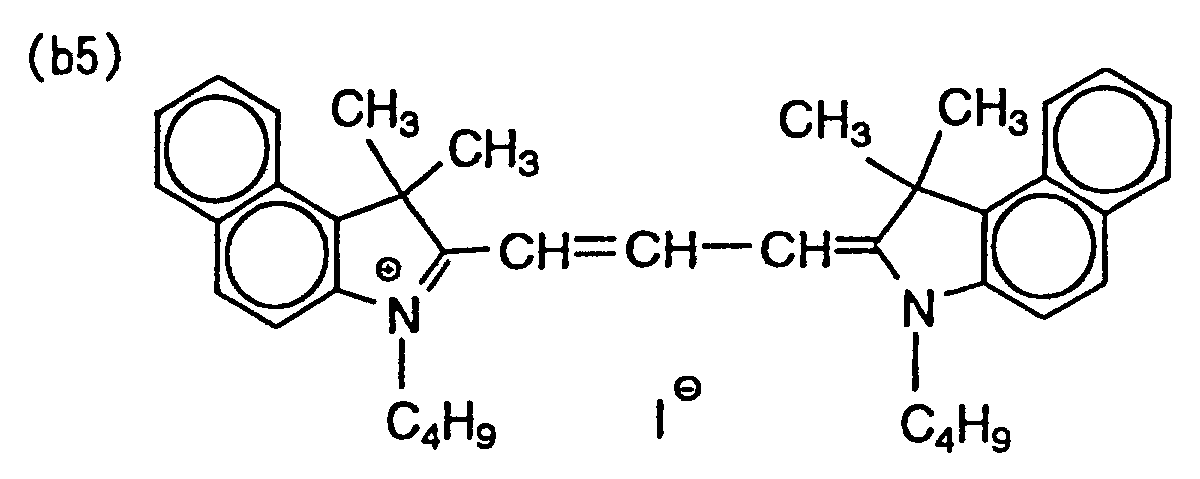
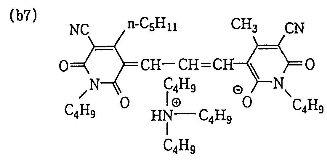
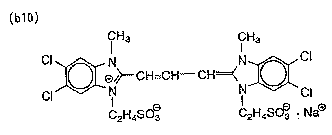
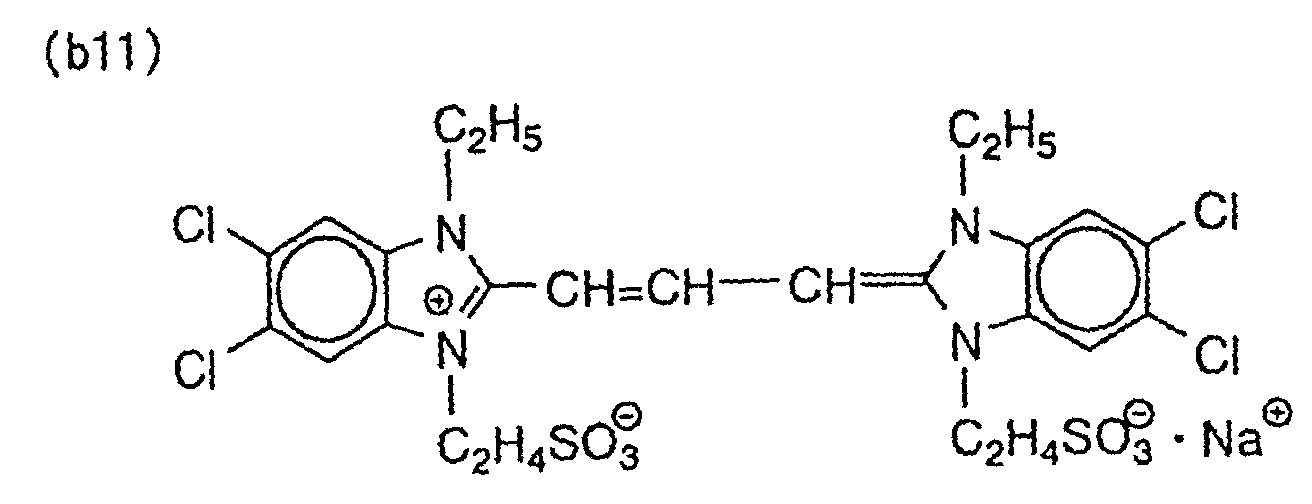
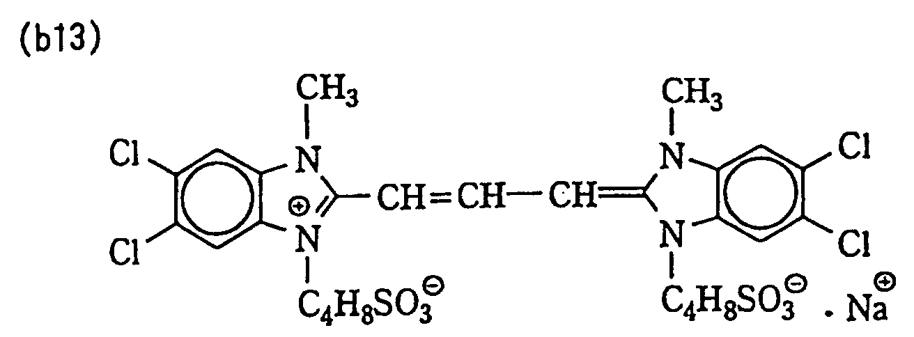
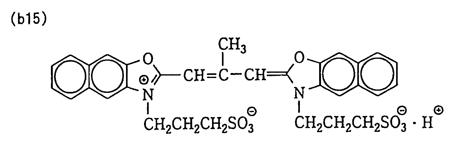
As the dyes having an absorption maximum in the
range of wavelength of from 560 to 620 nm, a cyanine-based,
squarylium-based, azomethine-based, xanthene-based, oxonol-based
or azo-based compound is preferably used. Examples
of the dyes having an absorption maximum in the wavelength
range of from 560 to 620 nm are shown below.
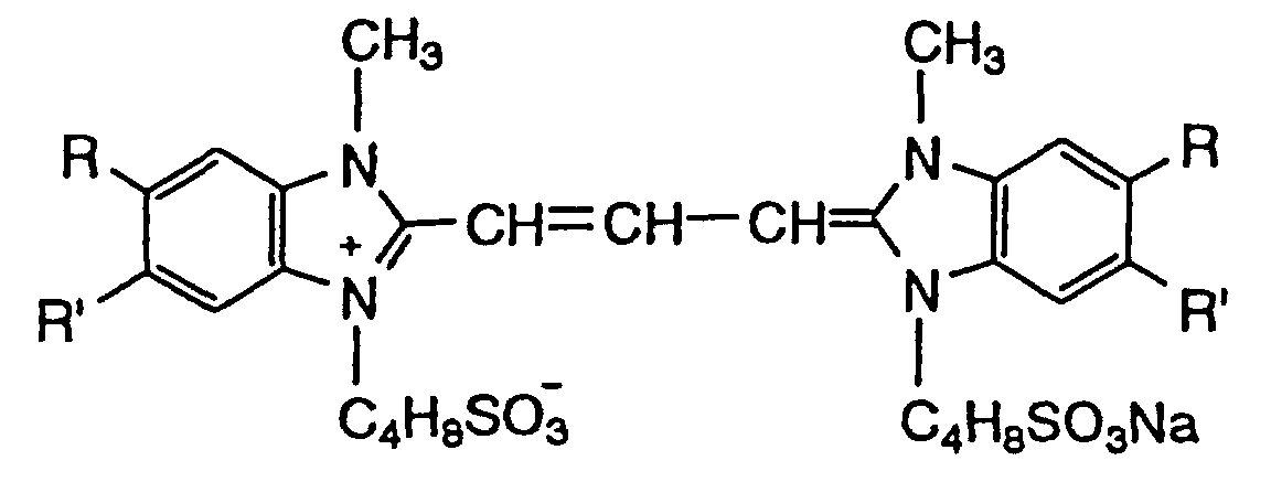
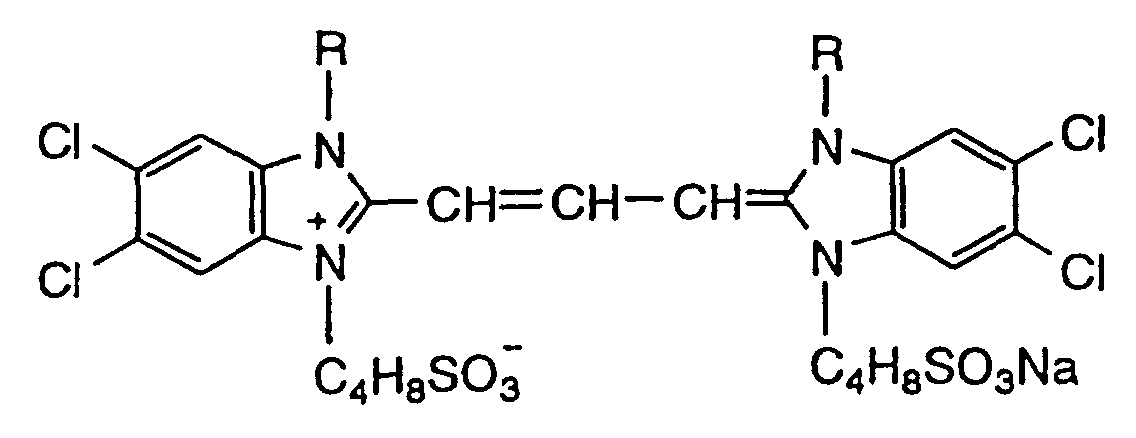
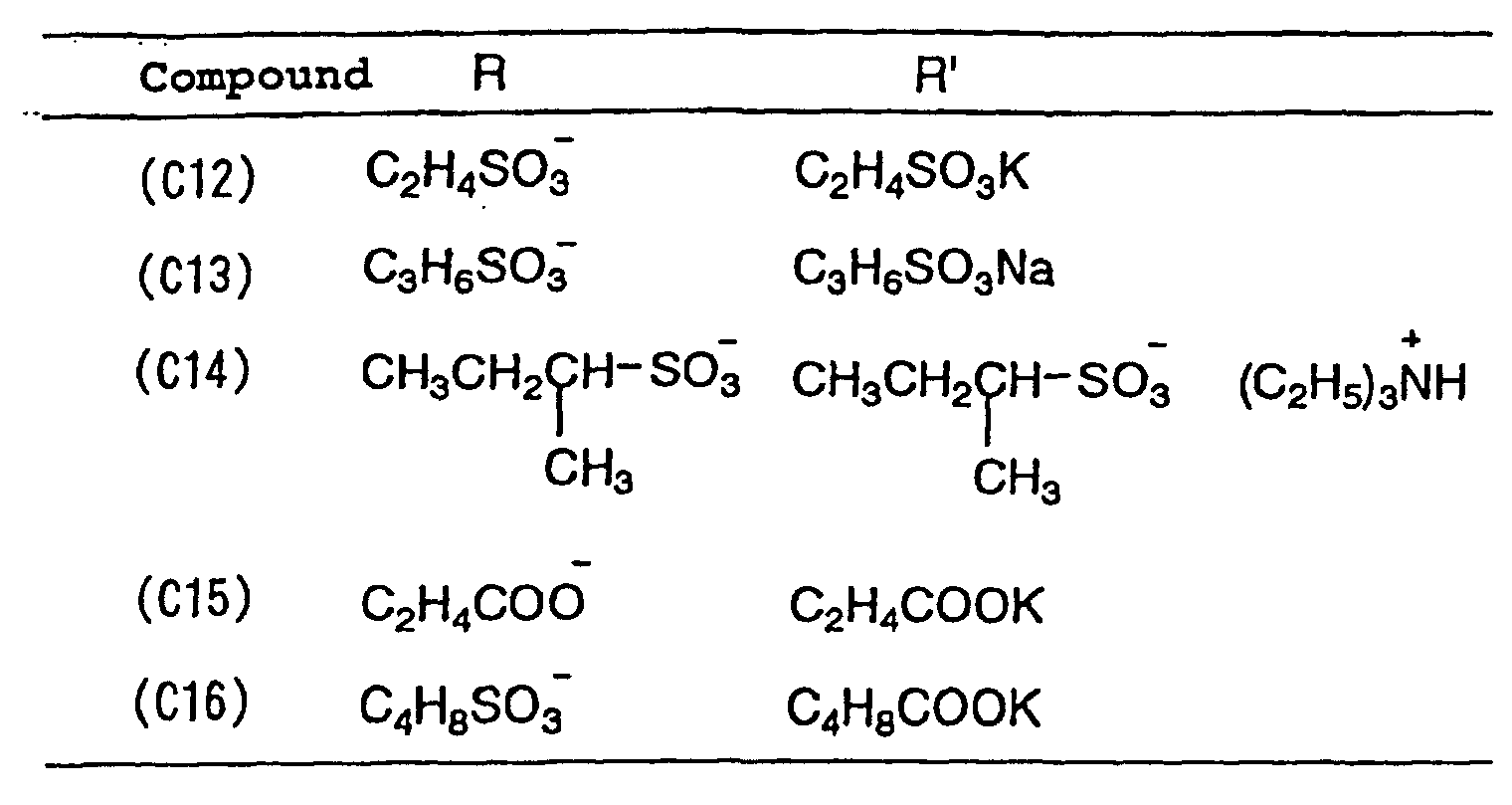
The dyes having absorption maximums in both
wavelength ranges of from 500 to 550 nm and from 560 to 620
nm can be used in a filter layer. For instance, when a dye
is in the state of aggregates such as a fine particle
dispersion, the wavelength generally shifts to longer
wavelength side and the peak becomes sharp. Accordingly,
the aggregates of some of the dyes having an absorption
maximum in the wavelength range of from 500 to 550 nm have
an absorption maximum in the wavelength range of from 560
to 620 nm. By using such a dye in the state of partially
forming aggregates, absorption maximums can be obtained in
both ranges of wavelengths of from 500 to 550 nm and from
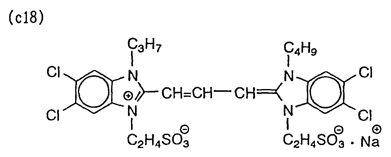
560 to 620 nm. Some examples of such dyes are shown below.
| Compound | R | R' |
| (C1) | Cl | Cl |
| (C2) | Cl | CF3 |
| (C3) | H | Cl |
| (C4) | H | CF3 |
| (C5) | H | COOH |
| (C6) | H | CONH2 |
| Compound | R |
| (C7) | C2H5 |
| (C8) | n-C3H7 |
| (C9) | t-C3H7 |
| (C10) | C2H4OCH3 |
| (C11) | C2H4OH |
Two kinds or more dyes can be used in combination
in a filter layer as described above.
A filter layer further comprises a polymer binder.
Natural polymers (e.g., gelatin, cellulose derivatives,
alginic acid) or synthetic polymers (e.g., polymethyl
methacrylate, polyvinyl butyral, polyvinyl pyrrolidone,
polyvinyl alcohol, polyvinyl chloride, styrene-butadiene
copolymer, polystyrene, polycarbonate, water-soluble
polyamide) can be used as the binder polymer. Hydrophilic
polymers (e.g., the above-described natural polymers,
polyvinyl butyral, polyvinyl pyrrolidone, polyvinyl alcohol
and water-soluble polyamide) are particularly preferably
used.
The thickness of a filter layer is preferably from
0.1 µm to 5 cm, more preferably from 0.5 µm to 1 cm, and
most preferably from 1 µm to 7 mm.
(Undercoat layer)
When the above-described filter layer, infrared
ray-shielding layer and electromagnetic wave-shielding
layer are provided on a support, an undercoat layer can be
provided on the support. As the undercoat layer, soft
polymers having a modulus of elasticity at room temperature
of from 1 to 1,000 MPa, preferably from 5 to 800 MPa, more
preferably from 10 to 500 MPa, are preferably used. The
thickness of the undercoat layer is preferably from 2 nm to
20 µm, more preferably from 5 mn to 5 µm, and most
preferably from 50 nm to 1 µm.
The polymers for use in the undercoat layer
preferably has a glass transition temperature of from -60°C
to 60°C. As the examples of the polymers having a glass
transition temperature of from -60°C to 60°C, polymers or
copolymers of vinyl chloride, vinylidene chloride, vinyl
acetate, butadiene, neoprene, styrene, chloroprene, acrylic
ester, methacrylic ester, acrylonitrile, or methyl vinyl
ether can be exemplified. A plurality of undercoat layers
can be provided, and it is preferred to provide two
undercoat layers.
(Antireflection layer)
The regular reflectance of an antireflection layer
is 3.0% or less, preferably 1.8% or less. A low refractive
index layer is usually provided as the antireflection layer.
The refractive index of the low refractive index layer is
lower than the refractive index of the above-described
transparent support. The refractive index of the low
refractive index layer is preferably from 1.20 to 1.55,
more preferably from 1.30 to 1.50. The thickness of the
low refractive index layer is preferably from 50 to 400 nm,
more preferably from 50 to 200 nm.
The low refractive index layer can be formed as a
layer comprising a low refractive index fluorine-containing
polymer (Japanese Patent Laid-Open Nos. 34526/1982,
130103/1991, 115023/1994, 313702/1996 and 168004/1995), a
layer obtained by a sol-gel method (Japanese Patent Laid-Open
Nos. 208811/1993, 299091/1994, 168003/1995), or a
layer containing fine particles (Japanese Patent
Publication No. 59250/1985, and Japanese Patent Laid-Open
Nos. 13021/1993, 56478/1994, 92306/1995 and 288201/1997).
In the layer containing fine particles, voids can be formed
in the low refractive index layer as micro voids among fine
particles or in fine particles. The layer containing fine
particles preferably has voids of from 3 to 50 vol%, more
preferably from 5 to 35 vol%.
It is preferred that a layer high in refractive
index (a middle or high refractive index layer) is
laminated on the low refractive index layer for preventing
the reflection of a broad wavelength region.
The refractive index of the high refractive index
layer is preferably from 1.65 to 2.40, more preferably from
1.70 to 2.20. The refractive index of the middle
refractive index layer is adjusted so as to be the middle
value between the refractive index of the low refractive
index layer and the refractive index of the high refractive
index layer. The refractive index of the middle refractive
index layer is preferably from 1.50 to 1.90.
The thickness of the middle/high refractive index
layers is preferably from 5 nm to 100 µm, more preferably
from 10 nm to 10 µm, and most preferably from 30 nm to 1 µm.
The haze of the middle/high refractive index layers
is preferably 5% or less, more preferably 3% or less, and
most preferably 1% or less.
The middle/high refractive index layers can be
formed by using a polymer having a relatively high
refractive index. The examples of the polymers having high
refractive index include polystyrene, styrene copolymers,
polycarbonate, melamine resins, phenolic resins, epoxy
resins and the polyurethanes obtained by the reaction of
cyclic (alicyclic or aromatic) isocyanate and polyol.
Other polymers having a cyclic (aromatic, heterocyclic,
alicyclic) group and polymers having a halogen atoms other
than a fluorine atom as the substituent are also high in a
refractive index. Polymers may be formed by a
polymerization reaction of a monomer having made radical
curing possible by introducing a double bond.
Inorganic fine particles may be dispersed in a
polymer binder for obtaining a further high refractive
index. The refractive index of the inorganic fine
particles is preferably from 1.80 to 2.80. The inorganic
fine particles are preferably formed of a metal oxide or a
metal sulfide. The examples of the metal oxides or
sulfides include titanium dioxide (e.g., structures such as
rutile, mixed crystals of rutile/anatase, anatase,
amorphous), tin oxide, indium oxide, zinc oxide, zirconium
oxide and zinc sulfide. Titanium oxide, tin oxide and
indium oxide are particularly preferred. The inorganic
fine particles can further contain other elements with the
above metal oxide or metal sulfide as the main component.
The main component is the component having the largest
content (wt%) of the components constituting the particles.
The examples of other elements include Ti, Zr, Sn, Sb, Cu,
Fe, Mn, Pb, Cd, As, Cr, Hg, Zn, Al, Mg, Si, P and S.
The middle/high refractive index layers can also be
formed with inorganic materials which can form a film and
are dispersible in a solvent or inorganic materials which
are liquids in themselves, for instance, alkoxides of
various kinds of elements, salts of organic acids,
coordination compounds which are bonded to coordination
compounds (e.g., a chelate compound), or active inorganic
polymers.
(Eelectromagnetic wave- and infrared ray-shielding layer)
The surface resistivity of the layer having an
electromagnetic wave-shielding effect in the present invention
is from 0.01 to 500 Ω/□ , more preferably from 0.01 to
10 Ω/□ . For providing an electromagnetic wave-shielding
effect, it is preferred to use a transparent electrically
conductive layer so as not to lower the transmittance of
the front panel.
As the transparent electrically conductive layer, a
metal layer, a metal oxide layer, and an electrically
conductive polymer layer can be exemplified.
As the metals for forming the transparent electrically
conductive layer, silver, palladium, gold, platinum,
rhodium, aluminum, iron, cobalt, nickel, copper, zinc,
ruthenium, tin, tungsten, iridium, lead and the alloys of
these metals can be exemplified, and silver, palladium,
gold, platinum, rhodium alone, and the alloys of these
metals are preferred. The alloy of palladium and silver is
preferred and the content of silver is preferably from 60
to 99%, more preferably from 80 to 95%. The thickness of
the metal layer is preferably from 1 to 100 nm, more
preferably from 5 to 40 nm, and most preferably from 10 to
30 nm. If the layer thickness is less than 1 nm, an
electromagnetic wave-shielding effect is insufficient,
while if it exceeds 100 nm, the transmittance of visible
light is reduced.
As the metal oxides for forming the transparent
electrically conductive layer, tin oxide, indium oxide,
antimony oxide, zinc oxide, ITO and ATO can be exemplified.
The thickness of the metal oxide layer is preferably from
20 to 1,000 nm, more preferably from 40 to 100 nm. It is
preferred to use these transparent electrically conductive
metal layer and transparent electrically conductive metal
oxide layer in combination. It is also preferred to use
metals and electrically conductive metal oxides in the same
layer.
For the purpose of protecting a metal layer,
preventing oxidation deterioration from occurring, and
increasing the transmittance of visible light, a
transparent oxide layer may be laminated. This transparent
oxide layer may be or may not be electrically conductive.
As the transparent oxide layers, the thin films of the
oxides of divalent to tetravalent metals, zirconium oxide,
titanium oxide, magnesium oxide, silicon oxide, aluminum
oxide, and metal alkoxide compounds can be exemplified.
The methods of forming the transparent electrically
conductive layer and the transparent oxide layer are not
particularly restricted and any arbitrary processing method
can be used. For example, any well-known techniques, such
as a sputtering method, a vacuum deposition method, an ion
plating method, a plasma CVD or PVD method, and coating of
ultrafine particles of the corresponding metals or metal
oxides can be used.
The infrared ray-shielding effect in the present
invention means the function of shielding the line spectrum
in the near infrared region of from 800 to 1,200 nm. The
shielding characteristic of the line spectrum in the near
infrared region is required that the transmittance is 15%
or less at 800 nm and 5% or less at 850 nm. For giving the
infrared ray-shielding effect, a method of mixing a near
infrared ray-absorbing compound to a transparent plastic
support can be used. For instance, the infrared ray-shielding
effect can be obtained easily by forming a resin
composition containing a copper atom (Japanese Patent Laid-Open
No. 118228/1994), a resin composition containing a
copper compound and a phosphorus compound (Japanese Patent
Laid-Open No. 5190/1987), a resin composition containing a
copper compound and a thiourea derivative (Japanese Patent
Laid-Open No. 73197/1994), a resin composition containing a
tungsten-based compound (U.S. Patent 3,647,729), etc. A
method of forming a transparent silver layer is inexpensive
and preferred to give an infrared ray-shielding effect in
addition to an electromagnetic wave-shielding effect.
(Other layers)
A hard coat layer, a lubricating layer, an
antifouling layer, an antistatic layer or an intermediate
layer may be provided in the present invention.
It is preferred for the hard coat layer to contain
a crosslinked polymer. The hard coat layer can be formed
by using acryl-based, urethane-based, epoxy-based,
siloxane-based polymers, oligomers or monomers (e.g.,
ultraviolet-curable resins). Silica-based fillers can be
added to the hard coat layer.
A lubricating layer may be provided on the
outermost surface of the antireflection layer. The
lubricating layer has functions of providing a sliding
property to the surface of the antireflection layer and
improving scratch resistance. The lubricating layer can be
formed by using polyorganosiloxane (e.g., silicon oil),
natural wax, petroleum wax, higher fatty acid metal salt,
fluorine-based lubricant or the derivative of them. The
thickness of the lubricating layer is preferably from 2 to
20 nm.
An antifouling layer may also be provided on the
outermost surface of the antireflection layer. The
antifouling layer is provided for reducing the surface
energy of the antireflection layer, to thereby make it hard
to be stained with hydrophilic or hydrophobic stain. The
antifouling layer can also be formed with a fluorine-containing
polymer. The thickness of the antifouling layer
is from 2 to 100 nm, preferably from 5 to 30 nm.
In the present invention, an antiglare function can
be provided on the surface (a function of scattering the
incident rays at the surface to thereby prevent
circumferential scenery of the layer from being reflected
on the surface of the layer). An antiglare function can be
obtained, for example, by forming fine unevenness on the
surface of a transparent film and an antireflection layer
is formed on the surface of the transparent film, or an
antireflection layer is formed in the first place and
unevenness is formed on the surface by means of an
embossing roll.
An antireflection layer having an antiglare
function generally has a haze of from 3 to 30%.
An antireflection layer (a low refractive index
layer), a filter layer, an infrared ray- and
electromagnetic wave-shielding layer, an undercoat layer, a
hard coat layer, a lubricating layer, an antifouling layer,
an antistatic layer and other layers can be formed by
ordinary coating methods. The examples of the coating
methods include a dip coating method, an air knife coating
method, a curtain coating method, a roller coating method,
a wire bar coating method, a gravure coating method and an
extrusion coating method using a hopper (disclosed in U.S.
Patent 2,681,294). Two or more layers may be coated at the
same time. Simultaneous coating methods are disclosed,
e.g., in U.S. Patent 2,761,791, 2,941,898, 3,508,947 and
3,526,528 and Yuji Harazaki, Coating Kogaku (Coating
Engineering), p. 253, Asakura Shoten Co. (1973).
The present invention is specifically described
below with referring to examples, but it should not be
construed as the present invention is limited thereto.
EXAMPLES 1 TO 3
(Formation of undercoat layer)
Both sides of biaxially stretched polyethylene
terephthalate transparent films having three kinds of
different thicknesses of 250 µm, 100 µm and 50 µm were
subjected to corona discharge treatment, and then a
styrene-butadiene copolymer latex (LX407C5, manufactured by
Zeon Corporation) having a refractive index of 1.55 and a
glass transition temperature of 37°C was coated on both
sides of the films, thereby undercoat layers were formed.
Coating was performed so as to obtain a dry thickness of
300 nm of the side of the film on which a filter layer was
to be provided, and 150 nm of the side on which a low
refractive index layer was to be provided.
(Formation of second undercoat layer)
A gelatin aqueous solution containing an acetic
acid and a glutaraldehyde was coated on the undercoat layer
on the side of the film on which a filter layer was to be
provided in a dry thickness of 100 nm, and an acrylic-based
latex (HA16, manufactured by Nippon Acryl Co., Ltd.) having
a refractive index of 1.50 and a glass transition
temperature of 50°C was coated on the undercoat layer on
the side of the film on which a low refractive index layer
was to be provided in a dry thickness of 20 nm, thereby the
second undercoat layers were formed.
(Formation of low refractive index layer as antireflection
layer)
To 2.50 g of a reactive fluorine-containing polymer
(JN-7219, manufactured by JSR Corporation) was added 1.3 g
of t-butanol and stirred at room temperature for 10 minutes,
and the mixed solution was filtered through a polypropylene
filter of 1 µm. The thus-obtained coating solution for a
low refractive index layer was coated on one side of the
transparent support (the side on which 150 nm of the
styrene-butadiene copolymer latex and 20 nm of acryl latex
were coated as the undercoat layers) in a dried film
thickness of 96 nm by means of a bar coater and dried at
120°C for 15 minutes to cure the coated layer, thereby a
low refractive index layer was formed.
(Formation of filter layer)
Zero point zero five (0.05) grams of dye (c1) and
0.15 g of dye (a6-1) were dissolved in 180 g of a 10 wt%
aqueous solution of gelatin, stirred at 40°C for 30 minutes
and filtered through a polypropylene filter of 2 µm. The
thus-obtained coating solution for a filter layer was
coated in a dried film thickness of 3.5 µm on the second
undercoat layer on the side opposite to the side of the
transparent support on which the low refractive index layer
was coated, and dried at 120°C for 10 minutes, thereby a
filter layer was formed, thus a support having provided
thereon an antireflection layer and a filter layer was
formed.
The spectral transmittance of each of the above-obtained
three kinds of supports was measured. Each of
them had an absorption maximum at 535 nm and 595 nm, and
the transmittance at absorption maximum at 535 nm was 69%
and that at 595 nm was 23%. The half value width of the
absorption maximum at 535 nm was 63 nm and that at 595 nm
was 30 nm.
(Coating of electromagnetic wave- and infrared ray-shielding
layer and antireflection layer on a transparent
glass support)
Silver was sputtered on the surface of a colorless
transparent glass plate having a thickness of 3 mm and a
film having a surface resistivity of 2.5 Ω/cm2 and a
thickness of about 12 nm was prepared.
MgF2, SiO2, TiO2 and MgF2 were deposited in this
order on the thus-coated silver film by means of a vacuum
deposition method so that the optical film thickness (the
product of the refractive index and the film thickness)
fell within the range of from 130 to 140 nm. The
reflectance of this antireflection layer was measured and
the surface reflectance was 0.6%.
(Production of front panel)
An acrylic-based adhesive was coated in a thickness
of 30 µm on the surface of the filter layer of the
polyethylene terephthalate film having provided thereon the
low refractive index layer and the filter layer by means of
coating, and this was stuck on the side opposite to the
side on which the antireflection layer was deposited of the
glass plate deposited with the antireflection layer, thus
the front panel of the present invention was prepared.
EXAMPLES 4 TO 6
(Formation of undercoat layer)
Both sides of polyethylene terephthalate
transparent films having three kinds of different
thicknesses of 250 µm, 100 µm and 50 µm were subjected to
corona discharge treatment, and then a latex (LX407C5,
manufactured by Zeon Corporation) made from a styrene-butadiene
copolymer having a refractive index of 1.55 and a
glass transition temperature of 37°C was coated on the side
on which a filter layer was to be provided in a thickness
of 300 nm, and a latex made from a vinylidene chloride-acrylic
acid-methyl acrylate copolymer having a refractive
index of 1.58 and a glass transition temperature of -10°C
was coated in a thickness of 145 nm on the opposite side
thereof, that is, on the side on which a low refractive
index layer was to be provided.
(Formation of second undercoat layer)
Second undercoat layers were formed in the same
manner as in Examples 1 to 3.
(Formation of low refractive index layer as antireflection
layer)
A low refractive index layer was formed in the same
manner as in Examples 1 to 3.
(Formation of filter layer)
A filter layer was formed in the same manner as in
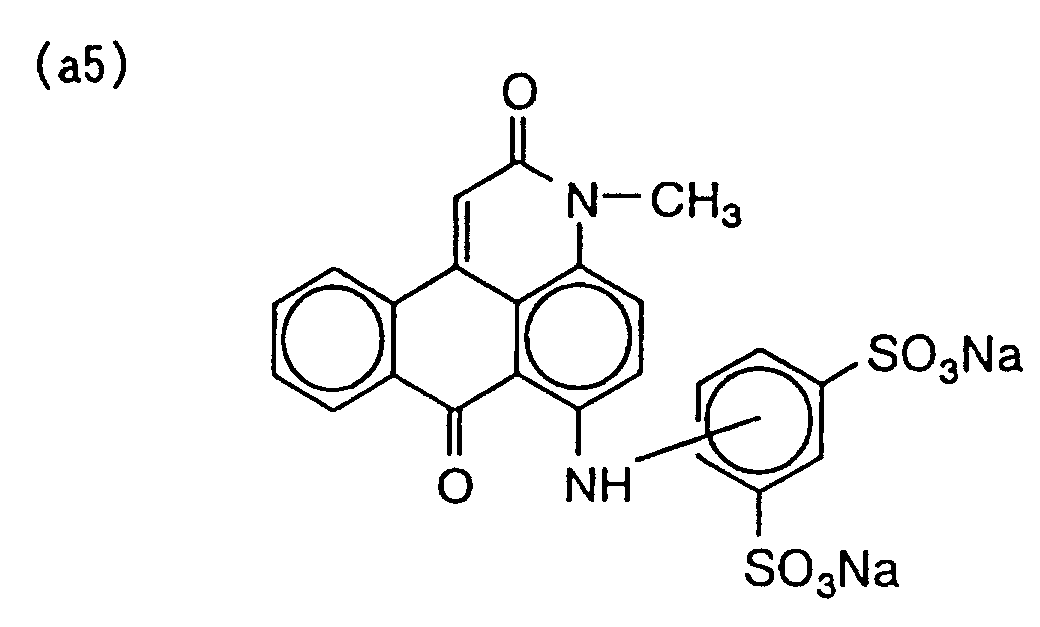
Examples 1 to 3 except that 0.15 g of dye (a5) was used in
place of dye (a6-1), thus a support having provided thereon
an antireflection layer and a filter layer was formed.
The spectral transmittance of each of the above-obtained
three kinds of supports was measured. Each of
them had an absorption maximum at 534 nm and 594 nm, and
the transmittance at absorption maximum at 534 nm was 65%
and that at 594 nm was 21%. The half value width of the
absorption maximum at 534 nm was 78 nm and that at 594 nm
was 28 nm.
(Production of front panel)
The polyethylene terephthalate film having provided
thereon an antireflection layer and a filter layer by means
of coating in the same manner as in Examples 1 to 3 was
stuck on the glass transparent support having provided
thereon an electromagnetic wave- and infrared ray-shielding
layer and an antireflection layer by means of coating in
the same manner as in Examples 1 to 3, thus a front panel
was prepared.
EXAMPLES 7 TO 9
(Formation of undercoat layer)
Undercoat layers were formed in the same manner as
in Examples 1 to 3.
(Formation of second undercoat layer)
Second undercoat layers were formed in the same
manner as in Examples 1 to 3.
(Formation of low refractive index layer)
A low refractive index layer was formed in the same
manner as in Examples 1 to 3.
(Formation of filter layer)
A filter layer was formed in the same manner as in
Examples 1 to 3 except that 0.05 g of dye (a1) was used in
place of dye (a6-1), thus a support having provided thereon
an antireflection layer and a filter layer was formed.
The spectral transmittance of each of the above-obtained
three kinds of supports was measured. Each of
them had an absorption maximum at 533 nm and 594 nm, and
the transmittance at absorption maximum at 533 nm was 63%
and that at 594 nm was 22%. The half value width of the
absorption maximum at 533 nm was 63 nm and that at 594 nm
was 29 nm.
(Production of front panel)
The polyethylene terephthalate film having provided
thereon an antireflection layer and a filter layer by means
of coating in the same manner as in Examples 1 to 3 was
stuck on the glass transparent support having provided
thereon an electromagnetic wave- and infrared ray-shielding
layer and an antireflection layer by means of coating in
the same manner as in Examples 1 to 3, thus the front panel
according to the present invention was prepared.
(Evaluation of filter function)
The front panel of the plasma display panel
(PDS4202J-H, manufactured by Fujitsu Limited) was removed
and each of the front panels prepared in Examples 1 to 9
was mounted on the body so that the filter layer faced the
image display surface of the plasma display panel. The
electromagnetic wave- and infrared ray-shielding layer was
connected to the ground metal plate on the back of the
plasma display panel, and the function was evaluated by
conducting the voltage induced on the electromagnetic wave-and
infrared ray-shielding layer by the electromagnetic
wave emitted from the plasma display panel to the ground
plate. The items which were evaluated were an
electromagnetic wave- and infrared ray-shielding
performance, the measurement of a contrast of the displayed
image and the evaluation of a color reproduction property
by visual observation.
The electromagnetic wave-shielding performance was
at least 9 dB or more in the range of the frequency of from
10 to 200 MHz with every sample in Examples 1 to 9, thus
the leakage level of electromagnetic waves restricted in
information processors and the like was achieved. Further,
the line spectrum-shielding performance in the near
infrared region was about 8% at 800 nm and 3% or less at
850 nm, thus the hindrance to the infrared ray remote-controlled
apparatus installed peripherally could be
prevented.
A contrast and a color reproduction property by
visual observation were conspicuously improved in all of
Examples 1 to 9. The contrast before replacing the front
panels was 10:1 but it was improved to 15:1 in all of the
examples. It was confirmed, as compared with the contrast
before replacing the front panels, that orangish red was
improved to pure red, greenish blue to clear blue and
yellowish white was improved to pure white.
EXAMPLE 10
(Formation of undercoat layer)
Both sides of a transparent polyethylene
terephthalate film (having a tensile impact strength of 784
kJ/m2) having a thickness of 100 µm were subjected to
corona discharge treatment, and then a latex (LX407C5,
manufactured by Zeon Corporation) made from a styrene-butadiene
copolymer having a refractive index of 1.55 and a
glass transition temperature of 37°C was coated on both
sides of the film, thereby undercoat layer was formed.
Coating was performed so as to obtain a dry thickness of
300 nm of the side of the film on which a filter layer was
to be provided, and 150 nm of the side on which a low
refractive index layer was to be provided.
(Formation of second undercoat layer)
Second undercoat layers were formed in the same
manner as in Examples 1 to 3.
(Formation of low refractive index layer)
A low refractive index layer was formed in the same
manner as in Examples 1 to 3.
(Formation of filter layer)
A filter layer was formed in the same manner as in
Examples 1 to 3 except that 0.05 g of dye (b13) and 0.15 g
of dye (a11) were used, thus selective absorption filter A
was formed.
The spectral transmittance of the above filter A
was measured. Filter A had absorption maximum at 535 nm
and 595 nm, and the transmittance at absorption maximum at
535 nm was 69% and that at 595 nm was 23%. The half value
width of the absorption maximum at 535 nm was 63 nm and
that at 595 nm was 30 nm. The surface reflectance was 1.2%.
EXAMPLE 11
Selective absorption filter B was prepared
according to the same procedure as in Example 10 except for
using a transparent triacetyl cellulose film (having a
tensile impact strength of 490 kJ/m2) having a thickness of
50 µm as the transparent support.
The spectral transmittance of the above filter B
was measured. Filter B had absorption maximum at 535 nm
and 595 nm, and the transmittance at absorption maximum at
535 nm was 71% and that at 595 nm was 22%. The half value
width of the absorption maximum at 535 nm was 64 nm and
that at 595 nm was 29 nm. The surface reflectance was 1.4%.
EXAMPLE 12
Selective absorption filter C was prepared
according to the same procedure as in Example 10 except for
using a transparent polycarbonate support (having a tensile
impact strength of 804 kJ/m2) having a thickness of 25 µm
as the transparent support.
The spectral transmittance of the above filter C
was measured. Filter C had absorption maximum at 535 nm
and 595 nm, and the transmittance at absorption maximum at
535 nm was 67% and that at 595 nm was 20%. The half value
width of the absorption maximum at 535 nm was 65 nm and
that at 595 nm was 28 nm. The surface reflectance was 1.3%.
COMPARATIVE EXAMPLE 1
Selective absorption filter D was prepared
according to the same procedure as in Example 10 except for
using a transparent polystyrene support (having a tensile
impact strength of 206 kJ/m2) having a thickness of 50 µm
as the transparent support.
The spectral transmittance of the above filter D
was measured. Filter D had absorption maximum at 535 nm
and 595 nm, and the transmittance at absorption maximum at
535 nm was 71% and that at 595 nm was 21%. The half value
width of the absorption maximum at 535 nm was 66 nm and
that at 595 nm was 31 nm. The surface reflectance was 1.3%.
COMPARATIVE EXAMPLE 2
Selective absorption filter E was prepared
according to the same procedure as in Example 10 except for
using a transparent triacetyl cellulose film (having a
tensile impact strength of 147 kJ/m2) having a thickness of
10 µm as the transparent support.
The spectral transmittance of the above filter E
was measured. Filter E had absorption maximum at 535 nm
and 595 nm, and the transmittance at absorption maximum at
535 nm was 71% and that at 595 nm was 25%. The half value
width of the absorption maximum at 535 nm was 62 nm and
that at 595 nm was 29 nm. The surface reflectance was 1.4%.
(Impact resistance test)
A front panel was produced by laminating Filters A
to E on a reinforced glass plate (10 cm square) having a
thickness of 3 mm with an adhesive. The height of 50%
breakage of this front panel was found according to JIS K
7211 "General rule of drop impact test of cured plastics".
A steel ball having a diameter of about 50 mm and a mass of
0.5 kg was used in the test. The criterion of breakage was
whether the reinforced glass plate was broken and separated
to small pieces or not. The results obtained are shown in
Table 1 below.
| Front Panel | Height of 50% Breakage (m) |
| Example 10 | 0.98 |
| Example 11 | 0.90 |
| Example 12 | 1.1 |
| Comparative Example 1 | 0.69 |
| Comparative Example 2 | 0.68 |
| Without a filter | 0.67 |
The front panel of the PDP display (PDS4202J-H:
manufactured by Fujitsu Limited) was removed and the back
film of the front panel was peeled off, and then Filters A
to E described in the above Examples and Comparative
Examples were stuck thereon with an adhesive. The contrast
of the display of each sample was measured and white and
red lights were evaluated. The results obtained are shown
in Table 2 below.
| Front Panel | Contrast | White Light | Red Light |
| Example 10 | 15:1 | White White (improved) | Red Red (improved) |
| Example 11 | 15:1 | White (improved) | Red (improved) |
| Example 12 | 15:1 | White (improved) | Red (improved) |
| Comparative Example 1 | 15:1 | White (improved) | Red (improved) |
| Comparative Example 2 | 15:1 | White (improved) | Red (improved) |
| Without a filter | 10:1 | Yellowish white | Orange |
As is apparent from the results in Examples and
Comparative Examples, by using the transparent film having
a tensile impact strength of 392 kJ/m2 or more as the
supports of a filter layer and an antireflection layer, a
front panel can be provided with impact resistance.
EXAMPLE 13
(Formation of undercoat layer)
Both sides of a transparent biaxially stretched
polyethylene terephthalate film having a thickness of 175
µm were subjected to corona discharge treatment, and then a
latex (LX407C5, manufactured by Zeon Corporation) made from
a styrene-butadiene copolymer having a refractive index of
1.55 and a glass transition temperature of 37°C was coated
on both sides of the film, thereby undercoat layers were
formed. Coating was performed so as to obtain a dry
thickness of 300 nm of one side and 150 nm of the other
side.
(Formation of filter layer)
A 1N sodium hydroxide solution was added to 180 g
of a 10 wt% gelatin aqueous solution so that pH became 7,
dye (b13) was added thereto in an arbitrary amount, and the
mixed solution was stirred at 30°C for 24 hours. The thus-obtained
coating solution for a filter layer was coated on
the side of the transparent support on which the undercoat
layer having a thickness of 300 nm was coated in a coating
amount of dye (b13) of 15 mg/m2, and the coated layer was
dried at 120°C for 10 minutes, thereby a filter layer was
obtained. The weight ratio of dye/gelatin of each filter
layer of Samples A-1 to A-6 prepared above are shown in
Table 1 below.
(Formation of low refractive index layer as antireflection
layer)
To 2.50 g of a reactive fluorine-containing polymer
(JN-7225, manufactured by JSR Corporation) was added 5.0 g
of MIBK and stirred at room temperature for 10 minutes, and
the mixed solution was filtered through a polypropylene
filter of 1 µm. The thus-obtained coating solution was
coated on the side opposite to the side on which the filter
layer was provided of Samples 1 to 6 in a dry coating
thickness of 96 nm by means of a bar coater and dried at
120°C for 15 minutes to cure the coated layer, thereby a
low refractive index layer was formed.
EXAMPLE 14
Samples B-1 to B-6 were prepared in the same manner
as the preparation of Samples A-1 to A-6 except that dye
(b13) was replaced with dye (b16).
(Evaluation of filter function)
The outermost surface film of the front panel of
the plasma display panel (PDS4202J-H, manufactured by
Fujitsu Limited) (E face of the plasma display shown in Fig.
1 above) was peeled off, and the optical filters produced
in Example 13 or 14 (the surface of the side on which a low
refractive index layer was not provided) were stuck thereon
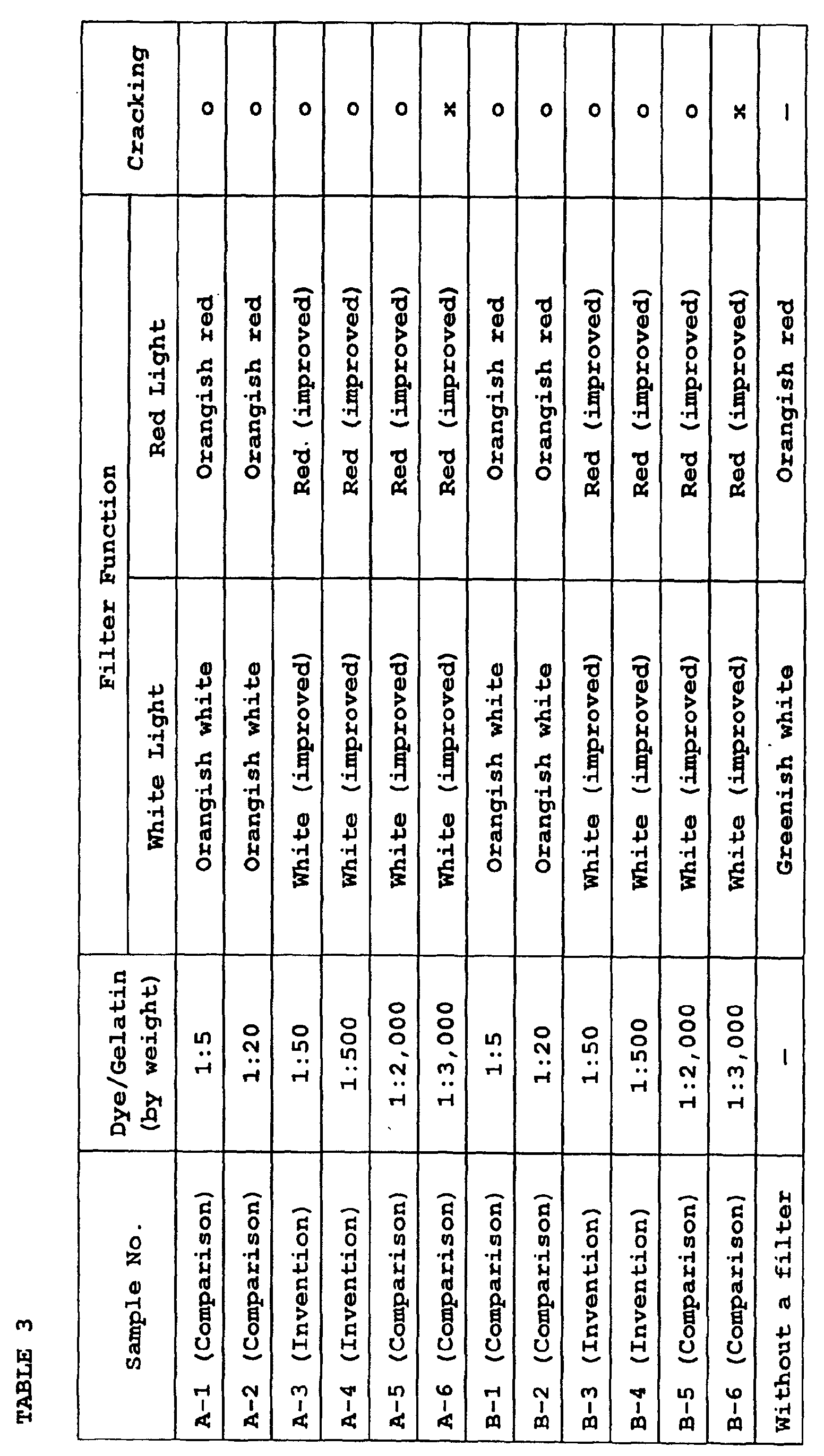
with an adhesive. Cracking of the optical filters and
white light and red light of the displayed images were
visually evaluated. The results obtained are shown in
Table 3 below.
As is apparent from the above results, filters
having no cracking and capable of correcting color balance
of PDP can be obtained by the ratio of dye/binder of the
filter layer falling within the range of from 1:50 to
1:2,000. Further, the same results can be obtained when
the face of sample sticking is not only E face but F face
and G face in Fig. 1.
Industrial Application
The front panel according to the present invention
can be applied to image displays such as a liquid crystal
display (LCD), a plasma display panel (PDP), an electroluminescence
display (ELD), and a cathode ray tube (CRT),
in particular, when used as the front panels of a plasma
display panel (PDP) and a cathode ray tube (CRT),
conspicuous effect can be obtained.