EP1186901A2 - Verfahren und Vorrichtung zur Erzeugung digitaler Signalmuster - Google Patents
Verfahren und Vorrichtung zur Erzeugung digitaler Signalmuster Download PDFInfo
- Publication number
- EP1186901A2 EP1186901A2 EP01115838A EP01115838A EP1186901A2 EP 1186901 A2 EP1186901 A2 EP 1186901A2 EP 01115838 A EP01115838 A EP 01115838A EP 01115838 A EP01115838 A EP 01115838A EP 1186901 A2 EP1186901 A2 EP 1186901A2
- Authority
- EP
- European Patent Office
- Prior art keywords
- signal pattern
- signal
- group
- patterns
- address
- Prior art date
- Legal status (The legal status is an assumption and is not a legal conclusion. Google has not performed a legal analysis and makes no representation as to the accuracy of the status listed.)
- Granted
Links
Images
Classifications
-
- G—PHYSICS
- G11—INFORMATION STORAGE
- G11C—STATIC STORES
- G11C29/00—Checking stores for correct operation ; Subsequent repair; Testing stores during standby or offline operation
- G11C29/04—Detection or location of defective memory elements, e.g. cell constructio details, timing of test signals
- G11C29/08—Functional testing, e.g. testing during refresh, power-on self testing [POST] or distributed testing
- G11C29/10—Test algorithms, e.g. memory scan [MScan] algorithms; Test patterns, e.g. checkerboard patterns
-
- G—PHYSICS
- G01—MEASURING; TESTING
- G01R—MEASURING ELECTRIC VARIABLES; MEASURING MAGNETIC VARIABLES
- G01R31/00—Arrangements for testing electric properties; Arrangements for locating electric faults; Arrangements for electrical testing characterised by what is being tested not provided for elsewhere
- G01R31/28—Testing of electronic circuits, e.g. by signal tracer
- G01R31/317—Testing of digital circuits
- G01R31/3181—Functional testing
- G01R31/3183—Generation of test inputs, e.g. test vectors, patterns or sequences
Definitions
- the invention relates to a method and a device to generate electrical digital signal patterns according to Preambles of the independent claims 1 and 10.
- Such a method and such an apparatus are known from US 6 014 764.
- the signal patterns should already be in the final form must be provided be cached. This may be a very large memory required.
- pattern data are stored in a local memory and are by addressing the memory using an address control read out and output.
- a so-called “Pattern chaining definition” for a set of patterns designated pattern indicates the order in which this Patterns can be read from the memory.
- This pattern Chaining definition can be structured as a so-called pattern list and stored in the same memory. With help This pattern list allows you to chain the patterns together or individual patterns repeated in loop repetitions output. However, the patterns are not in the pattern list stored itself, but the 30 bit pointer addresses, which indicate in memory where the pattern area begins and ends.
- the above object is achieved according to a first aspect by a method for generating digital electrical signal patterns, in which one in an addressable memory Multitude of different signal patterns or signal pattern groups, each with a variety of different signal patterns included, formed and this signal pattern or the Signal pattern groups each on the respective signal pattern or the group's own address in memory stored in advance and on an appropriate addressing read out and made available, whereby in the memory also a reading order of the stored Determine signal patterns or signal pattern groups Definition is saved, characterized in that the definition determining the reading order by a in memory at the same address as each stored Signal patterns or each signal pattern group previously stored Jump address is specified, which is a storage location for a next signal pattern to be read or a next one assigns signal pattern group to be read, and that depends from the current address and from a supplied one Control signal either the current signal pattern or signal pattern groups in the by the consecutive address or their storage order or in an order order determined by the respective jump address (P) be read from the memory.
- a method for generating digital electrical signal patterns in which one in an
- the control signal can be a simple digital yes-no signal his.
- each signal pattern group specified by an address the same number of signal patterns, for example four signal patterns.
- each signal pattern group also a different number of signal patterns to have.
- One set up to carry out the method according to the invention Device is characterized by a Buffer register with minimal register size, which used to store the signal pattern groups mentioned connected control logic circuit for addressing of the buffer register and for receiving said Control signal.
- a Buffer register with minimal register size which used to store the signal pattern groups mentioned connected control logic circuit for addressing of the buffer register and for receiving said Control signal.
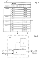
- Fig. 1 shows in tabular form the memory organization of one Designed implementation of the inventive method Buffer register 1 used for generation 3-bit bank select signals for testing 256M SDRAMs, who have four memory banks.
- Buffer register 1 used for generation 3-bit bank select signals for testing 256M SDRAMs, who have four memory banks.
- the buffer register 1 are among the sixteen 4-bit addresses specified in column A. 0000-1111 in column B sixteen three bit positions Signal pattern groups with BS [1], BS [0], A [10] each with a sequence of four patterns HSC1, HSC2, HSC3 and HSC4 saved.
- In the last column C there is a jump address P for a subsequent signal pattern group to an address in Column A indicated at which when the control signal S is activated is jumping.
- control signal S If the control signal S is activated, after the full output of those selected by the current address Signal pattern group jump to the beginning of the the jump address P stored in column C. following group. This can then depend on the control signal also read out or exited cyclically repeatedly become.
- Fig. 2 is an embodiment of a BOST solution designed device according to the invention and shows schematically as a block diagram in a BOST block (BOST: Build Outside Self Test) implemented buffer register 1 in conjunction with a control logic circuit 2.
- BOST Build Outside Self Test
- the address BSA for the current selection of a particular one Signal pattern group in the buffer register 1 can in BOST block generated or from outside by a test system be fed.
- the control signal is also from the test system S fed.
- the with the device according to the invention generated signal pattern HSC 1, 2, 3, 4 become one digital semiconductor circuit to be tested DUT, for example an SDRAM.
- the method according to the invention can also be used periodically Generation of signal patterns for other applications use.
- the inventive method for generation of signal patterns for cyclically varying data signals, Control signals etc. when testing high-speed semiconductor memory devices pointed.
- the method according to the invention relates and the device according to the invention a system for generation of digital electrical signal patterns from one predetermined amount of available individual signals, whereby neither complex algorithmic systems nor complex Memory are necessary. Instead, the Invention such a signal pattern generation with a minimal Register size and simple control logic.
Landscapes
- Engineering & Computer Science (AREA)
- General Engineering & Computer Science (AREA)
- Physics & Mathematics (AREA)
- General Physics & Mathematics (AREA)
- Tests Of Electronic Circuits (AREA)
- For Increasing The Reliability Of Semiconductor Memories (AREA)
Abstract
Description
- Fig. 1
- zeigt schematisch eine beispielhafte Speicherorganisation eines zur Speicherung von Signalmustergruppen verwendeten kleinen Zwischenspeicherregisters,
- Fig. 2
- zeigt in Form eines Blockschaltbilds, das in Fig. 1 gezeigte Zwischenspeicherregister in Verbindung mit einer Steuerlogikschaltung.
Claims (11)
- Verfahren zur Erzeugung digitaler elektrischer Signalmuster, bei dem in einem adressierbaren Speicher (1) eine Vielzahl unterschiedlicher Signalmuster oder Signalmustergruppen, die jeweils eine Vielzahl unterschiedlicher Signalmuster (HSC1, HSC2, HSC3, HSC4) enthalten, gebildet und diese Signalmuster oder die Signalmustergruppen jeweils an einer dem jeweiligen Signalmuster oder der jeweiligen Gruppe eigenen Adresse im Speicher vorab gespeichert und auf eine entsprechende Adressierung hin ausgelesen und zur Verfügung gestellt werden, wobei im Speicher außerdem eine eine Auslesereihenfolge der gespeicherten Signalmuster oder Signalmustergruppen bestimmende Definition gespeichert wird,
dadurch gekennzeichnet, dass die die Auslesereihenfolge bestimmende Definition durch eine im Speicher (1) unter derselben Adresse (BSA) wie jedes gespeicherte Signalmuster oder jede Signalmustergruppe vorab gespeicherte Sprungadresse (P) angegeben ist, die eine Speicherposition für ein nächstes auszulesendes Signalmuster oder eine nächste auszulesende Signalmustergruppe zuordnet, und
dass abhängig von der jeweils aktuellen Adresse (BSA) und von einem zugeführten Steuersignal (S) entweder die aktuellen Signalmuster oder Signalmustergruppen in der durch die fortlaufende Adresse bzw. ihre Speicherfolge angegebenen Reihenfolge oder in einer durch die jeweilige Sprungadresse (P) bestimmten Reihenfolge aus dem Speicher (1) ausgelesen werden. - Verfahren nach Anspruch 1,
dadurch gekennzeichnet, dass jede durch eine Adresse angegebene Signalmustergruppe die gleiche Anzahl von Signalmustern enthält. - Verfahren nach Anspruch 1 oder 2,
dadurch gekennzeichnet, dass jede durch eine Adresse angegebene Signalmustergruppe vier Signalmuster aufweist. - Verfahren nach Anspruch 1,
dadurch gekennzeichnet, dass einige oder alle Signalmustergruppen eine unterschiedliche Anzahl von Signalmustern enthalten. - Verfahren nach einem der vorangehenden Ansprüche,
dadurch gekennzeichnet, dass jedes Signalmuster drei Bitstellen hat. - Verfahren nach einem der vorangehenden Ansprüche,
dadurch gekennzeichnet, dass, wenn das Steuersignal (S) nicht aktiviert ist, fortlaufend das aktuell adressierte Signalmuster bzw. die Signalmuster der aktuell adressierten Signalmustergruppe ausgegeben wird bzw. werden. - Verfahren nach einem der Ansprüche 1 bis 5,
dadurch gekennzeichnet, dass, wenn das Steuersignal (S) nicht aktiviert ist, fortlaufend die gespeicherten Signalmuster oder die Signalmustergruppen in der durch die fortlaufende Adressierung bzw. ihre Speicherfolge angegebenen Reihenfolge ausgegeben werden und dass nach Ausgabe des letzten Signalmusters mit der Ausgabe des ersten gespeicherten Signalmusters bzw. des ersten Signalmusters der ersten Gruppe fortgefahren wird. - Verfahren nach einem der Ansprüche 1 bis 5,
dadurch gekennzeichnet, dass, wenn das Steuersignal (S) aktiviert ist, nach der vollständigen Ausgabe des aktuell adressierten Signalmusters bzw. der adressierten Signalmustergruppe der Sprung zu dem durch die Sprungadresse (P) zugeordneten nächsten Signalmuster oder zum Anfang der durch die Sprungadresse (P) zugeordneten nächsten Signalmustergruppe erfolgt. - Verwendung des Verfahrens nach einem der Ansprüche 1 bis 8 zur Ausgabe einer Folge von Dreibit-Signalmustern für die Bank-Select-Signale beim Test schneller dynamischer Halbleiterspeicherbausteine, insbesondere 256 M SDRAMs mit vier Speicherbänken.
- Vorrichtung zur Durchführung des Verfahrens nach einem der Ansprüche 1 bis 8,
gekennzeichnet durch
eine mit einem Zwischenspeicherregister (1), das als der adressierbare Speicher zur Speicherung der Signalmuster bzw. Signalmustergruppen und der Sprungadresse (P) eingerichtet ist, verbundene Steuerlogikschaltung (2) zur Erzeugung von Adressen für das Zwischenspeicherregister (1). - Vorrichtung nach Anspruch 10,
dadurch gekennzeichnet, dass sie in einer von einem herkömmlichen Testgerät abgesetzten integrierten Halbleiterschaltung (BOST) für den Test von schnellen dynamischen Digitalschaltungen, insbesondere SDRAM-Speicherbausteinen zur Erzeugung von Bank-Select-Signalen vorgesehen ist.
Applications Claiming Priority (2)
| Application Number | Priority Date | Filing Date | Title |
|---|---|---|---|
| DE10034854 | 2000-07-18 | ||
| DE10034854A DE10034854A1 (de) | 2000-07-18 | 2000-07-18 | Verfahren und Vorrichtung zur Erzeugung digitaler Signalmuster |
Publications (3)
| Publication Number | Publication Date |
|---|---|
| EP1186901A2 true EP1186901A2 (de) | 2002-03-13 |
| EP1186901A3 EP1186901A3 (de) | 2005-06-22 |
| EP1186901B1 EP1186901B1 (de) | 2007-02-14 |
Family
ID=7649290
Family Applications (1)
| Application Number | Title | Priority Date | Filing Date |
|---|---|---|---|
| EP01115838A Expired - Lifetime EP1186901B1 (de) | 2000-07-18 | 2001-06-28 | Verfahren und Vorrichtung zur Erzeugung digitaler Signalmuster |
Country Status (4)
| Country | Link |
|---|---|
| US (1) | US7117403B2 (de) |
| EP (1) | EP1186901B1 (de) |
| DE (2) | DE10034854A1 (de) |
| TW (1) | TW550392B (de) |
Families Citing this family (3)
| Publication number | Priority date | Publication date | Assignee | Title |
|---|---|---|---|---|
| US7437638B2 (en) * | 2002-11-12 | 2008-10-14 | Agilent Technologies, Inc. | Boundary-Scan methods and apparatus |
| US20070226553A1 (en) * | 2006-03-21 | 2007-09-27 | Khaled Fekih-Romdhane | Multiple banks read and data compression for back end test |
| CN110008075A (zh) * | 2018-01-05 | 2019-07-12 | 深圳市中兴微电子技术有限公司 | 一种芯片调试方法及装置 |
Family Cites Families (7)
| Publication number | Priority date | Publication date | Assignee | Title |
|---|---|---|---|---|
| JPS5990067A (ja) * | 1982-11-15 | 1984-05-24 | Advantest Corp | 論理回路試験用パタ−ン発生装置 |
| US6014764A (en) * | 1997-05-20 | 2000-01-11 | Schlumberger Technologies Inc. | Providing test vectors with pattern chaining definition |
| US6073263A (en) * | 1997-10-29 | 2000-06-06 | Credence Systems Corporation | Parallel processing pattern generation system for an integrated circuit tester |
| US6070227A (en) * | 1997-10-31 | 2000-05-30 | Hewlett-Packard Company | Main memory bank indexing scheme that optimizes consecutive page hits by linking main memory bank address organization to cache memory address organization |
| US6108745A (en) * | 1997-10-31 | 2000-08-22 | Hewlett-Packard Company | Fast and compact address bit routing scheme that supports various DRAM bank sizes and multiple interleaving schemes |
| US6009546A (en) * | 1998-07-30 | 1999-12-28 | Credence Systems Corporation | Algorithmic pattern generator |
| US6154715A (en) * | 1999-01-15 | 2000-11-28 | Credence Systems Corporation | Integrated circuit tester with real time branching |
-
2000
- 2000-07-18 DE DE10034854A patent/DE10034854A1/de not_active Withdrawn
-
2001
- 2001-06-28 DE DE50112029T patent/DE50112029D1/de not_active Expired - Lifetime
- 2001-06-28 EP EP01115838A patent/EP1186901B1/de not_active Expired - Lifetime
- 2001-07-17 TW TW090117425A patent/TW550392B/zh not_active IP Right Cessation
- 2001-07-18 US US09/907,777 patent/US7117403B2/en not_active Expired - Fee Related
Also Published As
| Publication number | Publication date |
|---|---|
| DE10034854A1 (de) | 2002-02-14 |
| US7117403B2 (en) | 2006-10-03 |
| TW550392B (en) | 2003-09-01 |
| EP1186901A3 (de) | 2005-06-22 |
| EP1186901B1 (de) | 2007-02-14 |
| DE50112029D1 (de) | 2007-03-29 |
| US20020009007A1 (en) | 2002-01-24 |
Similar Documents
| Publication | Publication Date | Title |
|---|---|---|
| DE60012966T2 (de) | Hochgeschwindigkeitsfehlererfassungsgerät und verfahren für automatische testeinrichtung | |
| DE10010440B4 (de) | Synchrones dynamisches Speicherbauelement mit wahlfreiem Zugriff und Verfahren zur CAS-Latenzsteuerung | |
| DE69232458T2 (de) | Programmierbare Zeitsteuerung für Speicher | |
| DE69729771T2 (de) | Integrierte Schaltung mit einer eingebauten Selbsttestanordnung | |
| DE69229104T2 (de) | Stroboskopische Signale in Halbleiterspeicheranordnungen | |
| DE69326493T2 (de) | Zugriffsverfahren für eine synchrone Halbleiterspeicheranordnung | |
| DE19823931C2 (de) | Testmustergeneratorschaltung für ein IC-Testgerät | |
| DE69720158T2 (de) | Speicherschaltungen mit eingebautem Selbsttest | |
| DE4206286C2 (de) | Speicherzugriffssystem und Verfahren zum Ausgeben eines digitalen Datenstromes | |
| DE102005051308A1 (de) | Zentrale Vorrichtung zum Testen von Speicher und Verfahren | |
| DE3237224A1 (de) | Vorrichtung zum erzeugen einer folge von pruefdaten fuer lsi-schaltungen | |
| DE69120301T2 (de) | Speicherprüfgerät | |
| DE3689414T2 (de) | Automatisches Prüfsystem mit "wahrem Prüfer-per-Anschluss" -Architektur. | |
| DE60114233T2 (de) | Gewichteter zufallsmustertest mit vorgespeicherten gewichten | |
| DE4034167C2 (de) | ||
| DE10296525B4 (de) | Chipinterne Schaltungen für ein Hochgeschwindigkeitsspeichertesten mit einem langsamen Speichertester | |
| DE19950347B4 (de) | Mustergenerator für Halbleiterprüfsysteme | |
| DE10297436T5 (de) | Zeitgenerator und Prüfvorrichtung | |
| DE19951205A1 (de) | Testmustergenerator; Speichertestvorrichtung und Verfahren zur Erzeugung einer Mehrzahl von Testmustern | |
| DE10115879C1 (de) | Testdatengenerator | |
| DE10135966B4 (de) | Verfahren und Vorrichtung zum On-Chip-Testen von Speicherzellen einer integrierten Speicherschaltung | |
| DE102007013761B4 (de) | Speicher mit einem Schreibtrainingsblock | |
| DE102006030373A1 (de) | Halbleiterspeichervorrichtung | |
| EP1186901A2 (de) | Verfahren und Vorrichtung zur Erzeugung digitaler Signalmuster | |
| DE19781563C2 (de) | Mustergenerator |
Legal Events
| Date | Code | Title | Description |
|---|---|---|---|
| PUAI | Public reference made under article 153(3) epc to a published international application that has entered the european phase |
Free format text: ORIGINAL CODE: 0009012 |
|
| AK | Designated contracting states |
Kind code of ref document: A2 Designated state(s): AT BE CH CY DE DK ES FI FR GB GR IE IT LI LU MC NL PT SE TR |
|
| AX | Request for extension of the european patent |
Free format text: AL;LT;LV;MK;RO;SI |
|
| PUAL | Search report despatched |
Free format text: ORIGINAL CODE: 0009013 |
|
| AK | Designated contracting states |
Kind code of ref document: A3 Designated state(s): AT BE CH CY DE DK ES FI FR GB GR IE IT LI LU MC NL PT SE TR |
|
| AX | Request for extension of the european patent |
Extension state: AL LT LV MK RO SI |
|
| RIC1 | Information provided on ipc code assigned before grant |
Ipc: 7G 11C 29/00 A |
|
| 17P | Request for examination filed |
Effective date: 20051128 |
|
| AKX | Designation fees paid |
Designated state(s): DE GB IE |
|
| GRAP | Despatch of communication of intention to grant a patent |
Free format text: ORIGINAL CODE: EPIDOSNIGR1 |
|
| GRAS | Grant fee paid |
Free format text: ORIGINAL CODE: EPIDOSNIGR3 |
|
| GRAA | (expected) grant |
Free format text: ORIGINAL CODE: 0009210 |
|
| AK | Designated contracting states |
Kind code of ref document: B1 Designated state(s): DE GB IE |
|
| PG25 | Lapsed in a contracting state [announced via postgrant information from national office to epo] |
Ref country code: IE Free format text: LAPSE BECAUSE OF FAILURE TO SUBMIT A TRANSLATION OF THE DESCRIPTION OR TO PAY THE FEE WITHIN THE PRESCRIBED TIME-LIMIT Effective date: 20070214 |
|
| REG | Reference to a national code |
Ref country code: GB Ref legal event code: FG4D Free format text: NOT ENGLISH |
|
| REF | Corresponds to: |
Ref document number: 50112029 Country of ref document: DE Date of ref document: 20070329 Kind code of ref document: P |
|
| REG | Reference to a national code |
Ref country code: IE Ref legal event code: FG4D Free format text: LANGUAGE OF EP DOCUMENT: GERMAN |
|
| GBV | Gb: ep patent (uk) treated as always having been void in accordance with gb section 77(7)/1977 [no translation filed] |
Effective date: 20070214 |
|
| REG | Reference to a national code |
Ref country code: IE Ref legal event code: FD4D |
|
| PG25 | Lapsed in a contracting state [announced via postgrant information from national office to epo] |
Ref country code: GB Free format text: LAPSE BECAUSE OF FAILURE TO SUBMIT A TRANSLATION OF THE DESCRIPTION OR TO PAY THE FEE WITHIN THE PRESCRIBED TIME-LIMIT Effective date: 20070214 |
|
| PLBE | No opposition filed within time limit |
Free format text: ORIGINAL CODE: 0009261 |
|
| STAA | Information on the status of an ep patent application or granted ep patent |
Free format text: STATUS: NO OPPOSITION FILED WITHIN TIME LIMIT |
|
| 26N | No opposition filed |
Effective date: 20071115 |
|
| PGFP | Annual fee paid to national office [announced via postgrant information from national office to epo] |
Ref country code: DE Payment date: 20140723 Year of fee payment: 14 |
|
| REG | Reference to a national code |
Ref country code: DE Ref legal event code: R081 Ref document number: 50112029 Country of ref document: DE Owner name: INFINEON TECHNOLOGIES AG, DE Free format text: FORMER OWNER: QIMONDA AG, 81739 MUENCHEN, DE Ref country code: DE Ref legal event code: R081 Ref document number: 50112029 Country of ref document: DE Owner name: POLARIS INNOVATIONS LTD., IE Free format text: FORMER OWNER: QIMONDA AG, 81739 MUENCHEN, DE |
|
| REG | Reference to a national code |
Ref country code: DE Ref legal event code: R081 Ref document number: 50112029 Country of ref document: DE Owner name: POLARIS INNOVATIONS LTD., IE Free format text: FORMER OWNER: INFINEON TECHNOLOGIES AG, 85579 NEUBIBERG, DE |
|
| REG | Reference to a national code |
Ref country code: DE Ref legal event code: R119 Ref document number: 50112029 Country of ref document: DE |
|
| PG25 | Lapsed in a contracting state [announced via postgrant information from national office to epo] |
Ref country code: DE Free format text: LAPSE BECAUSE OF NON-PAYMENT OF DUE FEES Effective date: 20160101 |