EP1186097B1 - Verstärkerschaltung - Google Patents
Verstärkerschaltung Download PDFInfo
- Publication number
- EP1186097B1 EP1186097B1 EP00931389A EP00931389A EP1186097B1 EP 1186097 B1 EP1186097 B1 EP 1186097B1 EP 00931389 A EP00931389 A EP 00931389A EP 00931389 A EP00931389 A EP 00931389A EP 1186097 B1 EP1186097 B1 EP 1186097B1
- Authority
- EP
- European Patent Office
- Prior art keywords
- signal
- reflection
- signal path
- circuit
- reflection amplifiers
- Prior art date
- Legal status (The legal status is an assumption and is not a legal conclusion. Google has not performed a legal analysis and makes no representation as to the accuracy of the status listed.)
- Expired - Lifetime
Links
Images

Classifications
-
- H—ELECTRICITY
- H03—ELECTRONIC CIRCUITRY
- H03F—AMPLIFIERS
- H03F3/00—Amplifiers with only discharge tubes or only semiconductor devices as amplifying elements
- H03F3/60—Amplifiers in which coupling networks have distributed constants, e.g. with waveguide resonators
- H03F3/608—Reflection amplifiers, i.e. amplifiers using a one-port amplifying element and a multiport coupler
-
- H—ELECTRICITY
- H03—ELECTRONIC CIRCUITRY
- H03F—AMPLIFIERS
- H03F2201/00—Indexing scheme relating to details of amplifiers with only discharge tubes, only semiconductor devices or only unspecified devices as amplifying elements covered by H03F1/00
- H03F2201/32—Indexing scheme relating to modifications of amplifiers to reduce non-linear distortion
- H03F2201/3215—To increase the output power or efficiency
Definitions
- This invention relates to an amplifier circuit, in particular but not exclusively to an amplifier circuit for providing bandpass amplification at intermediate frequencies in radio receivers.
- Amplifiers are widely used in the prior art for amplifying input signals applied thereto to provide amplified output signals. This is particularly important in radio receivers in which radiation received thereat generates corresponding antenna received signals which typically have an amplitude of microvolts.
- the radio receivers employ amplifiers therein to amplify such received signals to an amplitude in the order of millivolts to volts, for example to drive a loudspeaker. Since it is difficult to prevent amplifiers designed to amplify at radio frequencies from spontaneously oscillating, especially if they comprise cascaded gain providing stages, it is customary to heterodyne the received signals to lower intermediate frequencies whereat it is easier to provide a high degree of amplification and also provide more selective bandpass signal filtration.
- a radio receiver receives radiation at a frequency of 500 MHz and generates a corresponding antenna received signal also at 500 MHz.
- the receiver heterodynes the received signal to generate an intermediate frequency signal in a frequency range around 10.7 MHz which is then amplified and filtered, and finally demodulates the amplified intermediate frequency signal to generate a corresponding audio output signal having signal components in a frequency range of 100 Hz to 5 kHz.
- UHF ultra high frequency
- intermediate frequency amplifier circuits In modern mobile telephones, most signal amplification is provided in intermediate frequency amplifier circuits incorporated therein. These circuits comprise transmission amplifiers and associated surface acoustic wave (SAW) or ceramic filters to provide a narrow bandpass signal amplification characteristic; the circuits and their associated filters are conventionally referred to collectively as an "intermediate frequency strip". Such transmission amplifiers consume significant power in operation, for example intermediate frequency amplifier circuits employed in mobile telephones typically consume between several hundred microamperes and several mA of current when operational.
- SAW surface acoustic wave
- the inventor has appreciated, rather than concentrating on improving battery technology, that reduction in current consumption of intermediate frequency amplifier circuits in radio receivers is desirable to provide extended operating time from batteries.
- the invention has therefore been made in a endeavour to provide an alternative type of amplifier circuit, for example a circuit especially suitable for use at intermediate frequencies in radio receivers which is capable of requiring less power to operate.
- an amplifier circuit for receiving an input signal and providing a corresponding amplified output signal, the circuit characterised in that it comprises:
- the invention provides the advantage that incorporation of the delaying means enables the switching means to partition the input signal into discrete segments which are stored for a period of time within the delaying means, thereby providing the switching means with time to direct the segments in the forward direction along the signal path and prevent them from flowing in the reverse direction along the path which would give rise to spontaneous oscillation.
- the circuit addresses this problem by incorporating the connecting means which promotes intended signal amplification in the circuit and counteracts signal amplification giving rise to spontaneous oscillation therein.
- Spontaneous oscillation is defined as self induced oscillation arising along a signal path providing amplification as a consequence of feedback occurring around or within the signal path.
- the delaying means comprises a plurality of delay lines, such that a delay line is interposed between each reflection amplifier and the switching means.
- the delay lines are operative to provide bandpass signal transmission therethrough.
- the amplifier circuit is capable of providing a bandpass transmission characteristic appropriate for intermediate frequency amplifiers for use in, for example, radio receivers and mobile telephones.
- the invention provides a method of amplifying an input signal and providing a corresponding amplified output signal, the method including the steps of:
- the method provides the advantage that, during amplification, the signal is selectively directed from amplifier to amplifier in a forward direction along the signal path, thereby counteracting any of the amplifiers reamplifying the input signal and hence preventing any feedback loops being established in which spontaneous oscillation can arise.
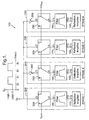
- the circuit 100 comprises four reflection amplifiers 110, 120, 130, 140, four bandpass filter delay elements 150, 160, 170, 180, four switches 200, 210, 220, 230 and two logic inverters 250, 260.
- the amplifiers 110, 120, 130, 140 in combination with their associated delay elements 150, 160, 170, 180 and their switches 200, 210, 220, 230 are connected to form STAGE 1, STAGE 2, STAGE 3, STAGE 4 respectively.
- the STAGES 1-4 are shown within dotted lines 300-330 respectively.
- the STAGE 2 and STAGE 4 also incorporate the inverters 250, 260 respectively.
- Each filter element 150, 160, 170, 180 incorporates a first signal port T1 and a second signal port T2.
- the filter elements 150, 160, 170, 180 each provide bandpass signal filtration as well as providing signal storage, for a period ⁇ , thereby providing signal propagation delay therethrough.
- the filter elements are mutually identical, namely providing an identical bandpass transmission characteristic with mutually similar centre frequencies, and can each be implemented as individual devices or fabricated integrally onto a single substrate.
- the reflection amplifiers 110, 120, 130, 140 are mutually identical and employ a circuit configuration as shown in Figure 2. Such reflection amplifiers are also described in our UK Patent number GB 2 284 323B which is herein incorporated by reference.
- Each amplifier 110, 120, 130, 140 incorporates an input/output port T3 whereat signals are received and then reflected with increased magnitude on account of a negative resistance being presented at the port T3 during operation.
- the switches 200, 210, 220, 230 are also mutually identical. Each switch incorporates a wiper terminal A, two switch pole terminals B and C, and a switch control terminal D for receiving a binary switching signal which altemates in operation between a logic state 0 and a logic state 1. When the binary signal is in the logic state 0, the terminal A is connected to the terminal B. Conversely, the terminal A is connected to the terminal C when the binary signal is in the logic state 1.
- the terminals D of the switches 210, 230 are connected through the inverters 250, 260 respectively to an applied control line represented by S c . Moreover, the terminals D of switches 200, 220 are connected directly to the control line S c . Thus, in operation, the switches 200, 220 are oppositely connected relative to the switches 210, 230 by virtue of relative wiper positions.
- the terminal A is connected to the port T1, and the port T2 is connected to the port T3.
- the terminal B of the STAGE 1 is connected to receive an input signal S in
- the terminal C of STAGE 4 is connected to output an output signal S out .
- the terminals C of the STAGES 1-3 are connected to the terminals B of the STAGES 2-4 respectively.
- the control signal S c is in the logic state 0 so that the terminals A of switches 200, 220 are connected to the terminals B thereof, and the terminals A of switches 210, 230 are connected to the terminals C thereof.
- the signal S in passes to the terminal B of the switch 200 and continues therethrough from the terminal A to the port T1 of the filter element 150.
- the signal S c switches to the logic state 1 which connects the terminals A of the switches 200, 220 to the terminals C thereof, and connects the terminals A of the switches 210, 230 to the terminals B thereof.
- the signal S c switches back to the logic state 0 which reconnects the terminals A of the switches 200, 220 to the terminals C thereof, and connects the terminals A of the switches 210, 230 to the terminals B thereof.
- This mutually isolates STAGES 1 and 2, and likewise STAGES 3 and 4, thereby preventing signals passing back towards the terminal B of the STAGE 1, thereby counteracting spontaneous oscillation arising due to reflection of radiation between a stage and its preceding stage.
- Incorporating the switches 200, 210, 220, 230 to periodically isolate the amplifiers 110, 120, 130, 140 as described above provides the advantage of interrupting the formation of standing waves within the circuit 100, thereby counteracting spontaneous oscillation therein. This allows higher signal amplification approaching + 30 dB for each stage, for example, to be achieved. If the switches were omitted and the terminals T1 of the filter elements connected together to form a common input/output node, severe oscillation problems would arise in the circuit 100 due to uninterrupted signal reflection from stage to stage.
- the circuit 100 thus provides pseudo - continuous amplification which is interrupted periodically at intervals of 4 ⁇ for a period 2 ⁇ . Moreover, signals require a period of 8 ⁇ to propagate through the circuit 100.
- the output signal S out is subsequently demodulated and high frequency artefacts arising thereby from the pseudo-continuous nature of the signal S out are removed by filtration.
- the circuit 100 can be modified in a number of ways to provide modified circuits, namely;
- a circuit for each of the amplifiers 110-140 is indicated by 400.
- the circuit 400 is included within a dotted line 410 and comprises a silicon or gallium arsenide (GaAs) transistor indicated by 420, a capacitor 430 and a resistor 440 forming a termination network for the transistor 420, a feedback capacitor 450, an inductor 460 and a resistor 470 forming a bias network, and a current source 480.
- the circuit 400 includes an input/output port T3 which is connected to a gate electrode 420g of the transistor 420 and to a first terminal of the capacitor 450.
- the circuit 400 is connected to a power supply 500 for supplying the circuit 400 with power; the supply 500 is also connected to other of the reflection amplifiers 110-140.
- the supply 500 is connected to a drain electrode 420d of the transistor 420 and also to a first terminal of the capacitor 430; a second terminal of the capacitor 430 is connected to a signal ground.
- the capacitor 450 provides a second terminal which is connected to a source electrode 420s of the transistor 420, to the resistor 440 which is grounded, and through the inductor 460 and the resistor 470 in series to the source 480, which is connected to the signal ground.
- the gate electrode 420g receives an incoming signal applied through the port T3.
- the incoming signal causes a signal current corresponding to the incoming signal to flow between the source electrode 420g and the drain electrode 420d.
- the signal current is coupled through gate-drain and gate-source capacitances of the transistor 420 and also through the capacitor 450, thereby generating an outgoing signal at the gate electrode 420g which is an amplified version of the incoming signal.
- the incoming signal is reflected at the gate electrode 420g where it is combined with the outgoing signal which propagates out through the port T3.
- circuit 400 On account of the circuit 400 receiving the incoming signal and returning the combined signal via one terminal, namely the port T3, it behaves as a reflecting negative resistance.
- the circuit 400 and its associated components shown within the dotted line 410 are capable of providing a high power gain approaching + 30 dB for a drain/source current through the transistor 420 in the order of a few tens of microamperes. Such a high power gain is not achievable from a transmission amplifier operating on such a low supply current.
- the amplifier circuit 100 incorporating a plurality of the circuits 400 is capable of providing an order of magnitude reduction in telephone current consumption associated with amplifying signals therein at intermediate frequencies compared to prior art. This is of considerable benefit which provides extended duration of telephone operation from power supplied from rechargeable batteries for example.
- the amplifier circuit 100 incorporates a cascaded series of reflection amplifiers connected to form a signal path along which input signal amplification occurs.
- the reflection amplifiers are connected by switched devices, for example the switches 200, 210, 220, 230 and the filter elements 150, 160, 170, 180, to facilitate signal propagation in a forward direction along the path for amplification and counteract signal propagation in a reverse direction along the path which can give rise to spontaneous oscillation. This enables higher amplification gains to be achieved for a lower current consumption which is less than required for prior art transmission amplifiers providing comparable gain.
- circuit 100 without departing from the scope of the invention.
- alternative switching devices, or equivalent devices can be used with reflection amplifiers provided they exhibit similar characteristics to the switches in the circuit 100, namely for counteracting spurious oscillation from arising.
- the circuit 100 can be incorporated into radio receivers, for example mobile telephones, to function as intermediate frequency strips therein. Moreover, when provided with a demodulator to convert signals output from the circuit 100, the circuit is capable of operating as an IF receiver.
Landscapes
- Engineering & Computer Science (AREA)
- Power Engineering (AREA)
- Amplifiers (AREA)
- Compounds Of Unknown Constitution (AREA)
- Pharmaceuticals Containing Other Organic And Inorganic Compounds (AREA)
- Steroid Compounds (AREA)
Claims (10)
- Verstärkerschaltung (100) zum Empfang eines Eingangssignals (Sin) und Erzeugung eines entsprechenden, verstärkten Ausgangssignals (Sout),
dadurch gekennzeichnet, daß die Schaltung (100) aufweist:(a) mehrere Reflexionsverstärker (110, 120, 130, 140), die entlang eines Signalpfads in Reihe geschaltet sind und betreibbar sind, um das Eingangssignal(Sin) zu verstärken, das sich in eine Vorwärtsrichtung da entlang fortpflanzt, um das Ausgangssignal (Sout) zu erzeugen; und(b) Verbindungseinrichtungen (150, 160, 170, 180, 200, 210, 220, 230) zum Verbinden der Reflexionsverstärker (110, 120, 130, 140), um den Signalpfad zu bilden und um die Signalfortpflanzung in eine entgegengesetzte Richtung da entlang zu verhindern, wodurch der Entstehung spontaner Oszillation innerhalb der Schaltung entgegengewirkt wird, wobei die Verbindungseinrichtungen eine Schalteinrichtung (200, 210, 220, 230) aufweisen, um wahlweise mehrere Reflexionsverstärker (110, 120, 130, 140) so zu schalten, daß jeder Reflexionsverstärker betreibbar ist, um Signale zu empfangen, die sich in Vorwärtsrichtung entlang des Pfads fortpflanzen, und um die Signale nach Verstärkung am Signalpfad auszugeben, um sich weiter in Vorwärtsrichtung da entlang fortzupflanzen, wobei die Reflexionsverstärker (110, 120, 130, 140) eine Verzögerungseinrichtung zur Verzögerung der Signalfortpflanzung zu und von den Reflexionsverstärkern (110, 120, 130, 140) aufweisen. - Schaltung nach Anspruch 1, wobei die Verzögerungseinrichtung mehrere Verzögerungsleitungen aufweist, so daß eine Verzögerungsleitung zwischen jedem Reflexionsverstärker (110, 120, 130, 140) und der Schalteinrichtung (200, 210, 220, 230) verläuft.
- Schaltung nach Anspruch 2, wobei die Verzögerungsleitungen betreibbar sind, um für eine Signalverzögerung mit einer Periode τ darüber zu sorgen, und wobei die Schalteinrichtung (200, 210, 220, 230) aufgebaut ist, um abwechselnd mit einer Frequenz zu schalten, die eine zugeordnete Zeitperiode hat, welche ein Vielfaches der Periode τ ist.
- Schaltung nach Anspruch 2 oder 3, wobei die Verzögerungsleitungen akustische Oberflächenwellen-, akustische Raumwellen- oder Keramikbauteile aufweisen.
- Schaltung nach Anspruch 2, 3 oder 4, wobei die Verzögerungsleitungen betreibbar sind, um für eine Bandpaßsignalübertragung darüber zu sorgen.
- Schaltung nach Anspruch 1, 2, 3, 4 oder 5, wobei die Schalteinrichtung eine Anzahl von Schaltern (200, 210, 220, 230) aufweist, die in Reihe geschaltet sind, um den Signalpfad zu bestimmen, wobei die Schalter betreibbar sind, so daß die Schalter, die miteinander benachbart sind, wechselseitig in entgegengesetzten Verbindungszuständen sind, um in Zusammenarbeit mit den Verzögerungseinrichtungen der Signalfortpflanzung in einer entgegengesetzten Richtung entlang des Signalpfads entgegenzuwirken.
- Zwischenfrequenzstreifen mit einer Verstärkerschaltung nach einem vorhergehenden Anspruch.
- Zwischenfrequenzempfänger mit einer Verstärkerschaltung nach einem der Ansprüche 1 bis 6.
- Mobiltelefon mit einer Verstärkerschaltung nach einem der Ansprüche 1 bis 6.
- Verfahren zur Verstärkung eines Eingangssignals (Sin) und Erzeugung eines entsprechenden, verstärkten Ausgangssignals (Sout), wobei das Verfahren folgende Schritte umfaßt:(a) Bereitstellen mehrerer Reflexionsverstärker (110, 120, 130, 140), die entlang des Signalpfads in Reihe geschaltet sind, und von Verbindungseinrichtungen (150, 160, 170, 180, 200, 210, 220, 230) zum Verbinden der Reflexionsverstärker (110, 120, 130, 140) mit dem Signalpfad, wobei die Verbindungseinrichtungen betreibbar sind, um die Signalfortpflanzung in eine Vorwärtsrichtung entlang des Pfads zu unterstützen und der Signalfortpflanzung in einer entgegengesetzten Richtung da entlang entgegenzuwirken, wobei die Verbindungseinrichtungen ein Schalteinrichtung (200, 210, 220, 230) aufweisen, um wahlweise eine Vielzahl von Reflexionsverstärkern (110, 120, 130, 140)so zu schalten, daß jeder Verstärker betreibbar ist, um Signale zu empfangen, die sich in der Vorwärtsrichtung entlang des Signalpfads fortpflanzen, und um die Signale nach Verstärkung am Signalpfad auszugeben, um sich weiter in der Vorwärtsrichtung da entlang fortzupflanzen, wobei die Reflexionsverstärker (110, 120, 130, 140) eine Verzögerungseinrichtung zur Verzögerung der Signalfortpflanzung zu und von den Reflexionsverstärkern (110, 120, 130, 140)aufweisen;(b) Empfangen des Eingangssignals (Sin) auf dem Signalpfad;(c) Leiten des Eingangssignals über die Verbindungseinrichtung zu einem der Reflexionsverstärker zur Verstärkung darin, um ein verstärktes Signal zu erzeugen;(d) Leiten des verstärkten Signals in Vorwärtsrichtung zu einem weiteren der Reflexionsverstärker zur weiteren Verstärkung darin;(e) Wiederholen des Schritts (d) bis das verstärkte Signal einen Ausgang des Signalpfads (Sout) erreicht; und(f) Ausgeben des verstärkten Signals als Ausgangssignal von dem Signalpfad.
Applications Claiming Priority (3)
| Application Number | Priority Date | Filing Date | Title |
|---|---|---|---|
| GB9911880 | 1999-05-22 | ||
| GBGB9911880.4A GB9911880D0 (en) | 1999-05-22 | 1999-05-22 | Amplifier circuit |
| PCT/GB2000/001893 WO2000072439A1 (en) | 1999-05-22 | 2000-05-17 | Amplifier circuit |
Publications (2)
| Publication Number | Publication Date |
|---|---|
| EP1186097A1 EP1186097A1 (de) | 2002-03-13 |
| EP1186097B1 true EP1186097B1 (de) | 2003-04-02 |
Family
ID=10853926
Family Applications (2)
| Application Number | Title | Priority Date | Filing Date |
|---|---|---|---|
| EP00931389A Expired - Lifetime EP1186097B1 (de) | 1999-05-22 | 2000-05-17 | Verstärkerschaltung |
| EP00931390A Expired - Lifetime EP1188231B1 (de) | 1999-05-22 | 2000-05-17 | Verstärkerschaltung |
Family Applications After (1)
| Application Number | Title | Priority Date | Filing Date |
|---|---|---|---|
| EP00931390A Expired - Lifetime EP1188231B1 (de) | 1999-05-22 | 2000-05-17 | Verstärkerschaltung |
Country Status (11)
| Country | Link |
|---|---|
| US (3) | USRE40900E1 (de) |
| EP (2) | EP1186097B1 (de) |
| JP (2) | JP4498620B2 (de) |
| KR (1) | KR100849001B1 (de) |
| CN (2) | CN1365537A (de) |
| AT (2) | ATE236473T1 (de) |
| AU (2) | AU4934600A (de) |
| CA (2) | CA2371593A1 (de) |
| DE (2) | DE60001940T2 (de) |
| GB (3) | GB9911880D0 (de) |
| WO (2) | WO2000072440A1 (de) |
Families Citing this family (10)
| Publication number | Priority date | Publication date | Assignee | Title |
|---|---|---|---|---|
| GB9911880D0 (en) * | 1999-05-22 | 1999-07-21 | Marconi Electronic Syst Ltd | Amplifier circuit |
| EP1601110A1 (de) * | 2004-05-10 | 2005-11-30 | STMicroelectronics S.A. | Empfangsschaltung in einem integrierbaren heterodynen Kommunikationssystem mit BAW-Resonatoren |
| US7768407B2 (en) * | 2007-06-22 | 2010-08-03 | Avery Dennison Corporation | Foldable RFID device interposer and method |
| US7880614B2 (en) * | 2007-09-26 | 2011-02-01 | Avery Dennison Corporation | RFID interposer with impedance matching |
| US8633821B2 (en) * | 2007-12-03 | 2014-01-21 | Avery Dennison Corporation | Dual use RFID/EAS device |
| US8847764B2 (en) | 2007-12-05 | 2014-09-30 | Avery Dennison Corporation | RFID system with distributed read structure |
| US7786868B2 (en) * | 2007-12-11 | 2010-08-31 | Avery Dennison Corporation | RFID device with multiple passive operation modes |
| KR20180120938A (ko) * | 2017-04-28 | 2018-11-07 | 주식회사 에이디알에프코리아 | 공공안전증폭시스템 |
| US11233482B2 (en) * | 2019-07-31 | 2022-01-25 | Skyworks Solutions, Inc. | Receiver front end for digital isolators |
| CN113437943B (zh) * | 2021-08-11 | 2022-05-13 | 电子科技大学 | 一种具有双向放大的无源uhf rfid标签电路 |
Family Cites Families (32)
| Publication number | Priority date | Publication date | Assignee | Title |
|---|---|---|---|---|
| US3633134A (en) * | 1969-10-10 | 1972-01-04 | Motorola Inc | Crystal band pass filter circuit |
| US3699454A (en) | 1970-01-30 | 1972-10-17 | Hughes Aircraft Co | Degenerate parametric amplifier receiver |
| US3646467A (en) * | 1970-11-02 | 1972-02-29 | Raytheon Co | Solid-state electromagnetic energy amplifier system |
| US3663886A (en) * | 1970-12-17 | 1972-05-16 | Nasa | Parametric amplifiers with idler circuit feedback |
| FR2157933B1 (de) | 1971-10-26 | 1980-04-18 | Licentia Gmbh | |
| US3768029A (en) * | 1972-09-11 | 1973-10-23 | Rca Corp | Temperature compensation of transferred electron amplifiers |
| US4080602A (en) * | 1973-07-04 | 1978-03-21 | Takeshi Hattori | Wireless control system for a travelling toy using a single transmitting and receiving channel |
| US4150382A (en) | 1973-09-13 | 1979-04-17 | Wisconsin Alumni Research Foundation | Non-uniform variable guided wave antennas with electronically controllable scanning |
| US3930206A (en) * | 1974-05-03 | 1975-12-30 | Troike Robert L | Broad-band amplifier using cascaded class C amplifiers |
| DE2459053C3 (de) * | 1974-12-13 | 1981-10-01 | Siemens AG, 1000 Berlin und 8000 München | FM-Richtfunksystem mit RF-Durchschaltung |
| US4086543A (en) | 1976-07-21 | 1978-04-25 | Canadian Patents & Development Limited | Travelling wave hybrid junction amplifier |
| JPS55105408A (en) | 1979-02-06 | 1980-08-13 | Nec Corp | Reception frequency converting device |
| JPS55137707A (en) | 1979-04-14 | 1980-10-27 | Nec Corp | Multistage amplifier of microwave band |
| FR2435866A1 (fr) | 1979-05-16 | 1980-04-04 | Trt Telecom Radio Electr | Repondeur a pseudo-onde entretenue comportant des commutateurs a deux positions pour radiofrequences |
| JPS5622813U (de) * | 1979-07-27 | 1981-02-28 | ||
| JPS59147549A (ja) | 1983-02-10 | 1984-08-23 | Fujitsu Ltd | 直接中継装置 |
| JPS60127806A (ja) | 1983-12-15 | 1985-07-08 | Toshiba Corp | マイクロ波多段形増幅器の電源起動・停止装置 |
| KR860001241B1 (ko) * | 1984-05-10 | 1986-08-30 | 삼성반도체통신 주식회사 | 직류 모우터 구동 집적회로 |
| GB9002789D0 (en) * | 1990-02-08 | 1990-04-04 | Marconi Co Ltd | Circuit for reducing distortion produced by an r.f.power amplifier |
| US5170495A (en) * | 1990-10-31 | 1992-12-08 | Northern Telecom Limited | Controlling clipping in a microwave power amplifier |
| US5237288A (en) * | 1992-06-05 | 1993-08-17 | Sea, Inc. | RF power amplifier linearization |
| US5305109A (en) * | 1992-09-08 | 1994-04-19 | Samsung Electronics Co., Ltd. | Parallel untuned video if amplifiers supplied signals from TV 1st detector via respective input filters |
| GB9324534D0 (en) | 1993-11-30 | 1994-01-19 | Marconi Gec Ltd | Circuit arrangement |
| US5493719A (en) * | 1994-07-01 | 1996-02-20 | The United States Of America As Represented By The Secretary Of The Air Force | Integrated superconductive heterodyne receiver |
| US5530402A (en) * | 1995-01-27 | 1996-06-25 | Rf Monolithics, Inc. | Single sequential amplifier circuit |
| US5862461A (en) * | 1995-08-31 | 1999-01-19 | Sony Corporation | Transmitting apparatus and method of adjusting gain of signal to be transmitted, and receiving apparatus and method of adjusting gain of received signal |
| US5901347A (en) * | 1996-01-17 | 1999-05-04 | Motorola, Inc. | Fast automatic gain control circuit and method for zero intermediate frequency receivers and radiotelephone using same |
| SE510569C2 (sv) * | 1996-05-31 | 1999-06-07 | Allgon Ab | Repeterare med variabel bandbredd |
| EP0828385B1 (de) * | 1996-09-06 | 2006-06-14 | Nec Corporation | Digitaler Amplitudenmodulationsverstärker und Fernsehrundfunkgerät |
| US6072824A (en) | 1998-01-23 | 2000-06-06 | Adc Solitra, Inc. | Circuit arrangement for reducing intermodulation in a bandpass filter system |
| GB9808762D0 (en) | 1998-04-25 | 1998-06-24 | Marconi Gec Ltd | Modulated reflector circuit |
| GB9911880D0 (en) * | 1999-05-22 | 1999-07-21 | Marconi Electronic Syst Ltd | Amplifier circuit |
-
1999
- 1999-05-22 GB GBGB9911880.4A patent/GB9911880D0/en not_active Ceased
-
2000
- 2000-05-16 GB GB0011666A patent/GB2350958B/en not_active Revoked
- 2000-05-16 GB GB0011665A patent/GB2350957B/en not_active Revoked
- 2000-05-17 EP EP00931389A patent/EP1186097B1/de not_active Expired - Lifetime
- 2000-05-17 DE DE60001940T patent/DE60001940T2/de not_active Expired - Lifetime
- 2000-05-17 DE DE60003925T patent/DE60003925T2/de not_active Expired - Lifetime
- 2000-05-17 CN CN00810682A patent/CN1365537A/zh active Pending
- 2000-05-17 AU AU49346/00A patent/AU4934600A/en not_active Abandoned
- 2000-05-17 CA CA002371593A patent/CA2371593A1/en not_active Abandoned
- 2000-05-17 KR KR1020017014943A patent/KR100849001B1/ko not_active IP Right Cessation
- 2000-05-17 US US11/541,516 patent/USRE40900E1/en not_active Expired - Lifetime
- 2000-05-17 US US09/926,573 patent/US6480062B1/en not_active Expired - Lifetime
- 2000-05-17 AT AT00931389T patent/ATE236473T1/de not_active IP Right Cessation
- 2000-05-17 EP EP00931390A patent/EP1188231B1/de not_active Expired - Lifetime
- 2000-05-17 JP JP2000620731A patent/JP4498620B2/ja not_active Expired - Fee Related
- 2000-05-17 CA CA002371595A patent/CA2371595A1/en not_active Abandoned
- 2000-05-17 US US09/926,572 patent/US6799027B1/en not_active Ceased
- 2000-05-17 JP JP2000620730A patent/JP4498619B2/ja not_active Expired - Fee Related
- 2000-05-17 WO PCT/GB2000/001895 patent/WO2000072440A1/en active IP Right Grant
- 2000-05-17 WO PCT/GB2000/001893 patent/WO2000072439A1/en active IP Right Grant
- 2000-05-17 CN CN00810599A patent/CN1364336A/zh active Pending
- 2000-05-17 AU AU49347/00A patent/AU4934700A/en not_active Abandoned
- 2000-05-17 AT AT00931390T patent/ATE245317T1/de not_active IP Right Cessation
Also Published As
| Publication number | Publication date |
|---|---|
| AU4934700A (en) | 2000-12-12 |
| GB0011665D0 (en) | 2000-07-05 |
| EP1188231B1 (de) | 2003-07-16 |
| JP2003500967A (ja) | 2003-01-07 |
| US6799027B1 (en) | 2004-09-28 |
| DE60001940D1 (de) | 2003-05-08 |
| GB2350958B (en) | 2001-08-01 |
| DE60003925T2 (de) | 2004-02-05 |
| CN1364336A (zh) | 2002-08-14 |
| ATE245317T1 (de) | 2003-08-15 |
| WO2000072440A1 (en) | 2000-11-30 |
| EP1186097A1 (de) | 2002-03-13 |
| CA2371595A1 (en) | 2000-11-30 |
| CA2371593A1 (en) | 2000-11-30 |
| GB2350958A (en) | 2000-12-13 |
| EP1188231A1 (de) | 2002-03-20 |
| ATE236473T1 (de) | 2003-04-15 |
| KR20020053033A (ko) | 2002-07-04 |
| GB2350957B (en) | 2001-08-01 |
| JP2003500968A (ja) | 2003-01-07 |
| GB0011666D0 (en) | 2000-07-05 |
| WO2000072439A1 (en) | 2000-11-30 |
| US6480062B1 (en) | 2002-11-12 |
| GB9911880D0 (en) | 1999-07-21 |
| JP4498619B2 (ja) | 2010-07-07 |
| JP4498620B2 (ja) | 2010-07-07 |
| AU4934600A (en) | 2000-12-12 |
| KR100849001B1 (ko) | 2008-07-30 |
| DE60003925D1 (de) | 2003-08-21 |
| CN1365537A (zh) | 2002-08-21 |
| DE60001940T2 (de) | 2004-01-08 |
| GB2350957A (en) | 2000-12-13 |
| USRE40900E1 (en) | 2009-09-01 |
Similar Documents
| Publication | Publication Date | Title |
|---|---|---|
| US6157253A (en) | High efficiency power amplifier circuit with wide dynamic backoff range | |
| KR100247079B1 (ko) | 출력제어전력 증폭기, 무선통신단말기 및 무선통신기지국 | |
| JP2996170B2 (ja) | 利得制御回路 | |
| EP1186097B1 (de) | Verstärkerschaltung | |
| WO2003065599A1 (en) | Power amplification apparatus of portable terminal | |
| JPH03258126A (ja) | 送受信切り換え装置 | |
| KR20020026836A (ko) | 파워 증폭기 | |
| SE508415C2 (sv) | Högfrekvenskrets för en radiomottagare | |
| JP2002016448A (ja) | 無線周波数増幅器回路及び受信チェーン回路 | |
| JP3201885B2 (ja) | 双方向中継増幅器 | |
| JP3504514B2 (ja) | 高周波増幅器 | |
| JPH05304485A (ja) | 受信機 | |
| JPH10107738A (ja) | 光受信機 | |
| JP2001102982A (ja) | 中継増幅装置 | |
| JPH06268404A (ja) | 高周波信号切換器 | |
| JP2003259150A (ja) | チルト回路付き増幅器 | |
| JP2001156560A (ja) | 高周波電力増幅器 | |
| JPH01318416A (ja) | 半導体増幅回路 | |
| EP0839405A1 (de) | Fehlerwegkontrolle für vorwärtsgekoppelten verstärker | |
| JPH0760977B2 (ja) | 多周波共通増幅器 | |
| JPH05315978A (ja) | 自動利得制御回路 | |
| JPH07297731A (ja) | 無線送信回路 | |
| JPS6412134B2 (de) | ||
| JP2001339316A (ja) | 無線機 |
Legal Events
| Date | Code | Title | Description |
|---|---|---|---|
| PUAI | Public reference made under article 153(3) epc to a published international application that has entered the european phase |
Free format text: ORIGINAL CODE: 0009012 |
|
| 17P | Request for examination filed |
Effective date: 20011217 |
|
| AK | Designated contracting states |
Kind code of ref document: A1 Designated state(s): AT BE CH CY DE DK ES FI FR GB GR IE IT LI LU MC NL PT SE |
|
| AX | Request for extension of the european patent |
Free format text: AL;LT;LV;MK;RO;SI |
|
| GRAH | Despatch of communication of intention to grant a patent |
Free format text: ORIGINAL CODE: EPIDOS IGRA |
|
| GRAH | Despatch of communication of intention to grant a patent |
Free format text: ORIGINAL CODE: EPIDOS IGRA |
|
| GRAA | (expected) grant |
Free format text: ORIGINAL CODE: 0009210 |
|
| AK | Designated contracting states |
Designated state(s): AT BE CH CY DE DK ES FI FR GB GR IE IT LI LU MC NL PT SE |
|
| PG25 | Lapsed in a contracting state [announced via postgrant information from national office to epo] |
Ref country code: AT Free format text: LAPSE BECAUSE OF FAILURE TO SUBMIT A TRANSLATION OF THE DESCRIPTION OR TO PAY THE FEE WITHIN THE PRESCRIBED TIME-LIMIT Effective date: 20030402 Ref country code: LI Free format text: LAPSE BECAUSE OF FAILURE TO SUBMIT A TRANSLATION OF THE DESCRIPTION OR TO PAY THE FEE WITHIN THE PRESCRIBED TIME-LIMIT Effective date: 20030402 Ref country code: BE Free format text: LAPSE BECAUSE OF FAILURE TO SUBMIT A TRANSLATION OF THE DESCRIPTION OR TO PAY THE FEE WITHIN THE PRESCRIBED TIME-LIMIT Effective date: 20030402 Ref country code: CH Free format text: LAPSE BECAUSE OF FAILURE TO SUBMIT A TRANSLATION OF THE DESCRIPTION OR TO PAY THE FEE WITHIN THE PRESCRIBED TIME-LIMIT Effective date: 20030402 |
|
| RAP1 | Party data changed (applicant data changed or rights of an application transferred) |
Owner name: A.B. DICK HOLDINGS LIMITED |
|
| REG | Reference to a national code |
Ref country code: GB Ref legal event code: FG4D |
|
| REG | Reference to a national code |
Ref country code: CH Ref legal event code: EP |
|
| REG | Reference to a national code |
Ref country code: IE Ref legal event code: FG4D |
|
| REF | Corresponds to: |
Ref document number: 60001940 Country of ref document: DE Date of ref document: 20030508 Kind code of ref document: P |
|
| PGFP | Annual fee paid to national office [announced via postgrant information from national office to epo] |
Ref country code: FI Payment date: 20030515 Year of fee payment: 4 |
|
| PG25 | Lapsed in a contracting state [announced via postgrant information from national office to epo] |
Ref country code: LU Free format text: LAPSE BECAUSE OF NON-PAYMENT OF DUE FEES Effective date: 20030517 Ref country code: CY Free format text: LAPSE BECAUSE OF FAILURE TO SUBMIT A TRANSLATION OF THE DESCRIPTION OR TO PAY THE FEE WITHIN THE PRESCRIBED TIME-LIMIT Effective date: 20030517 |
|
| PG25 | Lapsed in a contracting state [announced via postgrant information from national office to epo] |
Ref country code: IE Free format text: LAPSE BECAUSE OF NON-PAYMENT OF DUE FEES Effective date: 20030519 |
|
| PG25 | Lapsed in a contracting state [announced via postgrant information from national office to epo] |
Ref country code: MC Free format text: LAPSE BECAUSE OF NON-PAYMENT OF DUE FEES Effective date: 20030531 |
|
| PG25 | Lapsed in a contracting state [announced via postgrant information from national office to epo] |
Ref country code: DK Free format text: LAPSE BECAUSE OF FAILURE TO SUBMIT A TRANSLATION OF THE DESCRIPTION OR TO PAY THE FEE WITHIN THE PRESCRIBED TIME-LIMIT Effective date: 20030702 Ref country code: PT Free format text: LAPSE BECAUSE OF FAILURE TO SUBMIT A TRANSLATION OF THE DESCRIPTION OR TO PAY THE FEE WITHIN THE PRESCRIBED TIME-LIMIT Effective date: 20030702 Ref country code: GR Free format text: LAPSE BECAUSE OF FAILURE TO SUBMIT A TRANSLATION OF THE DESCRIPTION OR TO PAY THE FEE WITHIN THE PRESCRIBED TIME-LIMIT Effective date: 20030702 |
|
| REG | Reference to a national code |
Ref country code: SE Ref legal event code: TRGR |
|
| REG | Reference to a national code |
Ref country code: GB Ref legal event code: 732E |
|
| ET | Fr: translation filed | ||
| LTIE | Lt: invalidation of european patent or patent extension |
Effective date: 20030402 |
|
| REG | Reference to a national code |
Ref country code: CH Ref legal event code: PL |
|
| PG25 | Lapsed in a contracting state [announced via postgrant information from national office to epo] |
Ref country code: ES Free format text: LAPSE BECAUSE OF FAILURE TO SUBMIT A TRANSLATION OF THE DESCRIPTION OR TO PAY THE FEE WITHIN THE PRESCRIBED TIME-LIMIT Effective date: 20031030 |
|
| PLBE | No opposition filed within time limit |
Free format text: ORIGINAL CODE: 0009261 |
|
| STAA | Information on the status of an ep patent application or granted ep patent |
Free format text: STATUS: NO OPPOSITION FILED WITHIN TIME LIMIT |
|
| REG | Reference to a national code |
Ref country code: IE Ref legal event code: MM4A |
|
| 26N | No opposition filed |
Effective date: 20040105 |
|
| PG25 | Lapsed in a contracting state [announced via postgrant information from national office to epo] |
Ref country code: FI Free format text: LAPSE BECAUSE OF NON-PAYMENT OF DUE FEES Effective date: 20040517 |
|
| PG25 | Lapsed in a contracting state [announced via postgrant information from national office to epo] |
Ref country code: SE Free format text: LAPSE BECAUSE OF NON-PAYMENT OF DUE FEES Effective date: 20040518 |
|
| NLS | Nl: assignments of ep-patents |
Owner name: MARCONI UK INTELLECTUAL PROPERTY LTD |
|
| EUG | Se: european patent has lapsed | ||
| REG | Reference to a national code |
Ref country code: FR Ref legal event code: CA Ref country code: FR Ref legal event code: TP |
|
| REG | Reference to a national code |
Ref country code: GB Ref legal event code: 732E |
|
| PGFP | Annual fee paid to national office [announced via postgrant information from national office to epo] |
Ref country code: NL Payment date: 20050605 Year of fee payment: 7 |
|
| REG | Reference to a national code |
Ref country code: FR Ref legal event code: TP |
|
| PGFP | Annual fee paid to national office [announced via postgrant information from national office to epo] |
Ref country code: IT Payment date: 20060531 Year of fee payment: 7 |
|
| PG25 | Lapsed in a contracting state [announced via postgrant information from national office to epo] |
Ref country code: NL Free format text: LAPSE BECAUSE OF NON-PAYMENT OF DUE FEES Effective date: 20071201 |
|
| PGFP | Annual fee paid to national office [announced via postgrant information from national office to epo] |
Ref country code: SE Payment date: 20030507 Year of fee payment: 4 |
|
| NLV4 | Nl: lapsed or anulled due to non-payment of the annual fee |
Effective date: 20071201 |
|
| PG25 | Lapsed in a contracting state [announced via postgrant information from national office to epo] |
Ref country code: IT Free format text: LAPSE BECAUSE OF NON-PAYMENT OF DUE FEES Effective date: 20070517 |
|
| REG | Reference to a national code |
Ref country code: FR Ref legal event code: PLFP Year of fee payment: 17 |
|
| PGFP | Annual fee paid to national office [announced via postgrant information from national office to epo] |
Ref country code: DE Payment date: 20160524 Year of fee payment: 17 Ref country code: GB Payment date: 20160426 Year of fee payment: 17 |
|
| PGFP | Annual fee paid to national office [announced via postgrant information from national office to epo] |
Ref country code: FR Payment date: 20160428 Year of fee payment: 17 |
|
| REG | Reference to a national code |
Ref country code: DE Ref legal event code: R119 Ref document number: 60001940 Country of ref document: DE |
|
| GBPC | Gb: european patent ceased through non-payment of renewal fee |
Effective date: 20170517 |
|
| REG | Reference to a national code |
Ref country code: FR Ref legal event code: ST Effective date: 20180131 |
|
| PG25 | Lapsed in a contracting state [announced via postgrant information from national office to epo] |
Ref country code: DE Free format text: LAPSE BECAUSE OF NON-PAYMENT OF DUE FEES Effective date: 20171201 Ref country code: GB Free format text: LAPSE BECAUSE OF NON-PAYMENT OF DUE FEES Effective date: 20170517 |
|
| PG25 | Lapsed in a contracting state [announced via postgrant information from national office to epo] |
Ref country code: FR Free format text: LAPSE BECAUSE OF NON-PAYMENT OF DUE FEES Effective date: 20170531 |