EP1186097B1 - Amplifier circuit - Google Patents
Amplifier circuit Download PDFInfo
- Publication number
- EP1186097B1 EP1186097B1 EP00931389A EP00931389A EP1186097B1 EP 1186097 B1 EP1186097 B1 EP 1186097B1 EP 00931389 A EP00931389 A EP 00931389A EP 00931389 A EP00931389 A EP 00931389A EP 1186097 B1 EP1186097 B1 EP 1186097B1
- Authority
- EP
- European Patent Office
- Prior art keywords
- signal
- reflection
- signal path
- circuit
- reflection amplifiers
- Prior art date
- Legal status (The legal status is an assumption and is not a legal conclusion. Google has not performed a legal analysis and makes no representation as to the accuracy of the status listed.)
- Expired - Lifetime
Links
Images

Classifications
-
- H—ELECTRICITY
- H03—ELECTRONIC CIRCUITRY
- H03F—AMPLIFIERS
- H03F3/00—Amplifiers with only discharge tubes or only semiconductor devices as amplifying elements
- H03F3/60—Amplifiers in which coupling networks have distributed constants, e.g. with waveguide resonators
- H03F3/608—Reflection amplifiers, i.e. amplifiers using a one-port amplifying element and a multiport coupler
-
- H—ELECTRICITY
- H03—ELECTRONIC CIRCUITRY
- H03F—AMPLIFIERS
- H03F2201/00—Indexing scheme relating to details of amplifiers with only discharge tubes, only semiconductor devices or only unspecified devices as amplifying elements covered by H03F1/00
- H03F2201/32—Indexing scheme relating to modifications of amplifiers to reduce non-linear distortion
- H03F2201/3215—To increase the output power or efficiency
Landscapes
- Engineering & Computer Science (AREA)
- Power Engineering (AREA)
- Amplifiers (AREA)
- Pharmaceuticals Containing Other Organic And Inorganic Compounds (AREA)
- Steroid Compounds (AREA)
- Compounds Of Unknown Constitution (AREA)
Abstract
Description
Claims (10)
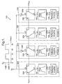
- An amplifier circuit (100) for receiving an input signal (Sin) and providing a corresponding amplified output signal (Sout), the circuit (100) characterised in that it comprises:(a) a plurality of reflection amplifiers (110, 120, 130, 140) cascaded in series along a signal path and operative to amplify the input signal (Sin) propagating in a forward direction therealong to provide the output signal (Sout); and(b) connecting means (150, 160, 170, 180, 200, 210, 220, 230) for connecting the reflection amplifiers (110, 120, 130, 140) to form the signal path and for hindering signal propagation in a reverse direction therealong, thereby counteracting spontaneous oscillation from arising within the circuit, the connecting means incorporating switching means (200, 210, 220, 230) for alternatively switching a plurality of the reflection amplifiers (110, 120, 130, 140) such that each reflection amplifier is operable to receive signals propagating in the forward direction along the path and to output the signals after amplification to the signal path to propagate further in the forward direction therealong, the reflection amplifiers (110, 120, 130, 140) incorporating signal delaying means for delaying signal propagation to and from the reflection amplifiers (110, 120, 130, 140).
- A circuit according to Claim 1 wherein the delaying means comprises a plurality of delay lines, such that a delay line is interposed between each reflection amplifier (110, 120, 130, 140) and the switching means (200, 210, 220, 230).
- A circuit according to Claim 2 wherein the delay lines are operative to provide a signal delay therethrough of a time period τ and the switching means (220, 210, 220 230) is arranged to switch alternately at a rate having an associated time period which is a multiple of the period τ.
- A circuit according to Claim 2 or 3 wherein the delay lines comprise SAW, BAW or ceramic devices.
- A circuit according to Claim 2, 3 or 4 wherein the delay lines are operative to provide bandpass signal transmission therethrough.
- A circuit according to Claim 1, 2, 3, 4 or 5 wherein the switching means comprises a series of switches (200, 210, 220, 230) cascaded in series to define the signal path, the switches being operative so that switches neighbouring one another are in mutually opposite connection states to counteract in co-operation with the delaying means signal propagation in a reverse direction along the signal path.
- An intermediate frequency strip incorporating an amplifier circuit according to any preceding claim.
- An intermediate frequency receiver incorporating an amplifier circuit according to any one of Claims 1 to 6.
- A mobile telephone incorporating an amplifier circuit according to any one of Claims 1 to 6.
- A method of amplifying an input signal (Sin) and providing a corresponding amplified output signal (Sout), the method including the steps of:(a) providing a plurality of reflection amplifiers (110, 120, 130, 140) cascaded in series along a signal path, and connecting means (150, 160, 170, 180, 200, 210, 220, 230) for connecting the reflection amplifiers (110, 120, 130, 140) to the signal path, the connecting means operative to promote signal propagation in a forward direction along the path and counteract signal propagation in a reverse direction therealong, the connecting means incorporating switching means (200, 210, 220, 230) for alternatively switching a plurality of the reflection amplifiers (110, 120, 130, 140) such that each amplifier is operable to receive signals propagating in the forward direction along the signal path and to output the signals after amplification to the signal path to propagate further in the forward direction therealong, the reflection amplifiers (110, 120, 130, 140) incorporating signal delaying means for delaying signal propagation to and from the reflection amplifiers (110, 120, 130, 140);(b) receiving the input signal (Sin) at the signal path;(c) directing the input signal through the connecting means to one of the reflection amplifiers for amplification therein to provide an amplified signal;(d) directing the amplified signal in the forward direction to another of the reflection amplifiers for further amplification therein;(e) repeating step (d) until the amplified signal reaches an output of the signal path (Sout); and(f) outputting the amplified signal as the output signal from the signal path.
Applications Claiming Priority (3)
| Application Number | Priority Date | Filing Date | Title |
|---|---|---|---|
| GB9911880 | 1999-05-22 | ||
| GBGB9911880.4A GB9911880D0 (en) | 1999-05-22 | 1999-05-22 | Amplifier circuit |
| PCT/GB2000/001893 WO2000072439A1 (en) | 1999-05-22 | 2000-05-17 | Amplifier circuit |
Publications (2)
| Publication Number | Publication Date |
|---|---|
| EP1186097A1 EP1186097A1 (en) | 2002-03-13 |
| EP1186097B1 true EP1186097B1 (en) | 2003-04-02 |
Family
ID=10853926
Family Applications (2)
| Application Number | Title | Priority Date | Filing Date |
|---|---|---|---|
| EP00931389A Expired - Lifetime EP1186097B1 (en) | 1999-05-22 | 2000-05-17 | Amplifier circuit |
| EP00931390A Expired - Lifetime EP1188231B1 (en) | 1999-05-22 | 2000-05-17 | Amplifier circuit |
Family Applications After (1)
| Application Number | Title | Priority Date | Filing Date |
|---|---|---|---|
| EP00931390A Expired - Lifetime EP1188231B1 (en) | 1999-05-22 | 2000-05-17 | Amplifier circuit |
Country Status (11)
| Country | Link |
|---|---|
| US (3) | US6799027B1 (en) |
| EP (2) | EP1186097B1 (en) |
| JP (2) | JP4498619B2 (en) |
| KR (1) | KR100849001B1 (en) |
| CN (2) | CN1365537A (en) |
| AT (2) | ATE245317T1 (en) |
| AU (2) | AU4934600A (en) |
| CA (2) | CA2371593A1 (en) |
| DE (2) | DE60001940T2 (en) |
| GB (3) | GB9911880D0 (en) |
| WO (2) | WO2000072439A1 (en) |
Families Citing this family (10)
| Publication number | Priority date | Publication date | Assignee | Title |
|---|---|---|---|---|
| GB9911880D0 (en) * | 1999-05-22 | 1999-07-21 | Marconi Electronic Syst Ltd | Amplifier circuit |
| US7623837B2 (en) * | 2004-05-10 | 2009-11-24 | Stmicroelectronics S.A. | Receiver for an integrated heterodyne communication system including BAW-type resonators |
| US7768407B2 (en) | 2007-06-22 | 2010-08-03 | Avery Dennison Corporation | Foldable RFID device interposer and method |
| US7880614B2 (en) * | 2007-09-26 | 2011-02-01 | Avery Dennison Corporation | RFID interposer with impedance matching |
| US8633821B2 (en) * | 2007-12-03 | 2014-01-21 | Avery Dennison Corporation | Dual use RFID/EAS device |
| US8847764B2 (en) | 2007-12-05 | 2014-09-30 | Avery Dennison Corporation | RFID system with distributed read structure |
| US7786868B2 (en) * | 2007-12-11 | 2010-08-31 | Avery Dennison Corporation | RFID device with multiple passive operation modes |
| KR20180120938A (en) * | 2017-04-28 | 2018-11-07 | 주식회사 에이디알에프코리아 | Amplification System for Public Safety |
| US11233482B2 (en) * | 2019-07-31 | 2022-01-25 | Skyworks Solutions, Inc. | Receiver front end for digital isolators |
| CN113437943B (en) * | 2021-08-11 | 2022-05-13 | 电子科技大学 | Passive UHF RFID tag circuit with bidirectional amplification |
Family Cites Families (32)
| Publication number | Priority date | Publication date | Assignee | Title |
|---|---|---|---|---|
| US3633134A (en) * | 1969-10-10 | 1972-01-04 | Motorola Inc | Crystal band pass filter circuit |
| US3699454A (en) * | 1970-01-30 | 1972-10-17 | Hughes Aircraft Co | Degenerate parametric amplifier receiver |
| US3646467A (en) | 1970-11-02 | 1972-02-29 | Raytheon Co | Solid-state electromagnetic energy amplifier system |
| US3663886A (en) * | 1970-12-17 | 1972-05-16 | Nasa | Parametric amplifiers with idler circuit feedback |
| FR2157933B1 (en) | 1971-10-26 | 1980-04-18 | Licentia Gmbh | |
| US3768029A (en) * | 1972-09-11 | 1973-10-23 | Rca Corp | Temperature compensation of transferred electron amplifiers |
| US4080602A (en) * | 1973-07-04 | 1978-03-21 | Takeshi Hattori | Wireless control system for a travelling toy using a single transmitting and receiving channel |
| US4150382A (en) * | 1973-09-13 | 1979-04-17 | Wisconsin Alumni Research Foundation | Non-uniform variable guided wave antennas with electronically controllable scanning |
| US3930206A (en) * | 1974-05-03 | 1975-12-30 | Troike Robert L | Broad-band amplifier using cascaded class C amplifiers |
| DE2459053C3 (en) * | 1974-12-13 | 1981-10-01 | Siemens AG, 1000 Berlin und 8000 München | FM radio relay system with RF switching |
| US4086543A (en) * | 1976-07-21 | 1978-04-25 | Canadian Patents & Development Limited | Travelling wave hybrid junction amplifier |
| JPS55105408A (en) * | 1979-02-06 | 1980-08-13 | Nec Corp | Reception frequency converting device |
| JPS55137707A (en) | 1979-04-14 | 1980-10-27 | Nec Corp | Multistage amplifier of microwave band |
| FR2435866A1 (en) * | 1979-05-16 | 1980-04-04 | Trt Telecom Radio Electr | MAINTAINED PSEUDO-WAVE ANSWER COMPRISING TWO-POSITION SWITCHES FOR RADIO FREQUENCIES |
| JPS5622813U (en) * | 1979-07-27 | 1981-02-28 | ||
| JPS59147549A (en) | 1983-02-10 | 1984-08-23 | Fujitsu Ltd | Direct repeater |
| JPS60127806A (en) | 1983-12-15 | 1985-07-08 | Toshiba Corp | Power supply start and stop device of microwave multi- stage amplifier |
| KR860001241B1 (en) * | 1984-05-10 | 1986-08-30 | 삼성반도체통신 주식회사 | Integrated circuit for driving a d.c.motor having operational modes |
| GB9002789D0 (en) * | 1990-02-08 | 1990-04-04 | Marconi Co Ltd | Circuit for reducing distortion produced by an r.f.power amplifier |
| US5170495A (en) * | 1990-10-31 | 1992-12-08 | Northern Telecom Limited | Controlling clipping in a microwave power amplifier |
| US5237288A (en) * | 1992-06-05 | 1993-08-17 | Sea, Inc. | RF power amplifier linearization |
| US5305109A (en) * | 1992-09-08 | 1994-04-19 | Samsung Electronics Co., Ltd. | Parallel untuned video if amplifiers supplied signals from TV 1st detector via respective input filters |
| GB9324534D0 (en) * | 1993-11-30 | 1994-01-19 | Marconi Gec Ltd | Circuit arrangement |
| US5493719A (en) * | 1994-07-01 | 1996-02-20 | The United States Of America As Represented By The Secretary Of The Air Force | Integrated superconductive heterodyne receiver |
| US5530402A (en) * | 1995-01-27 | 1996-06-25 | Rf Monolithics, Inc. | Single sequential amplifier circuit |
| US5862461A (en) | 1995-08-31 | 1999-01-19 | Sony Corporation | Transmitting apparatus and method of adjusting gain of signal to be transmitted, and receiving apparatus and method of adjusting gain of received signal |
| US5901347A (en) * | 1996-01-17 | 1999-05-04 | Motorola, Inc. | Fast automatic gain control circuit and method for zero intermediate frequency receivers and radiotelephone using same |
| SE510569C2 (en) * | 1996-05-31 | 1999-06-07 | Allgon Ab | Variable bandwidth repeater |
| EP0828385B1 (en) * | 1996-09-06 | 2006-06-14 | Nec Corporation | Digital amplitude modulation amplifier and television broadcasting machine |
| US6072824A (en) * | 1998-01-23 | 2000-06-06 | Adc Solitra, Inc. | Circuit arrangement for reducing intermodulation in a bandpass filter system |
| GB9808762D0 (en) | 1998-04-25 | 1998-06-24 | Marconi Gec Ltd | Modulated reflector circuit |
| GB9911880D0 (en) * | 1999-05-22 | 1999-07-21 | Marconi Electronic Syst Ltd | Amplifier circuit |
-
1999
- 1999-05-22 GB GBGB9911880.4A patent/GB9911880D0/en not_active Ceased
-
2000
- 2000-05-16 GB GB0011665A patent/GB2350957B/en not_active Revoked
- 2000-05-16 GB GB0011666A patent/GB2350958B/en not_active Revoked
- 2000-05-17 KR KR1020017014943A patent/KR100849001B1/en not_active IP Right Cessation
- 2000-05-17 EP EP00931389A patent/EP1186097B1/en not_active Expired - Lifetime
- 2000-05-17 JP JP2000620730A patent/JP4498619B2/en not_active Expired - Fee Related
- 2000-05-17 US US09/926,572 patent/US6799027B1/en not_active Ceased
- 2000-05-17 EP EP00931390A patent/EP1188231B1/en not_active Expired - Lifetime
- 2000-05-17 DE DE60001940T patent/DE60001940T2/en not_active Expired - Lifetime
- 2000-05-17 US US11/541,516 patent/USRE40900E1/en not_active Expired - Lifetime
- 2000-05-17 AT AT00931390T patent/ATE245317T1/en not_active IP Right Cessation
- 2000-05-17 US US09/926,573 patent/US6480062B1/en not_active Expired - Lifetime
- 2000-05-17 JP JP2000620731A patent/JP4498620B2/en not_active Expired - Fee Related
- 2000-05-17 AU AU49346/00A patent/AU4934600A/en not_active Abandoned
- 2000-05-17 AT AT00931389T patent/ATE236473T1/en not_active IP Right Cessation
- 2000-05-17 WO PCT/GB2000/001893 patent/WO2000072439A1/en active IP Right Grant
- 2000-05-17 CN CN00810682A patent/CN1365537A/en active Pending
- 2000-05-17 AU AU49347/00A patent/AU4934700A/en not_active Abandoned
- 2000-05-17 WO PCT/GB2000/001895 patent/WO2000072440A1/en active IP Right Grant
- 2000-05-17 CA CA002371593A patent/CA2371593A1/en not_active Abandoned
- 2000-05-17 CA CA002371595A patent/CA2371595A1/en not_active Abandoned
- 2000-05-17 CN CN00810599A patent/CN1364336A/en active Pending
- 2000-05-17 DE DE60003925T patent/DE60003925T2/en not_active Expired - Lifetime
Also Published As
| Publication number | Publication date |
|---|---|
| GB9911880D0 (en) | 1999-07-21 |
| GB2350958B (en) | 2001-08-01 |
| KR20020053033A (en) | 2002-07-04 |
| DE60003925D1 (en) | 2003-08-21 |
| US6480062B1 (en) | 2002-11-12 |
| GB2350957B (en) | 2001-08-01 |
| WO2000072440A1 (en) | 2000-11-30 |
| EP1188231A1 (en) | 2002-03-20 |
| ATE236473T1 (en) | 2003-04-15 |
| ATE245317T1 (en) | 2003-08-15 |
| CA2371595A1 (en) | 2000-11-30 |
| CN1365537A (en) | 2002-08-21 |
| US6799027B1 (en) | 2004-09-28 |
| JP4498620B2 (en) | 2010-07-07 |
| GB2350957A (en) | 2000-12-13 |
| DE60003925T2 (en) | 2004-02-05 |
| CA2371593A1 (en) | 2000-11-30 |
| EP1186097A1 (en) | 2002-03-13 |
| KR100849001B1 (en) | 2008-07-30 |
| DE60001940D1 (en) | 2003-05-08 |
| JP4498619B2 (en) | 2010-07-07 |
| DE60001940T2 (en) | 2004-01-08 |
| AU4934700A (en) | 2000-12-12 |
| EP1188231B1 (en) | 2003-07-16 |
| GB0011666D0 (en) | 2000-07-05 |
| AU4934600A (en) | 2000-12-12 |
| CN1364336A (en) | 2002-08-14 |
| USRE40900E1 (en) | 2009-09-01 |
| GB2350958A (en) | 2000-12-13 |
| WO2000072439A1 (en) | 2000-11-30 |
| JP2003500967A (en) | 2003-01-07 |
| GB0011665D0 (en) | 2000-07-05 |
| JP2003500968A (en) | 2003-01-07 |
Similar Documents
| Publication | Publication Date | Title |
|---|---|---|
| US6157253A (en) | High efficiency power amplifier circuit with wide dynamic backoff range | |
| KR100247079B1 (en) | Output-controlled power amplifier, radio communication terminal and radio communication base station | |
| JP2996170B2 (en) | Gain control circuit | |
| EP1186097B1 (en) | Amplifier circuit | |
| WO2003065599A1 (en) | Power amplification apparatus of portable terminal | |
| JPH03258126A (en) | Transmission/reception switching device | |
| JPH05347522A (en) | Automatic gain control circuit | |
| KR20020026836A (en) | A method for reducing noise generated in a power amplifier | |
| SE508415C2 (en) | High frequency circuitry for a radio receiver | |
| JP2002016448A (en) | Radio frequency amplifier circuit and receiving chain circuit | |
| JP3201885B2 (en) | Bidirectional relay amplifier | |
| JP3504514B2 (en) | High frequency amplifier | |
| JPH05304485A (en) | Receiver | |
| JPH10107738A (en) | Optical receiver | |
| JP2001102982A (en) | Repeating and amplifying device | |
| JPH06268404A (en) | High frequency signal switch | |
| JP2003259150A (en) | Amplifier with tilt circuit | |
| JP2001156560A (en) | High frequency power amplifier | |
| JPH01318416A (en) | Semiconductor amplifying circuit | |
| EP0839405A1 (en) | Error path control for feed-forward amplifier | |
| JPH05315978A (en) | Automatic gain control circuit | |
| JPH07297731A (en) | Radio transmission circuit | |
| JPS6412134B2 (en) | ||
| JP2001339316A (en) | Radio equipment |
Legal Events
| Date | Code | Title | Description |
|---|---|---|---|
| PUAI | Public reference made under article 153(3) epc to a published international application that has entered the european phase |
Free format text: ORIGINAL CODE: 0009012 |
|
| 17P | Request for examination filed |
Effective date: 20011217 |
|
| AK | Designated contracting states |
Kind code of ref document: A1 Designated state(s): AT BE CH CY DE DK ES FI FR GB GR IE IT LI LU MC NL PT SE |
|
| AX | Request for extension of the european patent |
Free format text: AL;LT;LV;MK;RO;SI |
|
| GRAH | Despatch of communication of intention to grant a patent |
Free format text: ORIGINAL CODE: EPIDOS IGRA |
|
| GRAH | Despatch of communication of intention to grant a patent |
Free format text: ORIGINAL CODE: EPIDOS IGRA |
|
| GRAA | (expected) grant |
Free format text: ORIGINAL CODE: 0009210 |
|
| AK | Designated contracting states |
Designated state(s): AT BE CH CY DE DK ES FI FR GB GR IE IT LI LU MC NL PT SE |
|
| PG25 | Lapsed in a contracting state [announced via postgrant information from national office to epo] |
Ref country code: AT Free format text: LAPSE BECAUSE OF FAILURE TO SUBMIT A TRANSLATION OF THE DESCRIPTION OR TO PAY THE FEE WITHIN THE PRESCRIBED TIME-LIMIT Effective date: 20030402 Ref country code: LI Free format text: LAPSE BECAUSE OF FAILURE TO SUBMIT A TRANSLATION OF THE DESCRIPTION OR TO PAY THE FEE WITHIN THE PRESCRIBED TIME-LIMIT Effective date: 20030402 Ref country code: BE Free format text: LAPSE BECAUSE OF FAILURE TO SUBMIT A TRANSLATION OF THE DESCRIPTION OR TO PAY THE FEE WITHIN THE PRESCRIBED TIME-LIMIT Effective date: 20030402 Ref country code: CH Free format text: LAPSE BECAUSE OF FAILURE TO SUBMIT A TRANSLATION OF THE DESCRIPTION OR TO PAY THE FEE WITHIN THE PRESCRIBED TIME-LIMIT Effective date: 20030402 |
|
| RAP1 | Party data changed (applicant data changed or rights of an application transferred) |
Owner name: A.B. DICK HOLDINGS LIMITED |
|
| REG | Reference to a national code |
Ref country code: GB Ref legal event code: FG4D |
|
| REG | Reference to a national code |
Ref country code: CH Ref legal event code: EP |
|
| REG | Reference to a national code |
Ref country code: IE Ref legal event code: FG4D |
|
| REF | Corresponds to: |
Ref document number: 60001940 Country of ref document: DE Date of ref document: 20030508 Kind code of ref document: P |
|
| PGFP | Annual fee paid to national office [announced via postgrant information from national office to epo] |
Ref country code: FI Payment date: 20030515 Year of fee payment: 4 |
|
| PG25 | Lapsed in a contracting state [announced via postgrant information from national office to epo] |
Ref country code: LU Free format text: LAPSE BECAUSE OF NON-PAYMENT OF DUE FEES Effective date: 20030517 Ref country code: CY Free format text: LAPSE BECAUSE OF FAILURE TO SUBMIT A TRANSLATION OF THE DESCRIPTION OR TO PAY THE FEE WITHIN THE PRESCRIBED TIME-LIMIT Effective date: 20030517 |
|
| PG25 | Lapsed in a contracting state [announced via postgrant information from national office to epo] |
Ref country code: IE Free format text: LAPSE BECAUSE OF NON-PAYMENT OF DUE FEES Effective date: 20030519 |
|
| PG25 | Lapsed in a contracting state [announced via postgrant information from national office to epo] |
Ref country code: MC Free format text: LAPSE BECAUSE OF NON-PAYMENT OF DUE FEES Effective date: 20030531 |
|
| PG25 | Lapsed in a contracting state [announced via postgrant information from national office to epo] |
Ref country code: DK Free format text: LAPSE BECAUSE OF FAILURE TO SUBMIT A TRANSLATION OF THE DESCRIPTION OR TO PAY THE FEE WITHIN THE PRESCRIBED TIME-LIMIT Effective date: 20030702 Ref country code: PT Free format text: LAPSE BECAUSE OF FAILURE TO SUBMIT A TRANSLATION OF THE DESCRIPTION OR TO PAY THE FEE WITHIN THE PRESCRIBED TIME-LIMIT Effective date: 20030702 Ref country code: GR Free format text: LAPSE BECAUSE OF FAILURE TO SUBMIT A TRANSLATION OF THE DESCRIPTION OR TO PAY THE FEE WITHIN THE PRESCRIBED TIME-LIMIT Effective date: 20030702 |
|
| REG | Reference to a national code |
Ref country code: SE Ref legal event code: TRGR |
|
| REG | Reference to a national code |
Ref country code: GB Ref legal event code: 732E |
|
| ET | Fr: translation filed | ||
| LTIE | Lt: invalidation of european patent or patent extension |
Effective date: 20030402 |
|
| REG | Reference to a national code |
Ref country code: CH Ref legal event code: PL |
|
| PG25 | Lapsed in a contracting state [announced via postgrant information from national office to epo] |
Ref country code: ES Free format text: LAPSE BECAUSE OF FAILURE TO SUBMIT A TRANSLATION OF THE DESCRIPTION OR TO PAY THE FEE WITHIN THE PRESCRIBED TIME-LIMIT Effective date: 20031030 |
|
| PLBE | No opposition filed within time limit |
Free format text: ORIGINAL CODE: 0009261 |
|
| STAA | Information on the status of an ep patent application or granted ep patent |
Free format text: STATUS: NO OPPOSITION FILED WITHIN TIME LIMIT |
|
| REG | Reference to a national code |
Ref country code: IE Ref legal event code: MM4A |
|
| 26N | No opposition filed |
Effective date: 20040105 |
|
| PG25 | Lapsed in a contracting state [announced via postgrant information from national office to epo] |
Ref country code: FI Free format text: LAPSE BECAUSE OF NON-PAYMENT OF DUE FEES Effective date: 20040517 |
|
| PG25 | Lapsed in a contracting state [announced via postgrant information from national office to epo] |
Ref country code: SE Free format text: LAPSE BECAUSE OF NON-PAYMENT OF DUE FEES Effective date: 20040518 |
|
| NLS | Nl: assignments of ep-patents |
Owner name: MARCONI UK INTELLECTUAL PROPERTY LTD |
|
| EUG | Se: european patent has lapsed | ||
| REG | Reference to a national code |
Ref country code: FR Ref legal event code: CA Ref country code: FR Ref legal event code: TP |
|
| REG | Reference to a national code |
Ref country code: GB Ref legal event code: 732E |
|
| PGFP | Annual fee paid to national office [announced via postgrant information from national office to epo] |
Ref country code: NL Payment date: 20050605 Year of fee payment: 7 |
|
| REG | Reference to a national code |
Ref country code: FR Ref legal event code: TP |
|
| PGFP | Annual fee paid to national office [announced via postgrant information from national office to epo] |
Ref country code: IT Payment date: 20060531 Year of fee payment: 7 |
|
| PG25 | Lapsed in a contracting state [announced via postgrant information from national office to epo] |
Ref country code: NL Free format text: LAPSE BECAUSE OF NON-PAYMENT OF DUE FEES Effective date: 20071201 |
|
| PGFP | Annual fee paid to national office [announced via postgrant information from national office to epo] |
Ref country code: SE Payment date: 20030507 Year of fee payment: 4 |
|
| NLV4 | Nl: lapsed or anulled due to non-payment of the annual fee |
Effective date: 20071201 |
|
| PG25 | Lapsed in a contracting state [announced via postgrant information from national office to epo] |
Ref country code: IT Free format text: LAPSE BECAUSE OF NON-PAYMENT OF DUE FEES Effective date: 20070517 |
|
| REG | Reference to a national code |
Ref country code: FR Ref legal event code: PLFP Year of fee payment: 17 |
|
| PGFP | Annual fee paid to national office [announced via postgrant information from national office to epo] |
Ref country code: DE Payment date: 20160524 Year of fee payment: 17 Ref country code: GB Payment date: 20160426 Year of fee payment: 17 |
|
| PGFP | Annual fee paid to national office [announced via postgrant information from national office to epo] |
Ref country code: FR Payment date: 20160428 Year of fee payment: 17 |
|
| REG | Reference to a national code |
Ref country code: DE Ref legal event code: R119 Ref document number: 60001940 Country of ref document: DE |
|
| GBPC | Gb: european patent ceased through non-payment of renewal fee |
Effective date: 20170517 |
|
| REG | Reference to a national code |
Ref country code: FR Ref legal event code: ST Effective date: 20180131 |
|
| PG25 | Lapsed in a contracting state [announced via postgrant information from national office to epo] |
Ref country code: DE Free format text: LAPSE BECAUSE OF NON-PAYMENT OF DUE FEES Effective date: 20171201 Ref country code: GB Free format text: LAPSE BECAUSE OF NON-PAYMENT OF DUE FEES Effective date: 20170517 |
|
| PG25 | Lapsed in a contracting state [announced via postgrant information from national office to epo] |
Ref country code: FR Free format text: LAPSE BECAUSE OF NON-PAYMENT OF DUE FEES Effective date: 20170531 |