Technical Field
-
The present invention relates to a display device for an
electronic apparatus comprising a solar cell, for example, an
electronic apparatus such as a watch, an electronic calculator,
a radio, a battery charger, and more particularly the watch.
Background Art
-
With reference to Fig. 26, a conventional example of a
structure of a watch having a solar cell 305 will be described
in detail. Fig. 26(a) is a front view showing the inside of
a watch case seen from above and Fig. 26B is a schematic sectional
view showing the inside of the watch case.
-
As shown in Fig. 26, when light is incident on a solar
display board 301 of a watch from the outside, the light is
transmitted through the solar display board 301 to reach the
solar cell 305. Then, the solar cell 305 is such a mechanism
that an optical energy is converted into an electric energy which
is charged into a battery or capacitor referred to as a secondary
battery which is provided in a module 307 and can store electricity,
and simultaneously, the module 307 is conducted so that a minute
hand 301 and an hour hand 309 which are fixed to a central shaft
308 are moved. In this case, the solar display board 301 is
positioned between the minute hand 310 and hour hand 309 and
the solar cell 305. Moreover, the module 307 indicates a driving
portion in the watch.
-
In recent years, the power generation efficiency of the
solar cell has been enhanced, the power consumption of a module
has been reduced, and furthermore, a battery performance has
been improved. Consequently, even if the external shape of a
solar cell is much smaller than ever, a minute hand and an hour
hand can be driven.
-
On the other hand, the degree of freedom has been
increasingly required for the external shape of a watch case
depending on the diversification of the design of the watch.
A middle frame 306 is positioned on the outside of the solar
cell 305 and the module 307 so that the degree of freedom can
be enhanced in respect of the design of the external shape of
the watch.
-
As shown in Figs. 26(a) and (b), the solar cell 305 and
the module 307 are fixed through the middle frame 306 to an outer
case which is not shown. Moreover, the minute hand 310 and the
hour hand 309 are bonded to the central shaft 308 extended from
the module 307 and are rotated through driving force applied
from the module 307. Furthermore, the solar display board 301
is provided to cover the solar cell 305 and the middle frame
306.
-
The middle frame 306 is provided with a hook mechanism
in order to fix the module 307 to which the solar cell 305 is
fastened, which is not shown. When the module 307 is fitted
in the middle frame 306, the solar cell 305 and the module 307
are fixed to the middle frame 306 and are accommodated in the
outer case and thus fixed therein.
-
The solar cell 305 has two kinds of substrates, that is,
substrates formed of a glass and a resin. For both of them,
the solar cell itself has a small thickness. Furthermore, there
is a possibility that the substrate formed of a glass might be
chipped through a stress such as a shock during or after assembly.
The substrate formed of a resin might be deformed by a stress
thereof during bonding. For a method of fixation to the watch
case, therefore, the solar cell 305 and the middle frame 306
are not fixed but the module 307 and the middle frame 306 are
fixed. In the case of the substrate formed of a resin, a metal
plate may be provided on the lower face of the solar cell 305
in order to enhance the reliability of rigidity and electrical
connection.
-
Furthermore, in the case in which the solar display board
301 comes in contact with the solar cell 305, the power generation
efficiency of the solar cell 305 might be reduced due to a flaw
or the like. Therefore, the middle frame 306 also has the
function of preventing the reduction of the power generation.
When the solar display board 301 is superposed on the solar cell
305, the middle frame 306 is protruded slightly upward from the
upper face of the solar cell 305 such that the middle frame 306
comes in contact with the solar display board 301 earlier than
the solar cell 305.
-
Moreover, in the case in which the module 307 having the
solar cell 305 fixed thereto is to be incorporated into the middle
frame 306, the incorporation can easily be carried out easily
and productivity can be enhanced if the external shape of the
solar cell 305 is coincident with that of the module 307 as shown.
As described above in detail, the middle frame in watch parts
is a member for playing an important role.
-
As shown in Fig. 26 (a), a boundary line 303 between the
solar cell 305 and the middle frame 306 usually requires a
clearance for a watch assembling work and the clearance is seen
to be black through the solar display board 301. Moreover, a
plastic material is often used for the middle frame 306 in
consideration of easiness of molding, a cost, a shock absorption
and the like, and the middle frame 306 is fabricated through
injection molding to correspond to various outer cases.
Therefore, a gate track 304 is formed on an upper face of the
middle frame 306 due to the injection molding and the gate track
304 is also seen through the solar display board 301. Furthermore,
in the case in which a solar cell is divided into some elements
to maintain a predetermined voltage and current, a refractive
index of light is varied depending on a difference in a material
between a cell portion and a dividing line portion and a solar
cell element dividing line 302 is also seen through the solar
display board 301.
-
According to the knowledge of the present inventors, such
a phenomenon remarkably presents itself when the solar display
board 301 is black or blue. Fig. 26 shows an example in which
the solar cell element dividing line 302 has a cross-shape and
the boundary line 303 between the solar cell 305 and the middle
frame 306 has the shape of a black ring on the boundary between
a slant line portion and a dotted portion.
-
For a technique for seeing such a solar cell element
dividing line with difficulty, a method disclosed in Japanese
Patent Publication No. Hei 5-38464 has conventionally been
proposed.
-
In the Japanese Patent Publication No. Hei 5-38464, only
a color diffusing board is provided between the solar display
board 301 and the solar cell 305. However, the diffusing board
has the function of diffusing light. Therefore, the boundary
line 303 between the solar cell 305 and the middle frame, the
gate track 304 generated through the injection molding of the
middle frame, and furthermore, the solar cell element dividing
line 302 are seen with difficulty. As a result, they are
necessarily seen to be white so that the tone of the solar display
board 301 provided thereabove is affected.
-
According to an experiment carried out by the present
inventors, if only the color diffusing board is provided between
the solar display board 301 and the solar cell 305, a black solar
display board is seen to be gray, which is not preferable in
respect of design. Moreover, a white solar display board has
diffusion effects by itself. Therefore, even if the diffusing
board is not used, there is not such a phenomenon that the boundary
line 303 between the solar cell 305 and the middle frame 306,
the gate track 304 generated through the injection molding of
the middle frame 306, and furthermore, the solar cell element
dividing line 302 are seen through the solar display board 301.
Therefore, it is not necessary to provide the diffusing board
as in the Japanese Patent Publication No. Hei 5-38464.
-
Usually, various designs are given through the solar
display board 301. If there is such a phenomenon that the
boundary line 303, the gate track 304 and the solar cell element
dividing line 302 are seen as described above, the quality of
design of a watch is adversely affected. More specifically,
in this case, a decoration or the like should be given to a part
of the solar display board 301 or the whole surface thereof in
order to hide the above-mentioned phenomenon. Therefore, the
design for the solar display board 301 is restricted so that
a feeling of high quality for a watch is eliminated.
-
In the three phenomena adversely affecting the design
quality as described above, the solar cell element dividing line
302 can be considerably improved by giving a protective coat
formed of an epoxy resin which has SiO2 particulates distributed
therein over the whole surface of the solar cell 305. Moreover,
there is a possibility that the gate track 304 generated during
the injection molding of the middle frame 306 can also be improved
by changing a gate position. However, the boundary line 303
between the solar cell 305 and the middle frame 306, that is,
the clearance cannot be avoided for the watch assembling work
and is the most harmful and measures are taken with difficulty.
-
In the experiment carried out by the present inventors,
the colors of black and blue solar display boards are caused
to be deeper, a feeling of high quality can be obtained for goods
by the deeper colors, and furthermore, it is possible to eliminate
such a drawback that the observation through the solar display
board described above is caused. However, transmitted light
does not fully reach the solar cell itself so that the power
generation efficiency is reduced and the operation of the watch
is stopped.
-
Moreover, when the tone of the middle frame is adapted
to that of the solar cell, it is possible to eliminate such a
drawback that the observation through the solar display board
described above is caused. However, the boundary line between
the solar cell and the middle frame is seen so that the drawback
cannot be eliminated completely. Furthermore, when a white
paint is thinly applied to the solar cell side of the blue solar
display board having a blue resin kneaded therein, it is possible
to eliminate such a phenomenon that the boundary line 303 between
the solar cell 305 and the middle frame 306, the gate track 304
generated through the injection molding of the middle frame 306,
and furthermore, the solar cell element dividing line 302 are
seen through the solar display board 301. However, the depth
of the color of the solar display board 301 is eliminated by
the diffusing function of the white paint so that the feeling
of high quality for the single solar display board disappears.
In other words, the formation of a diffusion layer cannot obtain
sufficient effects.
-
In a display board such as a watch dial, various coloring
and patterns are applied to the surface or back of the display
board or both of them in order to give a feeling of high quality
(added value) in some cases. The coloring is carried out by
printing the surface of a material to be the display board or
manufacturing the display board from a resin containing a pigment,
for example. In the case of a metallic display board, moreover,
the pattern on the surface thereof is formed through etching,
a mat processing or the like. In the case of a display board
formed of a resin, a pattern is formed by injection molding the
resin in a mold having the pattern formed therein.
-
However, the above-mentioned display boards are not
satisfactory in respect of the depth of a pattern, a
three-dimensional effect and the like.
-
In consideration of such circumstances, it is an object
of the present invention to provide a display device for an
electronic apparatus comprising a solar cell and a middle frame
for fixing the solar cell and a module to an outer case in which
necessary and sufficient light can be caused to reach the solar
cell, a feeling of high quality can be given, and furthermore,
it is possible to increase a variation in design in which a
decorative property is great and the depth of a pattern and a
three-dimensional effect are excellent.
Disclosure of the Invention
-
The present invention has been made to solve the problems
of the conventional art described above and to achieve the
above-mentioned object and provides a display device for an
electronic apparatus comprising a solar cell, wherein a circular
polarizing plate for transmitting light is provided on the front
side of the solar cell in a direction of incidence of light.
-
In a circular polarizing plate constituted by a linear
polarizing plate and a phase difference plate, the linear
polarizing plate and the phase difference plate are provided
in this order in a direction of incidence of light. Consequently,
light reflected by a solar cell surface can be blocked, a boundary
line between the solar cell and the middle frame, a gate track
generated through injection molding of the middle frame, and
a solar cell element dividing line cannot be seen through the
circular polarizing plate.
-
Consequently, the tone of the solar display board is not
affected. Moreover, it is not necessary to hide the three
drawbacks through a stripe-shaped pattern or the like. Thus,
a variation in design of the solar display board can be increased.
Furthermore, a solar display board having a deep color can be
used so that a feeling of high quality can visually be obtained
as goods. By directly giving marking such as a numeral to the
linear polarizing plate by means of printing or the like, the
function of the solar display board can also be given to the
linear polarizing plate itself.
-
Moreover, the present invention is characterized in that
the surface of the circular polarizing plate is provided with
a solar display board constituted by a resin substrate having
a pattern, an inorganic substrate having a pattern or a decorating
thin film member or a combination thereof.
-
Therefore, a decorative property is great, the pattern
becomes rich and an excellent three-dimensional effect can be
obtained. Through a combination of two or more patterns or two
or more materials, moreover, it is possible to manufacture a
display board having a better feeling of beauty than ever. Thus,
a design variation can be increased.
-
By such a structure, it is possible to provide a display
device for an electronic apparatus comprising a solar cell
capable of maintaining the necessary and sufficient power
generation efficiency of the solar cell, giving a feeling of
high quality and increasing a variation in design.
Brief Description of the Drawings
-
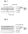
- Fig. 1 is a schematic sectional view showing the inside
of a watch case according to a first embodiment of the present
invention,
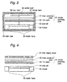
- Fig. 2 is a schematic sectional view showing the inside
of a watch case according to a second embodiment of the present
invention,
- Fig. 3 is a schematic sectional view showing the inside
of a watch case according to a third embodiment of the present
invention,
- Fig. 4 is a schematic sectional view showing the inside
of a watch case according to a fourth embodiment of the present
invention,
- Fig. 5 is a schematic sectional view showing the inside
of a watch case according to a fifth embodiment of the present
invention,
- Fig. 6 is a schematic sectional view showing the inside
of a watch case according to a sixth embodiment of the present
invention.
- Fig. 7 is a schematic sectional view showing the inside
of a watch case according to a seventh embodiment of the present
invention,
- Fig. 8 is a schematic sectional view showing the inside
of a watch case according to an eighth embodiment of the present
invention,
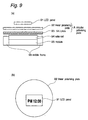
- Fig. 9 shows the inside of a watch case according to a
ninth embodiment of the present invention, Fig. 9(a) being a
schematic sectional view showing the inside of the watch case
and Fig. 9(b) being a front view showing the inside of the watch
case seen from above,
- Fig. 10 is a schematic sectional view showing the inside
of a watch case according to a tenth embodiment of the present
invention,
- Fig. 11 is a schematic sectional view showing the inside
of a watch case according to an eleventh embodiment of the present
invention,
- Fig. 12 is a schematic sectional view showing the inside
of a watch case according to a twelfth embodiment of the present
invention,
- Fig. 13 is a schematic sectional view showing the inside
of a watch case according to a thirteenth embodiment of the present
invention,
- Fig. 14 is a partially enlarged sectional view showing
a solar display board according to the thirteenth embodiment
of the present invention,
- Fig. 15 is a schematic view showing the steps of a method
of manufacturing a resin substrate having a pattern according
to the present invention,
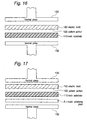
- Fig. 16 is a schematic view showing a method of forming
the resin substrate having a pattern through a thermal press
according to the present invention,
- Fig. 17 is a schematic view showing another method of
forming the resin substrate having a pattern through a thermal
press according to the present invention,
- Fig. 18 is a partially enlarged sectional view showing
a solar display board according to a fourteenth embodiment of
the present invention,
- Fig. 19 is a partially enlarged sectional view showing
a solar display board according to a fifteenth embodiment of
the present invention,
- Fig. 20 is a partially enlarged sectional view showing
a solar display board according to a sixteenth embodiment of
the present invention,
- Fig. 21 is a partially enlarged sectional view showing
a solar display board according to a seventeenth embodiment of
the present invention,
- Fig. 22 is a partially enlarged sectional view showing
a solar display board according to an eighteenth embodiment of
the present invention,
- Fig. 23 is a partially enlarged sectional view showing
a solar display board according to a nineteenth embodiment of
the present invention,
- Fig. 24 is a partially enlarged sectional view showing
a solar display board according to a twentieth embodiment of
the present invention,
- Fig. 25 is a partially enlarged sectional view showing
a solar display board according to a twenty-first embodiment
of the present invention,
- Fig. 26 shows the state of the inside of a watch case
according to a conventional example, Fig. 26(a) being a front
view showing the inside of the watch case seen from above and
Fig. 26(b) being a schematic sectional view showing the inside
of the watch case,
- Fig. 27 is a perspective view showing the principle of
an operation according to the present invention,
- Fig. 28 is a chart in which light emitted from a phase
difference board is divided into x and y directions according
to the present invention, and
- Fig. 29 is an XY table diagram showing a direction of an
oscillation of the light emitted from the phase difference board
according to the present invention.
-
Best Mode for Carrying Out the Invention
-
Embodiments of the present invention will be described
below.
-
First of all, the function of a circular polarizing plate
will be described with reference to Figs. 27 to 29.
-
The circular polarizing plate is usually fabricated by
bonding a linear polarizing plate 111 formed of a film material
to a 1/4λ plate 112 formed of a film material with an adhesive
layer. As a matter of course, if the circular polarizing plate
has the circular polarizing function, other structures and
members may be used. Moreover, the linear polarizing plate may
have such a structure that a polyvinyl alcohol thin film absorbing
iodine is extended in one direction and molecules are arranged
in parallel and are sandwiched with acetylbutyl cellulose.
Furthermore, a lens or lens group for collecting light in one
direction may be used. Since mirror reflection can be suppressed,
the linear polarizing plate is used for improving a contrast
or lessening the fatigue of eyes.
-
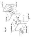
The linear polarizing plate 111 has an absorption type
or a reflection type. An absorption axis or a reflection axis
is present orthogonally to a transmission axis. When natural
light for oscillation in every direction is incident on the linear
polarizing plate 111 as shown in Fig. 27, only light in the same
oscillating direction as the transmission axis is transmitted.
In the absorption type, the light incident on the linear
polarizing plate, 111 is absorbed in the polarizing plate.
Moreover, the reflection type has the function of reflecting
the light incident on the linear polarizing plate 111 from a
surface of the polarizing plate.
-
The embodiments according to the present invention will
be described by using an absorption type linear polarizing plate
and a 1/4λ plate as the linear polarizing plate and the phase
difference plate if special description is not given.
-
The transmitted light polarized in one direction is
incident at an angle of 45° with respect to a delay axis of the
phase difference plate. In this case, the phase difference plate
represents the 1/4λ plate 112, and divides the light incident
at 45° into x and y directions for convenience and regards both
maximum amplitudes as 1 as shown in Fig. 28. An axis of abscissa
indicates an angle and an axis of ordinate indicates an amplitude,
and the relationship between a wavelength and a phase is such
that one wavelength is 360° (λ). If the delay axis of the phase
difference plate is set to the y direction, the presence of the
phase difference plate causes the light transmitted through the
phase difference plate to be delayed by a 1/4λ phase in only
the y direction.
-
The case in which the light advances by 3/4 wavelength
through the 1/4λ plate 112 will be supposed. The light is not
delayed in the x direction and is delayed by 1/4λ in the y
direction as shown in a solid line from a waveform shown in a
one-dotted chain line. Therefore, a point A (-1, 0) is obtained
in Figs. 28 and 29. Moreover, when the light further advances
by 1/4λ, a point B (0, 1) is obtained in Figs. 28 and 29 in
the same manner.
-
When a time further passes as shown in Fig. 29, the light
advances from a point C (1, 0) to a point D (0, -1) in the same
manner. Therefore, the light passing through the 1/4λ plate
112 is converted from linear polarized light into circular
polarized light as shown in Figs. 27 and 29.
-
The light thus circularly polarized is reflected by the
surfaces of a middle frame 113 and a solar cell 114, and is incident
on the 1/4λ plate 112 again reversely to a direction of advance
as shown in Fig. 27. In the same manner as described above,
the light is converted into light having an oscillation plane
in a direction perpendicular to the direction of incidence on
the 1/4λ plate 112 and the light thus obtained is vertical to
the transmission axis of the linear polarizing plate 111.
Therefore, the light cannot pass through the linear polarizing
plate 111 so that reflected light is blocked.
-
The linear polarizing plate 111 and the 1/4λ plate 112
are combined to constitute a circular polarizing plate.
-
In this case, it has been known that the incident light
is reflected by approximately several % per boundary surface
if the boundary surfaces having different refractive indices
are generally present. In the case of air and a glass, the
incident light is reflected by approximately 4 %. Therefore,
it is preferable that the number of boundary surfaces should
be decreased as greatly as possible. Accordingly, it is
preferable that the linear polarizing plate 111 and the 1/4
λ plate 112 should be stacked in a close contact state or should
be bonded with an adhesive or a glue.
-
While the linear polarizing plate 111, the 1/4λ plate
112 and the middle frame 113 are square-shaped and the solar
cell 114 is circular in Fig. 27, various other shapes may be
used corresponding to design.
(First Embodiment)
-
The explanation of function of circular polarizing has
been completed and a first embodiment will be described below
in detail with reference to Fig. 1.
-
As shown in Fig. 1, a watch having a solar cell comprises
a solar cell 13 electrically connected to a module 14, and a
minute hand 17 and an hour hand 16 which are fixed to a central
shaft 15. A circular polarizing plate A including a linear
polarizing plate 11 and a 1/4λ plate 12 is provided between
the hands 16 and 17 and the solar cell 13.
-
With such a structure, a solar cell element dividing line
of the solar cell 13 cannot be seen through the circular polarizing
plate constituted by the linear polarizing plate 11 and the 1/4
λ plate 12. Moreover, since reflected light is eliminated,
the color of the surface of the linear polarizing plate 11 is
deepened so that a feeling of high quality can be obtained as
goods.
-
In the present embodiment, marking such as a numeral is
directly given to the linear polarizing plate 11 by means of
printing to provide a function as a solar display board.
-
Moreover, it is desirable that the circular polarizing
plate A constituted by the linear polarizing plate 11 and the
1/4λ plate 12 should have a plane direction positioned by an
outer case which is not shown in respect of a watch assembling
work. In the following embodiments, since effects are not
affected, the description of the minute and hour hands will be
omitted if there is no special condition.
-
In the same manner as in the following embodiments, while
components are shown to be separated from each other for
convenience of description in the drawings, they are actually
incorporated in a close contact state, for example, properly
in a state of adhesion, bonding and welding with an adhesive,
a glue or the like.
(Second Embodiment)
-
As shown in Fig. 2, a circular polarizing plate A including
a linear polarizing plate 22 and a 1/4λ plate 23 is provided
between a solar cell 24 and a solar display board 21 having a
light transmittance.
-
Consequently, a solar cell element dividing line of the
solar cell 24 cannot be seen through the solar display board
21 so that a variation in design of the solar display board 21
is increased. Furthermore, the color of the solar display board
21 is deepened so that a feeling of high quality can be obtained
as goods.
-
In a work for assembling a watch, first of all, a module
25 is fabricated and the external shapes of the solar display
board 21, the solar cell 24, the linear polarizing plate 22 and
the 1/4λ plate 23 are simultaneously processed through press
molding or the like and they are superposed with a structure
shown in Fig. 2 in an outer case which is not shown so that a
finished watch is obtained. Accordingly, it is desirable that
the circular polarizing plate constituted by the solar display
board 21, the solar cell 24, the linear polarizing plate 22 and
the 1/4λ plate 23 should have the same external shapes.
(Third Embodiment)
-
In the present embodiment, Fig. 3 shows a structure of
a watch in which a module 34 having a solar cell 33 is fixed
into an outer case 39 through a middle frame 35.
-
A circular polarizing plate A constituted by a linear
polarizing plate 31 and a 1/4λ plate 32 is provided above the
middle frame 35 between a minute hand 37 and an hour hand 36
which are fixed to a central shaft 38 and the solar cell 33.
-
By such a structure, a boundary line between the solar
cell 33 and the middle frame 35, a gate track generated through
injection molding of the middle frame 35, and furthermore, a
solar cell element dividing line of the solar cell 33 cannot
be seen through the circular polarizing plate A constituted by
the linear polarizing plate 31 and the 1/4λ plate 32.
-
Moreover, it is desirable that the circular polarizing
plate A should be provided to cover the solar cell 33 and the
middle frame 35 as shown.
-
Since reflected light is eliminated, the color of the
surface of the linear polarizing plate 31 is deepened so that
a feeling of high quality can be obtained as goods. In the present
embodiment, marking such as a numeral is directly given to the
linear polarizing plate 31 by means of printing to provide a
function as a solar display board. Moreover, the middle frame
35 is provided. Therefore, various external shapes of the watch
can be obtained in respect of design. In the following
embodiments, since effects are not affected, the description
of the outer case will be omitted.
(Fourth Embodiment)
-
Also in the present embodiment, Fig. 4 shows a structure
of a watch in which a module 45 having a solar cell 44 is fixed
through a middle frame 46 into an outer case which is not shown.
-
In the present embodiment, a circular polarizing plate
A constituted by a linear polarizing plate 42 and a 1/4λ plate
43 is provided between the middle frame 46 and a solar display
board 41.
-
By such a structure, a boundary line between the solar
cell 44 and the middle frame 46, a gate track generated through
injection molding of the middle frame 46, and furthermore, a
solar cell element dividing line of the solar cell 44 cannot
be seen through the solar display board 41 so that a variation
in design of the solar display board 41 can be increased.
Furthermore, the color of the solar display board 41 is deepened
so that a feeling of high quality can be obtained as goods.
Moreover, the middle frame 46 is provided. Therefore, various
external shapes of the watch can be obtained in respect of design.
-
In the present embodiment, furthermore, a color display
board including a dye, a pigment and the like is used for the
solar display board 41, for example. Therefore, although a tone
has only a black color in the third embodiment, the display board
can have colors. Thus, it is apparent that practical use can
be enhanced considerably in respect of the design.
-
Moreover, it is desirable that the circular polarizing
plate A constituted by the linear polarizing plate 42 and the
1/4λ plate 43, the middle frame 46 and the solar display board
41 should have the same external shapes in respect of an assembling
work.
(Fifth Embodiment)
-
Also in the present embodiment, Fig. 5 shows a structure
of a watch in which a module 56 having a solar cell 55 is fixed
through a middle frame 57 into an outer case which is not shown.
-
In the present embodiment, a circular polarizing plate
B having a linear polarizing plate 52, a 1/4λ plate 53 and a
1/2λ plate 54 stacked is used. The circular polarizing plate
B is provided between the middle frame 57 and a solar display
board 51.
-
With such a structure, the same effects as those in the
fourth embodiment can be obtained. It has been known that the
provision of the 1/2λ plate 54 can enlarge a wavelength region
in which light can be blocked and a wideband type circular
polarizing plate can be obtained. In the same manner as the
1/4λ plate, the 1/2λ plate includes a delay axis and has the
function of delaying light incident in that direction by 1/2
λ.
(Sixth Embodiment)
-
As shown in Fig. 6, a solar display board 61, a linear
polarizing plate 62 and a 1/4λ plate 63 are bonded through an
adhesive layer 68 and are then pressurized and molded. Thus,
a circular polarizing.plate integral type solar display board
C is fabricated.
-
The circular polarizing plate integral type solar display
board C is provided above a solar cell 64 having a diffusion
layer 67 preformed on an upper surface thereof.
-
Also in this case, similarly, a boundary line between the
solar cell 64 and a middle frame 66, a gate track generated through
injection molding of the middle frame 66, and furthermore, a
solar cell element dividing line of the solar cell 64 cannot
be seen through the solar display board 61. As a result, a
variation in design of the solar display board 61 can be increased.
Furthermore, the color of the solar display board 61 is deepened
so that a feeling of high quality can be obtained as goods.
Moreover, the middle frame 66 is provided. Therefore, various
external shapes of the watch can be obtained in respect of design.
-
In general, it has been known that incident light is
reflected by approximately several % for each of boundary
surfaces having different refractive indices. In the case of
air and a glass, the incident light is reflected by approximately
4 %. Therefore, it is preferable that the number of boundary
surfaces should be decreased as greatly as possible. By
application to the present embodiment, when two film materials,
that is, the linear polarizing'plate 62 and the 1/4λ plate 63
are inserted between the solar display board 61 and the solar
cell 64 having the diffusion layer 67 formed thereon, the number
of boundary surfaces is increased through the insertion of the
films so that light transmitted to the solar cell 64 is decreased.
-
However, when the solar display board 61 and the linear
polarizing plate 62, and the linear polarizing plate 62 and the
1/4 λ plate 63 are bonded through an adhesive layer 68
respectively as in the present embodiment, the number of boundary
surfaces is decreased from 7 to 3. As a result, the light
transmitted to the solar cell 64 can be more enhanced and a power
generation efficiency can be more improved as compared with the
case in which the adhesive layer 68 is not provided.
-
In order to carry out accommodation in an outer case which
is not shown, moreover, an external shape processing is required
and a perforation processing for penetrating with a central shaft
which is not shown is also required. If three layers are bonded
by adhesive layers, the processing is carried out only once so
that the steps can be simplified and a cost can be reduced. As
compared with the case in which the three layers are processed
separately, furthermore, it is possible to prevent a shift when
the three layers are bonded. Consequently, the quality of design
can also be enhanced.
-
Furthermore, referring to a work for assembling a watch
according to the present embodiment, the diffusion layer 67 is
first formed on the surface of the solar cell 64, is bonded to
a module 65 and is then fitted in the middle frame 66. At the
same time, the solar display board 61, the linear polarizing
plate 62 and the 1/4λ plate 63 are bonded together through the
adhesive layer 68, and the external shape and perforation
processings are then carried out through a press or the like.
As shown, subsequently, they are superposed on an outer case
which is not shown. Thus, a finished watch is obtained.
-
In the present embodiment, since the solar display board
61, the linear polarizing plate 62 and the 1/4λ plate 63 are
bonded through the adhesive layer 68, they can be treated as
one member. Thus, the work for assembling a watch can be carried
out most easily in the embodiments.
(Seventh Embodiment)
-
As shown in Fig. 7, a solar display board 71, a linear
polarizing plate 72, a 1/4λ plate 73, a solar cell 74 and a
middle frame 76 are stacked as shown and are bonded with an adhesive
layer 77.
-
Also in this case, in the same manner as in the sixth
embodiment, a boundary line between the solar cell 74 and the
middle frame 76, a gate track generated through injection molding
of the middle frame 76, and furthermore, a solar cell element
dividing line of the solar cell 74 cannot be seen through the
solar display board 71 so that a variation in design of the solar
display board 71 can be increased.
-
Furthermore, the color of the solar display board 71 is
deepened so that a feeling of high quality can be obtained as
goods.
-
Moreover, the middle frame 76 is provided. Therefore,
various external shapes of the watch can be obtained in respect
of the design.
-
Also in the present embodiment, in the same manner as in
the sixth embodiment, the number of boundary surfaces provided
between the solar display board 71 and the air is one and a
transmittance can be more enhanced than that in the sixth
embodiment and a power generation efficiency can also be
improved.
(Eighth Embodiment)
-
In the present embodiment, a solar cell 83 is larger than
the external shape of a module 84 and the external shape of a
middle frame 85 for fixing the module 84 to an outer case which
is not shown is equal to that of the solar cell 83.
-
In the present embodiment, the solar cell 83 wholly covers
a boundary line between the middle frame 85 and the module 84
and a gate track generated through injection molding of the middle
frame 85. Therefore, the quality of display is not reduced.
By inserting a linear polarizing plate 81 and a 1/4λ plate,
a solar cell element dividing line of the solar cell 83 can be
prevented from being seen.
(Ninth Embodiment)
-
The present embodiment provides a watch structure in which
a solar cell 94 and a module 95 are fixed through a middle frame
96 to an outer case which is not shown.
-
Then, a circular polarizing plate A constituted by a linear
polarizing plate 92 and a 1/4λ plate 93 is provided above the
middle frame 96. Furthermore, an LCD panel 91 is provided
thereabove.
-
The LCD panel 91 having a smaller external shape than that
of the solar cell 94 is provided above the circular polarizing
plate A. Consequently, light transmitted through the linear
polarizing plate 92 and the 1/4λ plate 93 reaches the solar
cell 94, and power is supplied to the LCD panel to display a
time by electromotive force of the solar cell 94.
-
Also in the present embodiment, in the same manner as in
the seventh embodiment, a boundary line between the solar cell
94 and the middle frame 96, a gate track generated through
injection molding of the middle frame 96, and furthermore, a
solar cell element dividing line of the solar cell 94 cannot
be seen so that a variation in design can be increased and a
feeling of high quality can be obtained as goods.
-
In the present embodiment, the LCD panel displays a time
of 12 o'clock in the afternoon.
(Tenth Embodiment)
-
A linear polarizing plate has an absorption type and a
reflection type. In the present embodiment, a reflection type
linear polarizing plate having a reflection axis orthogonal to
a transmission axis is used.
-
In the case that a circular polarizing plate is constituted
by the reflection type linear polarizing plate and a 1/4λ plate
and is inserted between a solar display board and a solar cell,
a reflection type linear polarizing plate 42' is used as a linear
polarizing plate 42 as in another embodiment, for example, as
shown in Fig. 10. In this case, also a boundary line between
a solar cell 44 and a middle frame 46, a gate track generated
through injection molding of a middle frame 46, and furthermore,
a solar cell element dividing line of a solar cell 44 cannot
be seen through a solar display board 41. As a result, that
a variation in design of the solar display board 41 can be increased
in the same manner as in the fourth embodiment.
-
In the case of a blue solar display board, a brightness
is decreased and the blue color of the solar display board is
deepened by using the absorption type linear polarizing plate
and the blue color of the solar display board is reproduced
faithfully by using the reflection type linear polarizing plate.
In the case of a black solar display board, moreover, a brightness
is also decreased and a feeling of high quality can be obtained
by using the absorption type linear polarizing plate and a
brightness of the black color of the solar display board is
increased to approximate to a gray color by using the reflection
type linear polarizing plate.
-
As described above, the color of the solar display board
is changed in a deeper direction by using the absorption type
linear polarizing plate, and a feeling of high quality can be
obtained visually irrespective of the color of the solar display
board. The absorption type is different from the reflection
type in that an oscillation in a direction perpendicular to the
transmission axis of the linear polarizing plate is absorbed
in the linear polarizing plate or is reflected from the surface
of the linear polarizing plate. Therefore, they carry out the
same actions for transmitted light and have the same functions
as the circular polarizing plates.
(Eleventh Embodiment)
-
As shown in Fig. 11, a diffusion layer 47 is formed between
the solar display board 41 and the linear polarizing plate 42
in the structure of Fig. 4.
-
By such a structure, a boundary line between the solar
cell 44 and the middle frame 46, a gate track generated through
injection molding of the middle frame 46, and furthermore, a
solar cell element dividing line of the solar cell 44 cannot
be seen more than those in the fourth embodiment so that a variation
in design of the solar display board 41 can be increased.
-
Furthermore, the color of the solar display board 41 is
deepened and a feeling of high quality can be obtained as goods.
Moreover, the middle frame is provided. Therefore, various
external shapes of a watch can be obtained in respect of the
design.
-
In the present embodiment, when the solar display board
41 is subjected to injection molding, concavo-convex shapes
previously formed in a mold are transferred onto a surface opposed
to the linear polarizing plate 42 of the solar display board
41 so that a diffusion layer is formed.
-
As described in the Background of the Invention, the simple
formation of the diffusion layer is not sufficient. By thus
using a circular polarizing plate together, the above-mentioned
effects can be produced.
(Twelfth Embodiment)
-
As shown in Fig. 12, a diffusion layer 48 is formed between
the linear polarizing plate 42 and the 1/4λ plate 43 in the
structure of Fig. 4.
-
Consequently, a boundary line between the solar cell 44
and the middle frame 46, a gate track generated through injection
molding of the middle frame 46, and furthermore, a solar cell
element dividing line of the solar cell 44 cannot be seen more
than those in the fourth embodiment so that a variation in design
of the solar display board 41 can further be increased.
-
Furthermore, the color of the solar display board 41 is
deepened and a feeling of high quality can be obtained as goods.
Moreover, the middle frame is provided. Therefore, various
external shapes of a watch can be obtained in respect of the
design.
-
In the present embodiment, oxide particulates are
dispersed into an adhesive layer between the linear polarizing
plate 42 and the 1/4λ plate 43 so that the diffusion layer is
formed.
(Thirteenth Embodiment)
-
As shown in Fig. 13, in a watch structure 100 according
to the present embodiment, a solar cell 102 and a module 104
are fixed through a middle frame 106 to an outer case which is
not shown.
-
A circular polarizing plate A constituted by a linear
polarizing plate 101 and a 1/4λ plate 103 is provided above
the middle frame 106. Furthermore, a solar display board 108
is provided thereabove.
-
As shown in Fig. 14, the solar display board 108 is
constituted by a resin substrate body 110 and a pattern portion
112 formed on an upper surface thereof.
-
It is preferable that the resin substrate 110 should be
formed of a thermoplastic resin, and furthermore, a resin
selected from the group consisting of polyvinyl chloride, an
acryl resin and polycarbonate. In the present invention, it
is particularly preferable that the acryl resin, or the
polycarbonate should be used. A thickness of the resin substrate
110 is preferably approximately 50 to 500 µm, and more preferably
approximately 80 to 200 µm. The resin substrate 11 may be
transparent or be colored and translucent.
-
A pattern is given to the resin substrate 110 by an injection
molding method for injection molding a resin in a mold having
a pattern formed thereon (which will be hereinafter referred
to as a "pattern mold"); a pattern transfer method for
transferring a pattern onto a resin substrate through a thermal
press using the pattern mold; or a machining method using
engraving, rubbing or the like. In the present invention,
particularly, the pattern transfer method is preferably
employed.
-
As a method of giving a pattern to the resin substrate
110, the pattern transfer method will be described below.
-
As shown in Figs. 15(A) to 15(C), the pattern transfer
method comprises the steps of manufacturing an electric mold
120 having a pattern surface and of thermally pressing a pattern
surface 122 molded in the electric mold 120 against the resin
substrate 110.
-
When the electric mold 120 having the pattern surface is
to be manufactured, a surface pattern of an article 124 having
a pattern is first molded through an electric molding method.
More specifically, the article 124 having the pattern is
subjected to electroforming. In the case in which the article
124 does not have a conductivity, a metal film 126 is formed
on the surface of the article 124 to give a conductivity to the
article 124.
-
Examples of the article 124 having the pattern include
a cloth, a paper, a rift, a grain, a pyroxene, a leaf, a petal,
a shell, a leather, artificial substances having various fine
patterns (an artificial leather, engraving, chasing) and the
like. It is preferable that the cloth, the paper, the rift,
the grain, the pyroxene, the leaf, the engraving and the chasing
should be used.
-
As shown in Fig. 15(A), a pattern is formed on the surface
of the article 124 (concavo-convex portions on the surface in
Fig. 15(A)). In Fig. 2, the back face of the article 124 is
omitted.
-
In order to give a conductivity to the surface of the article
124, the surface of the article 124 is first cleaned and a metal
film 126 is then formed on the surface of the article 124. The
metal film 126 is formed by vacuum evaporation, ion plating,
sputtering, nonelectrolytic plating, silver mirror reaction or
the like, for example. While the metal film 126 is formed of
a metal such as silver or gold or their alloy and a thickness
thereof is not particularly restricted, a thickness of
approximately 1 to 30 µm, preferably approximately 1 to 10 µ
m is suitable.
-
In the case in which the article 124 has a conductivity
as described above, it is not necessary to form the metal film
126.
-
Next, the surface of the metal film 126 is subjected to
removal if necessary. When the article 124 has a conductivity,
the surface of the article 124 is directly subjected to the removal.
The removal can be carried out through injection of selenious
acid. When the removal is carried out, the electric mold 120
can easily be removed.
-
As shown in Fig. 15(B), next, a metal is deposited on the
surface of the article 124 or the surface of the metal film 126
through the electric molding (electroforming) to form the
electric mold 120.
-
As a material of the electric mold 120, a metal such as
nickel, copper or iron or their alloy is preferably used.
-
A thickness of the electric mold 120 is 100 to 300 µ
m, preferably 100 to 250 µm, and more preferably 100 to 200
µm. If the thickness of the electric mold 120 is set in such
a range, the resin substrate 110 is not deformed and heat transfer
can be carried out well during a thermal press.
-
The conditions of the electric molding are not particularly
restricted but are properly selected from conventional electric
molding (plating) conditions. There will be briefly described
the electric molding conditions for obtaining the electric mold
120 having a thickness of 200 µm by using a nickel metal. However,
the conditions should not be restricted by such a condition.
-
As a pretreatment, the surface of the article 124 having
a pattern or the metal film 126 is subjected to treatments of
electrolytic degreasing, washing, acid neutralization, washing,
removal (potassium dichromate) and washing.
-
Next, the electroforming is carried out at 265 AH (IA/dm2)
at a liquid temperature of 50°C by using a nickel plating bath
(450 g/liter of nickel sulfamate, 40 g/liter of boric acid).
Consequently, the electric mold 120 having a thickness of 200
µm is obtained.
-
As shown in Fig. 15(C), next, the electric mold 120 is
removed from the surface of the article 124 or the surface of
the metal film 126. Consequently, the electric mold 120 having
a molded pattern surface is obtained. The electric mold 120
thus obtained is cut out corresponding to the shape of a display
board to be intended if necessary.
-
As shown in Fig. 16, subsequently, the molded pattern is
transferred onto the resin substrate 110.
-
In order to transfer the pattern onto the resin substrate
110, the molded pattern surface of the electric mold 120 is opposed
to the resin substrate 110 and are thermally pressed between
a pair of upper and lower thermal presses 130 and 132.
-
While the conditions of the thermal press are varied
depending on the material and thickness of the resin substrate
110, a thermal press temperature is generally set in the vicinity
of a melting temperature of a resin, specifically, approximately
90 to 180°C is suitable. In particular, it is preferable that
a temperature on the electric mold side should be set to 120
to 140°C and a temperate of a resin substrate should be set to
approximately 40 to 80°C in a thermal press machine. A thermal
press pressure is suitably set to approximately 20 to 100 kg/cm2.
Moreover, it is preferable that a time required for the thermal
press should be set to approximately 10 to 180 seconds.
-
Prior to the thermal press of the resin substrate 110.
preheating is carried out so that the time required for the thermal
press can be shortened and productivity can be enhanced. It
is preferable that a preheating temperature should be set to
approximately 40 to 80°C. If such a preheating treatment is
carried out, the time required for the thermal press can be
shortened to approximately 10 to 30 seconds.
-
Moreover, the electric mold 120 may be bonded to a thermal
press head during the thermal press. Consequently, the resin
substrate 110 and the electric mold 120 can easily be removed
from each other after the thermal press so that the productivity
can be enhanced.
-
By the thermal press, the molded pattern 122 of the electric
mold 120 is transferred onto the resin substrate 110 and the
electric mold 120 is removed. Consequently, the resin substrate
110 having a pattern can be obtained.
-
Furthermore, it is also possible to manufacture a
transparent resin film having a pattern on both surfaces by
thermally pressing the pattern surface of the electric mold 120
against both surfaces of the resin substrate 110 at the same
time or successively.
-
In the case in which the thermal press is to be carried
out over both surfaces at the same time, it is preferable that
the electric mold 120 should be fixed to the upper and lower
thermal press heads. In the case in which the thermal press
is to be successively carried out over both surfaces, moreover,
it is preferable that the thermal press should be performed over
one of the surfaces, the resin substrate 110 should be then turned
over and the thermal press should be performed over the other
surface.
-
The resin substrate 110 having a pattern is manufactured
independently one by one in the method of manufacturing the resin
substrate 110 having a pattern described above. However, it
is also possible to obtain the resin substrate 110 having a pattern
by producing the electric mold 120 having a plurality of patterns,
thermally pressing the electric mold 120 against a plastic film,
producing the resin substrate 110 having a plurality of pattern
portions and cutting out the shape of a display board for each
pattern.
-
The resin substrate 110 having a pattern thus constituted
is stacked in a close contact state over the upper surface of
the circular polarizing plate A constituted by the linear
polarizing plate 101 and the 1/4λ plate 103. Alternatively,
the resin substrate 110 is integrated by means of bonding using
an adhesive, bonding using a glue, film bonding, melting bonding,
high frequency bonding or the like, for example.
-
A pattern may be transferred onto the resin substrate 110
before or after the bonding of the resin substrate 110 and the
circular polarizing plate A.
-
After the molded pattern of the electric mold 120 is thus
transferred onto the resin substrate 110 through the thermal
press, the pattern transfer onto the resin substrate 110 and
the integration with the circular polarizing plate A can also
be carried out simultaneously by using the thermal press as shown
in Fig. 17, instead of stacking the resin substrate 110 on the
upper surface of the circular polarizing plate A constituted
by the linear polarizing plate 101 and the 1/4λ plate 103 or
integrating the resin substrate 110 therewith.
-
More specifically, as shown in Fig. 17, the circular
polarizing plate A constituted by the linear polarizing plate
101 and the 1/4λ plate 103, the resin substrate 110 and the
electric mold 120 are provided between the pair of upper and
lower thermal presses 130 and 132 in order. Thereafter, the
pattern 122 of the electric mold 120 is transferred onto the
upper surface of the resin substrate 110 by a thermal press at
a time and the resin substrate 110 is welded and integrated with
the circular polarizing plate A through the heating of the thermal
press.
-
In this case, it is desirable that an adhesive should be
interposed between the resin substrate 110 and the circular
polarizing plate A, because the integration can easily be carried
out, which is not shown.
-
By such a method, the pattern 122 of the electric mold
120 is transferred onto the upper surface of the resin substrate
110 through the one-time thermal press and the resin substrate
110 is integrated with the circular polarizing plate A through
the heating of the thermal press. Therefore, a working
efficiency can be very enhanced.
-
With such a structure, a boundary line between the solar
cell 102 and the middle frame 106, a gate track generated through
injection molding of the middle frame 106, and furthermore, a
solar cell element dividing line of the solar cell 102 cannot
be seen still more than those in the fourth embodiment. As a
result, a variation in the design of the solar display board
108 can further be increased.
-
Furthermore, a cloth, a paper, a rift, a grain, a pyroxene,
a leaf, a petal, a shell, a leather and various fine patterns
to be the pattern portion 112 of the resin substrate 110 are
transferred onto the upper surface of the solar display board
108. Consequently, a feeling of high quality of the solar display
board 108 can be produced. In addition, it is possible to
increase a variation in design in which a decorative property
is great and the depth of a pattern and a three-dimensional effect
are excellent. Thus, the feeling of high quality can be produced
as goods. Moreover, the middle frame is provided. Therefore,
various external shapes of the watch can be obtained in respect
of the design.
(Fourteenth Embodiment)
-
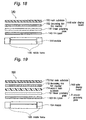
As shown in Fig. 18, in a watch structure 140 according
to the present embodiment, a solar cell 142 and a module 144
are fixed through a middle frame 146 to an outer case which is
not shown in the same manner as that in the thirteenth embodiment.
-
A circular polarizing plate A constituted by a linear
polarizing plate 141 and a 1/4λ plate 143 is provided above
the middle frame 146. Furthermore, a solar display board 148
is provided thereabove.
-
The solar display board 148 according to the present
embodiment includes a resin substrate 150 having a pattern and
a decorating thin film member 152.
-
Since the material and fabricating method for the resin
substrate 150 having a pattern are same as those in the thirteenth
embodiment, detailed description thereof will be omitted.
-
The decorating thin film member 152 is not particularly
restricted but may be any of various thin layer articles having
a pattern, coloring or the like. Examples of the decorating
thin film member 152 include a thin layer article formed of a
natural material such as a cloth, a paper, a thinly sliced shell
or a wood, a ceramic sheet, a polarizing film, a coloring film,
an electroforming foil, an electrodeposited image, an etched
metal foil (etched image), a film on which a hologram is printed
out (a hologram image) and the like. The thickness of the
decorating thin film member 152 is preferably approximately 5
to 300 µm, and more preferably approximately 10 to 200 µm.
-
The resin substrate 150 is bonded to the decorating thin
film member 152 through, for example, adhesion using an adhesive,
bonding using a glue, film bonding, melting bonding, high
frequency bonding or the like.
-
In this case, the whole thickness of the display board
148 including the resin substrate 150 and the decorating thin
film member 152 is not particularly restricted but is preferably
60 to 800 µm, and more preferably 300 to 500 µm.
-
The display board according to the present invention,
moreover, it is desirable that a light transmittance (a visible
light range or wavelength : 600 nm) should be 10 % or more,
preferably 20 % or more, and more preferably 30 % or more by
proper selection of the material and the thickness. A display
board having such a light transmittance can be preferably used
as a clock dial of a solar charging driving type which has recently
spread in the market. This is the same as in the following
embodiments.
-
With such a structure, a boundary line between the solar
cell 142 and the middle frame 146, a gate track generated through
injection molding of the middle frame 146, and furthermore, a
solar cell element dividing line of the solar cell 142 cannot
be seen still more than those in the fourth embodiment. As a
result, a variation in the design of the solar display board
148 can further be increased.
-
Furthermore, a decoration which is present on the upper
surface of the solar display board 148 such as a cloth, a paper,
a rift, a grain, a pyroxene, a leaf, a petal, a shell, a leather
and various transferred fine patterns to be the pattern portion
152 of the resin substrate 150 and a decoration which is present
thereunder, for example, a thin layer article formed of a natural
material such as a cloth, a paper, a shell or a wood of the
decorating thin film member 152, a polarizing film, a coloring
film, an electroforming foil or an electrodeposited image
produce a decorative property. Therefore, the design having
a three-dimensional effect and a feeling of high quality can
be implemented.
-
Consequently, the feeling of high quality of the solar
display board 148 can be produced. In addition, it is possible
to increase a variation in design in which a decorative property
is great and the depth of a pattern and a three-dimensional effect
are excellent. Thus, the feeling of high quality can be produced
as goods. Moreover, the middle frame is provided. Therefore,
various external shapes of the watch can be obtained in respect
of the design.
(Fifteenth Embodiment)
-
As shown in Fig. 19, in a watch structure 160 according
to the present embodiment, a solar cell 162 and a module 164
are fixed through a middle frame 166 to an outer case which is
not shown in the same manner as that in the thirteenth embodiment.
-
A circular polarizing plate A constituted by a linear
polarizing plate 161 and a 1/4λ plate 163 is provided above
the middle frame 166. Furthermore, a solar display board 168
is provided thereabove.
-
The solar display board 168 according to the present
embodiment has a first resin substrate 170, a decorating thin
film member 172 and a second resin substrate 174 provided in
this order.
-
The first resin substrate 170 and the second resin
substrate 174 are formed of the same material as that of the
resin substrate 110 of the display board 108 according to the
thirteenth embodiment.
-
In the solar display board 168 according to the present
embodiment, it is not necessary to form a pattern on the first
resin substrate 170 and the second resin substrate 174. However,
the pattern may be formed on either or both of them in the same
manner as the resin substrate 110 of the display board 108
according to the thirteenth embodiment. In this case, the same
method as that described in the thirteenth embodiment can be
employed for forming the pattern, and preferably, a pattern
transfer method using a thermal press by means of a pattern mold
can be employed.
-
Moreover, the decorating thin film member 172 is the same
as the decorating thin film member 152 according to the fourteenth
embodiment.
-
Furthermore, it is desirable that the decorating thin film
member 172 should be provided between the first resin substrate
170 and the second resin substrate 174 through one of adhesion
using an adhesive, bonding using a glue, film bonding, bonding
using an adhesive, melting bonding and high frequency bonding
in consideration of a mechanical strength, a removing property
and a transmittance.
-
A thickness of the first resin substrate 170 in the solar
display board 168 is preferably 50 to 500µm, and more preferably
80 to 200µm. A thickness of the decorating thin film member
172 is preferably 5 to 300µm, and more preferably 10 to 200
µm. A thickness of the second resin substrate 174 is preferably
50 to 500µm, and more preferably 80 to 200µm.
-
A whole thickness of the solar display board 168 including
the resin substrates 170 and 174 and the decorating thin film
member 172 is not particularly restricted but is preferably 110
to 1300µm, and more preferably 300 to 500µm.
-
With such a structure, a boundary line between the solar
cell 162 and the middle frame 166, a gate track generated through
injection molding of the middle frame 166, and furthermore, a
solar cell element dividing line of the solar cell 162 cannot
be seen still more than those in the fourth embodiment. As a
result, a variation in the design of the solar display board
168 can further be increased.
-
Furthermore, a decoration which is present on the upper
or lower surface of the solar display board 168 such as a cloth,
a paper, a rift, a grain, a pyroxene, a leaf, a petal, a shell,
a leather and various transferred fine patterns to be the pattern
portion of the first resin substrate 170 or the second resin
substrate 174 and a decoration which is present in the middle
thereof, for example, a thin layer article formed of a natural
material such as a cloth, a paper, a shell or a wood of the
decorating thin film member 172, a polarizing film, a coloring
film, an electroforming foil or an electrodeposited image produce
a decorative property. As a result, the design having a
three-dimensional effect and a feeling of high quality can be
attained.
-
Consequently, the feeling of high quality of the solar
display board 168 can be produced. In addition, it is possible
to increase a variation in design in which the depth of a pattern
and a three-dimensional effect are excellent. Thus, the feeling
of high quality can be produced as goods. Moreover, the middle
frame is provided. Therefore, various external shapes of the
watch can be obtained in respect of the design.
(Sixteenth Embodiment)
-
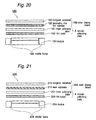
As shown in Fig. 20, in a watch structure 180 according
to the present embodiment, a solar cell 182 and a module 184
are fixed through a middle frame 186 to an outer case which is
not shown in the same manner as that in the thirteenth embodiment.
-
A circular polarizing plate A constituted by a linear
polarizing plate 181 and a 1/4λ plate 183 is provided above
the middle frame 186. Furthermore, a solar display board 188
is provided thereabove.
-
The solar display board 188 according to the present
embodiment has an inorganic substrate 190 having a pattern and
a decorating thin film member 192 fixed to the inorganic
substrate.
-
The inorganic substrate 190 is formed of a glass, a sapphire
glass or a ceramic plate, and preferably the glass or the sapphire
glass. The inorganic substrate 190 may be transparent or may
be colored and translucent. A pattern is formed on the inorganic
substrate 190 through machining such as engraving or rubbing,
etching using hydrofluoric acid, the electric forming method
and the pattern transfer method using a thermal press described
in the thirteenth embodiment or the like. Moreover, the
decorating thin film member 192 maybe the same as the decorating
thin film member 192 according to the fourteenth embodiment.
-
A thickness of the inorganic substrate 190 in the solar
display board 188 is preferably 50 to 500µm, and more preferably
200 to 300µm. A thickness of the decorating thin film member
192 is preferably 5 to 300µm, and more preferably 10 to 200
µm.
-
A whole thickness of the solar display board 188 including
the inorganic substrates 190 and the decorating thin film member
192 is not particularly restricted but is preferably 60 to 800
µm, and more preferably 300 to 600µm.
-
In this case, it is desirable that the inorganic substrate
190 and the decorating thin film member 192 should be fixed by
one of adhesion using an adhesive, bonding using a glue, film
bonding, bonding using an adhesive, melting bonding and high
frequency bonding in consideration of a mechanical strength,
a removing property and a transmittance.
-
With such a structure, a boundary line between the solar
cell 182 and the middle frame 186, a gate track generated through
injection molding of the middle frame 186, and furthermore, a
solar cell element dividing line of the solar cell 182 cannot
be seen still more than those in the fourth embodiment. As a
result, a variation in the design of the solar display board
188 can further be increased.
-
Furthermore, the pattern portion of the inorganic
substrate 190 present on the upper surface of the solar display
board 188 and a decoration which is present thereunder, for
example, a thin layer article formed of a natural material such
as a cloth, a paper, a shell or a wood of the decorating thin
film member 192, a polarizing film, a coloring film, an
electroforming foil or an electrodeposited image produce a
decorative property. Therefore, the design having a
three-dimensional effect and a feeling of high quality can be
implemented.
-
Consequently, the feeling of high quality of the solar
display board 188 can be produced. In addition, it is possible
to increase a variation in design in which a decorative property
is great and the depth of a pattern and a three-dimensional effect
are excellent. Thus, the feeling of high quality can be produced
as goods. Moreover, the middle frame is provided. Therefore,
various external shapes of the watch can be obtained in respect
of the design.
(Seventeenth Embodiment)
-
As shown in Fig. 21, in a watch structure 200 according
to the present embodiment, a solar cell 202 and a module 204
are fixed through a middle frame 206 to an outer case which is
not shown in the same manner as that in the thirteenth embodiment.
-
A circular polarizing plate A constituted by a linear
polarizing plate 201 and a 1/4λ plate 203 is provided above
the middle frame 206. Furthermore, a solar display board 208
is provided thereabove.
-
The solar display board 208 according to the present
embodiment is constituted by stacking an inorganic substrate
210 and a resin substrate 212.
-
In this case, the materials of the inorganic substrate
210 and the resin substrate 212 are the same as those of the
inorganic substrate 190 according to the sixteenth embodiment
and the resin substrate 110 according to the thirteenth
embodiment, respectively. In the solar display board 208, a
pattern does not need to be formed on the inorganic substrate
210 and the resin substrate 212 and a pattern may be formed on
either or both of them. In particular, it is preferable that
the pattern should be formed on the resin substrate 212 by using
a pattern transfer method.
-
A thickness of the inorganic substrate 210 in the solar
display board 208 is preferably 50 to 500µm, and more preferably
200 to 300µm. A thickness of the resin substrate 212 is
preferably 50 to 500µm, and more preferably 100 to 200µm.
-
A whole thickness of the solar display board 208 including
the inorganic substrate 210 and the resin substrate 212 is not
particularly restricted but is preferably 100 to 1000µm, and
more preferably 300 to 600µm.
-
It is desirable that the resin substrate 212 and the
inorganic substrate 210 should be fixed through one of adhesion
using an adhesive, bonding using a glue, film bonding, bonding
using an adhesive, melting bonding and high frequency bonding
in consideration of a mechanical strength, a removing property
and a transmittance.
-
With such a structure, a boundary line between the solar
cell 202 and the middle frame 206, a gate track generated through
injection molding of the middle frame 206, and furthermore, a
solar cell element dividing line of the solar cell 202 cannot
be seen still more than those in the fourth embodiment. As a
result, a variation in the design of the solar display board
208 can further be increased.
-
Furthermore, the pattern portion of the inorganic
substrate 210 present on the upper surface of the solar display
board 208 and a decoration which is present thereunder and is
the pattern portion of the resin substrate 212 such as a cloth,
a paper, a rift, a grain, a pyroxene, a leaf, a petal, a shell,
a leather and various transferred fine patterns produce a
decorative property. As a result, the design having a
three-dimensional effect and a feeling of high quality can be
implemented.
-
Consequently, the feeling of high quality of the solar
display board 208 can be produced. In addition, it is possible
to increase a variation in design in which a decorative property
is great and the depth of a pattern and a three-dimensional effect
are excellent. Thus, the feeling of high quality can be produced
as goods. Moreover, the middle frame is provided. Therefore,
various external shapes of the watch can be obtained in respect
of the design.
(Eighteenth Embodiment)
-
As shown in Fig. 22, in a watch structure 220 according
to the present embodiment, a solar cell 222 and a module 224
are fixed through a middle frame 226 to an outer case which is
not shown in the same manner as that in the thirteenth embodiment.
-
A circular polarizing plate A constituted by a linear
polarizing plate 221 and a 1/4λ plate 223 is provided above
the middle frame 226. Furthermore, a solar display board 228
is provided thereabove.
-
The solar display board 228 according to the present
embodiment is formed of only the inorganic substrate 230.
-
In this case, it is desirable that the material of the
inorganic substrate 230 shouldbe the same as that of the inorganic
substrate 190 according to the sixteenth embodiment and should
be colored with a pigment or a dye.
-
In the solar display board 228, moreover, a pattern does
not need to be formed on the inorganic substrate 203 but is
preferably formed.
-
A whole thickness of the solar display board 228 is not
particularly restricted but is preferably 100 to 1000µm, and
more preferably 300 to 600µm.
-
With such a structure, a boundary line between the solar
cell 222 and the middle frame 226, a gate track generated through
injection molding of the middle frame 226, and furthermore, a
solar cell element dividing line of the solar cell 222 cannot
be seen still more than those in the fourth embodiment. As a
result, a variation in the design of the solar display board
228 can further be increased.
-
Furthermore, a decoration of the pattern portion of the
inorganic substrate 230 present on the upper surface of the solar
display board 228 produces a decorative property so that the
design having a three-dimensional effect and a feeling of high
quality can be implemented.
-
Consequently, the feeling of high quality of the solar
display board 228 can be produced. In addition, it is possible
to increase a variation in design in which a decorative property
is great and the depth of a pattern and a three-dimensional effect
are excellent. Thus, the feeling of high quality can be produced
as goods. Moreover, the middle frame is provided. Therefore,
various external shapes of the watch can be obtained in respect
of the design.
(Nineteenth Embodiment)
-
As shown in Fig. 23, in a watch structure 240 according
to the present embodiment, a solar cell 242 and a module 244
are fixed through a middle frame 246 to an outer case which is
not shown in the same manner as that in the thirteenth embodiment.
-
A circular polarizing plate A constituted by a linear
polarizing plate 241 and a 1/4λ plate 243 is provided above
the middle frame 246. Furthermore, a solar display board 248
is provided thereabove.
-
The solar display board 248 according to the present
embodiment is formed by stacking a first inorganic substrate
250, a decorating thin film member 252 and a second inorganic
substrate 254.
-
The first inorganic substrate 250 and the second inorganic
substrate 254 can be the same as the inorganic substrate 190
according to the sixteenth embodiment.
-
In the solar display board 248, a pattern does not need
to be formed on the first inorganic substrate 250 and the second
inorganic substrate 254 but is desirably formed on either or
both of them. Moreover, the decorating thin film member 252
can be the same as the decorating thin film member 152 according
to the fourteenth embodiment.
-
A thickness of the first inorganic substrate 250 in the
solar display board 248 is preferably 50 to 500µm, and more
preferably 200 to 300µm. A thickness of the decorating thin
film member 252 is preferably 5 to 300µm, and more preferably
10 to 200µm. A thickness of the second inorganic substrate
254 is preferably 50 to 500µm, and more preferably 200 to 300
µm.
-
A whole thickness of the solar display board 248 including
the inorganic substrates 250 and 254 and the decorating thin
film member 252 is not particularly restricted but is preferably
110 to 1300µm, and more preferably 300 to 600µm.
-
It is desirable that the decorating thin film member 252
should be fixed between the first inorganic substrate 250 and
the second inorganic substrate 254 through one of adhesion using
an adhesive, film bonding, bonding using an adhesive, melting
bonding and high frequency bonding in consideration of a
mechanical strength, a removing property and a transmittance.
-
With such a structure, a boundary line between the solar
cell 242 and the middle frame 246, a gate track generated through
injection molding of the middle frame 246, and furthermore, a
solar cell element dividing line of the solar cell 242 cannot
be seen still more than those in the fourth embodiment. As a
result, a variation in the design of the solar display board
248 can further be increased.
-
Furthermore, a decoration of the pattern portions of the
inorganic substrates 250 and 254 which are present on the upper
and lower surfaces of the solar display board 248 and a decoration
which is present in the middle thereof, for example, a thin layer
article formed of a natural material such as a cloth, a paper,
a shell or a wood, a polarizing film, a coloring film, an
electroforming foil or an electrodeposited image in the
decorating thin film member 252 produce a decorative property.
As a result, the design having a three-dimensional effect and
a feeling of high quality can be implemented.
-
Consequently, the feeling of high quality of the solar
display board 248 can be produced. In addition, it is possible
to increase a variation in design in which a decorative property
is great and the depth of a pattern and a three-dimensional effect
are excellent. Thus, the feeling of high quality can be produced
as goods. Moreover, the middle frame is provided. Therefore,
various external shapes of the watch can be obtained in respect
of the design.
(Twentieth Embodiment)
-
As shown in Fig. 24, in a watch structure 260 according
to the present embodiment, a solar cell 262 and a module 264
are fixed through a middle frame 266 to an outer case which is
not shown in the same manner as that in the thirteenth embodiment.
-
A circular polarizing plate A constituted by a linear
polarizing plate 261 and a 1/4λ plate 263 is provided above
the middle frame 266. Furthermore, a solar display board 268
is provided thereabove.
-
The solar display board 268 according to the present
embodiment is constituted by stacking a resin substrate 270,
a decorating thin film member 272 and an inorganic substrate
274 in this order.
-
In this case, the resin substrate 270, the decorating thin
film member 272 and the inorganic substrate 274 can be the same
as the resin substrate 110 according to the thirteenth embodiment,
the decorating thin film member 152 according to the fourteenth
embodiment and the inorganic substrate 190 according to the
sixteenth embodiment, respectively.
-
Moreover, a pattern does not need to be formed on the resin
substrate 270 and the inorganic substrate 274 but is desirably
formed on either or both of them.
-
In this case, one or more resin substrates, decorating
thin film members and inorganic substrates may be used and may
have three or more layers, respectively. Moreover, the order
of the stack of the resin substrate, the decorating thin film
member and the inorganic substrate is not particularly restricted.
Furthermore, two or more kinds of resin substrates may be used.
Similarly, two or more kinds of decorating thin film members
and inorganic substrates may be used, respectively.
-
Such a
solar display board 268 has the following preferable
layer structures including the structure shown in Fig. 24,
- (1) resin substrate / decorating thin film member / resin
substrate / inorganic substrate,
- (2) resin substrate / decorating thin film member / inorganic
substrate / resin substrate,
- (3) decorating thin film member / inorganic substrate / resin
substrate, and
- (4) inorganic substrate / decorating thin film member /
inorganic substrate / resin substrate.
-
-
In this case, a thickness of the resin substrate is
preferably 50 to 500 µm and more preferably 80 to 200 µm per
layer. A thickness of the decorating thin film member is
preferably 5 to 300 µm and more preferably 10 to 200 µm per
layer. A thickness of the inorganic substrate is preferably
50 to 500 µm and more preferably 200 to 300 µm per layer.
-
A whole thickness of the solar display board 268 including
the resin substrate, the decorating thin film member and the
inorganic substrate is not particularly restricted but is
preferably 110 to 1300µm, and more preferably 300 to 600µ
m.
-
With such a structure, a boundary line between the solar
cell 262 and the middle frame 266, a gate track generated through
injection molding of the middle frame 266, and furthermore, a
solar cell element dividing line of the solar cell 262 cannot
be seen still more than those in the fourth embodiment. Therefore,
a variation in the design of the solar display board 268 can
further be increased.
-
Furthermore, a decoration such as a cloth, a paper, a rift,
a grain, a pyroxene, a leaf, a petal, a shell, a leather and
various transferred fine patterns to be the pattern portion of
the resin substrate 270, a decoration of the pattern portion
of the inorganic substrate 274 and a decoration of the decorating
thin film member 272 such as a thin layer article formed of a
natural material, for example, a cloth, a paper, a shell or a
wood, a polarizing film, a coloring film, an electroforming foil
or an electrodeposited image produce a decorative property. As
a result, the design having a three-dimensional effect and a
feeling of high quality can be implemented.
-
Consequently, the feeling of high quality of the solar
display board 248 can be produced. In addition, it is possible
to increase a variation in design in which a decorative property
is great and the depth of a pattern and a three-dimensional effect
are excellent. Thus, the feeling of high quality can be produced
as goods. Moreover, the middle frame is provided. Therefore,
various external shapes of the watch can be obtained in respect
of the design.
(Twenty-first Embodiment)
-
As shown in Fig. 25, in a watch structure 280 according
to the present embodiment, a solar cell 282 and a module 284
are fixed through a middle frame 286 to an outer case which is
not shown in the same manner as that in the thirteenth embodiment.
-
A circular polarizing plate A constituted by a linear
polarizing plate 281 and a 1/4λ plate 283 is provided above
the middle frame 286. Furthermore, a solar display board 288
is provided thereabove.
-
The solar display board 288 according to the present
embodiment is constituted by a metal plate 290.
-
The metal plate 290 has a window portion 292 of a display
section formed in a central part thereof through machining such
as punching, and a pattern 294 is formed on a surface thereof.
-
While the metal plate 290 is not particularly restricted
but a metal, for example, phosphor bronze, titanium, stainless
steel such as SUS 304, a copper alloy such as brass, nickel silver
or the like can be used.
-
As a method of forming a pattern on the surface of the
metal plate 290, a pattern forming method of forming a pattern
through a press using a pattern mold and a machining method using
engraving, rubbing or the like can be used.
-
For the metal plate 290, it is also possible to use a metal
thin film having a pattern shape which is obtained by forming
a pattern on a metal substrate through a photoresist, plating
the pattern with a metal, forming a pattern metal thin layer,
coating an adhesive on the surface of the metal thin film layer
and removing the metal substrate.
-
It is desirable that the metal plate 290 should be fixed
to the upper surface of the circular polarizing plate A through
bonding using a glue, film bonding, bonding using an adhesive
or the like in consideration of a mechanical strength, a removing
property and a transmittance.
-
With such a structure, a boundary line between the solar
cell 282 and the middle frame 286, a gate track generated through
injection molding of the middle frame 286, and furthermore, a
solar cell element dividing line of the solar cell 282 cannot
be seen still more than those in the fourth embodiment so that
a variation in the design of the solar display board 288 can
further be increased.
-
Furthermore, the decorative property of the metal plate
290 which is present on the upper surface of the solar display
board 288 can implement the design having a three-dimensional
effect and a feeling of high quality.
-
Consequently, the feeling of high quality of the solar
display board 288 can be produced. In addition, it is possible
to increase a variation in design in which a decorative property
is great and the depth of a pattern and a three-dimensional effect
are excellent. Thus, the feeling of high quality can be produced
as goods. Moreover, the middle frame is provided. Therefore,
various external shapes of the watch can be obtained in respect
of the design.
-
An auxiliary member formed of a transparent resin such
as polycarbonate can also be provided between the solar display
board according to each of the thirteenth to twenty-first
embodiments and the circular polarizing plate A to adjust a
portion between the circular polarizing plate A and the solar
display board to the thickness of an outer case, which is not
shown.
-
On the surface of the solar display board according to
the embodiment of the present invention, moreover, a display
portion (a time scale of a watch) , the name of a manufacturer,
a type and the like can be displayed by means of printing or
a decorating member (a time letter, a mark or the like) to be
fabricated by electroforming and fixed with an adhesive can be
provided.
-
Furthermore, while the description has been given to only
the watch in the above-mentioned embodiments, the present
invention is not restricted thereto but the same effects can
be obtained, that is, a variation in design can be increased
through utilization for other electronic apparatuses having a
solar cell, for example, an electronic calculator, a radio, a
battery charger or the like. Thus, various changes can be made
without departing from the scope of the present invention.
Effects of the Invention
-
According to the present invention, the circular
polarizing plate constituted by the linear polarizing plate and
at least one phase difference plate is provided between the middle
frame for fixing the module having the solar cell to the case
and the solar display board. Consequently, a boundary line
between the solar cell and the middle frame, agate track generated
through injection molding of the middle frame, and furthermore,
a solar cell element dividing line of the solar cell cannot be
seen. As a result, a variation in design of the solar display
board can be increased. Moreover, the color of the solar display
board is deepened so that a feeling of high quality can be obtained
as goods.
-
According to the present invention, furthermore, the
surface of the circular polarizing plate is provided with a solar
display board constituted by a resin substrate having a pattern,
an inorganic substrate having a pattern or a decorating thin
film member or a combination thereof. Therefore, a decorative
property is great, the pattern becomes rich and an excellent
three-dimensional effect can be obtained. Through a
combination of two or more patterns or two or more materials,
moreover, it is possible to manufacture a display board having
a better feeling of beauty than ever. Thus, a design variation
can be increased.