JP4098952B2 - Timepiece dial and method for manufacturing the same - Google Patents
Timepiece dial and method for manufacturing the same Download PDFInfo
- Publication number
- JP4098952B2 JP4098952B2 JP2000335074A JP2000335074A JP4098952B2 JP 4098952 B2 JP4098952 B2 JP 4098952B2 JP 2000335074 A JP2000335074 A JP 2000335074A JP 2000335074 A JP2000335074 A JP 2000335074A JP 4098952 B2 JP4098952 B2 JP 4098952B2
- Authority
- JP
- Japan
- Prior art keywords
- convex portion
- pattern
- film
- substrate
- transparent
- Prior art date
- Legal status (The legal status is an assumption and is not a legal conclusion. Google has not performed a legal analysis and makes no representation as to the accuracy of the status listed.)
- Expired - Fee Related
Links
Images


Description
【0001】
【発明の属する技術分野】
本発明はソーラセル用の時計用文字板及びその製造方法に関する。
【0002】
【従来の技術】
ソーラセル用の時計用文字板に、金属感を出現させると共にソーラセルの濃紫色が見えないようにする技術の一つとして従来図10に示す構成のものがある。図10は時計用文字板の要部拡大断面図を示すもので、この時計用文字板は透明なプラスチック板などからなる透過性基板1の下面に小孔2aが均等間隔に多数設けられた金属膜2を形成した構成となっている。そして、この小孔2aは30μmより小さく形成されている。小孔の大きさが30μmより小さいとその小孔自体が目に殆ど見えず、従って、その下に配設されるソーラセル自体も全く見えない。
【0003】
時計用のソーラセルは一般的に、図11に示すように4等分割された4面(A1、A2、A3、A4)に設けられて、文字板の下面側に配設される。そして、文字板からの透過光量は4面に等しく放射されるように設計される。小孔2aを均等間隔に設けることによって4等分割されたソーラセルのそれぞれに等しく透過光が放射される。更に、均等間隔に多数設けられる小孔2aは、その小孔2aの総面積が文字板面積の25〜50%の範囲内で設けられる。小孔2aの総面積が25%あれば透過率が25%確保でき、十分な発電量を得ることができる。また、この小孔2aの総面積が50%を越えるとソーラセルの濃紫色が強く見えてくるようになる。
【0004】
上記構成の時計用文字板は図12に示す工程によって形成される。図12は製造方法を示す工程説明図である。図12(a)は透明なプラスチック板などからなる透過性基板1に金属膜2を形成した状態を示す図で、金属膜2は蒸着方法によって形成する。この金属膜2はアルミ、ニッケルなどの各種の金属が選択でき、その厚みは光が透過しない程度の厚みに形成される。
【0005】
次に、図12(b)は図12(a)で形成した金属膜2の上面にレジスト膜3を形成した状態を示す図で、レジスト膜3は印刷や塗装などの公知の方法で形成される。
【0006】
次に、図12(c)は露光工程を示し、レジスト膜3の上面側にネガパターンフィルム4を載置して紫外線を照射し、露光している状態を示す図である。このネガパターンフィルム4は、小孔2aが均等間隔に多数設けた金属膜2に等しく対応させた被印刷体形状のネガパターンフィルムで、このネガパターンフィルム4の上から紫外線を照射してレジスト膜3を露光硬化させる。これによって、レジスト膜3の小孔2aに対応する部分は紫外線が照射されないので柔らかい状態にあり、それ以外の部分(図中矢印で示す)は紫外線が照射されて硬化状態になる。
【0007】
次に、図12(d)はレジスト膜3に小孔3aを形成した状態を示す図である。図12(c)で露光されなかったレジスト膜3の柔らかい部分(ちょうど小孔2aに対応する部分にあたる)を剥離液でもって剥離すると、小孔3aを形成したレジスト膜3が得られる。このレジスト膜3の小孔3a部分は金属膜2の小孔2a部分に対応する。
【0008】
次に、図12(e)はレジスト膜3の小孔3a部分に露出する金属膜2をエッチング液によって剥離し、小孔2aを形成した状態を示す図である。エッチング液で露出している金属膜2を剥離することによって小孔2aが形成される。
【0009】
次に、図12(f)は残っているレジスト膜3を全部剥離して金属膜2を露出させた状態を示す図である。剥離液でレジスト膜3を全部剥離することによって小孔2aを形成した金属膜2が現れる。このようにして文字板の金属膜2を形成し、この金属膜2の面を下面側にして使用すれば図10に示す構成の文字板が得られる。
【0010】
【発明が解決しようとする課題】
このような方法で形成したソーラセル用の時計用文字板は、金属感が現れて、しかもソーラセルの濃紫色が全く見えないものになる。しかしながら、製作工程が多いためコスト的に非常に高いものになっていた。また、小孔が非常に小さいため、寸法精度や位置精度もレジスト膜の厚みやフィルムの伸縮、及び金属膜のサイドエッチングなどの影響を受け、非常に精度良く仕上げることが難しいものとなっていた。従って、歩留まりも低いものとなり量産性には向いていなかった。また、エッチング液や剥離液を使用することから身体的に好ましい作業とは言えないものであった。
【0011】
【課題を解決するための手段】
本発明は上記課題に鑑みて成されたもので、その目的とするところは簡単な作業であって安いコストで製作でき、しかも精度良く作ることができて、且つ身体に害のない安全な作業で製作することができるソーラセル用時計用文字板及びその製造方法を提供することである。
【0012】
そして課題を解決するための手段として、時計用文字板においては、請求項1に係る発明は、ソーラセルと、該ソーラセルの上側に配置された透過性基板であって、該透過性基板の下面に模様状に形成された凹凸部を有し、前記凹部には非透過膜を有し、前記凸部の上面は平滑面になっていて透過性を有し、前記凸部の高さが少なくとも10μm以上であって、凸部の上面は、その総面積が前記透過性基板の面積に対して20〜50%を有し、更に、この平滑な上面の幅は70μmより細いことを特徴とする。
【0013】
また、請求項2に係る発明は、ソーラセルと、該ソーラセルの上側に配置された透過性基板であって、該透過性基板の下面に模様状に形成された凹凸部を有し、前記凹部には透過性カラー装飾膜と非透過膜とを積層して有し、前記凸部の上面は平滑面になっていて透過性を有し、前記凸部の高さが少なくとも10μm以上であって、凸部の上面は、その総面積が前記透過性基板の面積に対して20〜50%を有し、更に、この平滑な上面の幅は70μmより細いことを特徴とする。
【0014】
また、請求項3に係る発明は、前記模様状に形成された凹凸部は一定な間隔で並んで形成されていることを特徴とする。
【0015】
また、請求項4に係る発明は、前記凹凸部の模様はストライプ模様、格子模様、サークル模様、幾何学模様などであることを特徴とする。
【0016】
また、請求項5に係る発明は、前記非透過膜は金属膜又は塗料膜であることを特徴とする。
【0017】
また、請求項6に係る発明は、前記透過性カラー装飾膜は金属薄膜又は塗料膜であることを特徴とする。
【0018】
また、請求項7に係る発明は、ソーラセルと、該ソーラセルの上側に配置された透過性基板であって、該透過性基板の下面に模様状に形成された凹凸部を有し、前記凹部には非透過膜を有し、前記凸部の上面は平滑面になっていて透過性を有し、前記凸部の高さが少なくとも10μm以上であって、凸部の上面は、その総面積が前記透過性基板の面積に対して20〜50%を有し、この平滑な上面の幅は100μmより細く、更に、前記透過性基板の上面に凹凸部を有する第2の模様が形成されていることを特徴とする。また、請求項8に係る発明は、ソーラセルと、該ソーラセルの上側に配置された透過性基板であって、該透過性基板の下面に模様状に形成された凹凸部を有し、前記凹部には透過性カラー装飾膜と非透過膜とを積層して有し、前記凸部の上面は平滑面になっていて透過性を有し、前記凸部の高さが少なくとも10μm以上であって、凸部の上面は、その総面積が前記透過性基板の面積に対して20〜50%を有し、更に、この平滑な上面の幅は100μmより細く、更に、前記透過性基板の上面に凹凸部を有する第2の模様が形成されていることを特徴とする
【0019】
次に、時計用文字板の製造方法においては、請求項9に係る発明は、金型を使用してプラスチック射出成形方法又は透過性のプラスチック板を加熱・加圧した方法によって、下面に一定の間隔で並んだ模様状の凹凸部を有し、且つ、該凸部上面の幅が70μmより細い透過性基板を形成する工程と、前記透過性基板の凹凸部に蒸着方法又は塗装方法によって非透過膜を形成する工程と、切削方法又は研磨方法によって前記透過性基板の凸部の非透過膜を除去すると共に、前記凸部の上面を平滑面に形成し、前記凸部の高さが少なくとも10μm以上であって、且つ、該凸部上面の総面積が前記透過性基板の面積に対して20〜50%にする工程と、を有することを特徴とする。
【0020】
また、請求項10に係る発明は、金型を使用してプラスチック射出成形方法又は透過性のプラスチック板を加熱・加圧した方法によって、下面に一定の間隔で並んだ模様状の凹凸部を有し、且つ、該凸部上面の幅が70μmより細い透過性基板を形成する工程と、前記透過性基板の凹凸部に蒸着方法又は塗装方法によって透過性カラー装飾膜を形成する工程と、金属感と装飾感を高めるため前記形成した透過性カラー装飾膜の上に蒸着方法又は塗装方法によって非透過膜を形成する工程と、切削方法又は研磨方法によって前記透過性基板の凸部の非透過膜と透過性カラー装飾膜とを除去すると共に、前記凸部の上面を平滑面に形成し、前記凸部の高さが少なくとも10μm以上であって、且つ、前記凸部上面の総面積が前記透過性基板の面積に対して20〜50%にする工程と、を有することを特徴とする。
【0025】
また、請求項11に係る発明は、前記模様状の凹凸部は一定な間隔で並んで形成され、前記凹凸部の模様はストライプ模様、格子模様、サークル模様、幾何学模様などであることを特徴とする。
【0026】
また、請求項12に係る発明は、前記非透過膜は金属膜又は塗料膜であることを特徴とすることを特徴とする。
【0027】
また、請求項13に係る発明は、前記透過性カラー装飾膜は金属薄膜又は塗料膜であることを特徴とする。
【0028】
また、請求項14に係る発明は、金型を使用してプラスチック射出成形方法又は透過性のプラスチック板を加熱・加圧した方法によって、上面に凹凸部を有する第2の模様を形成し、下面に一定の間隔で並んだ模様状の凹凸部を有し、且つ、該凸部上面の幅が100μmより細い透過性基板を形成する工程と、前記透過性基板の下面の凹凸部に蒸着方法又は塗装方法によって非透過膜を形成する工程と、切削方法又は研磨方法によって前記透過性基板の凸部の非透過膜を除去すると共に、前記凸部の上面を平滑面に形成し、前記下面の凸部の高さが少なくとも10μm以上に形成し、且つ、該凸部上面の総面積が前記透過性基板の面積に対して20〜50%にする工程と、を有することを特徴とする。また、請求項15に係る発明は、金型を使用してプラスチック射出成形方法又は透過性のプラスチック板を加熱・加圧した方法によって、上面に凹凸部を有する第2の模様を形成し、下面に一定の間隔で並んだ模様状の凹凸部を有し、且つ、該凸部上面の幅が100μmより細い透過性基板を形成する工程と、前記透過性基板の下面の凹凸部に蒸着方法又は塗装方法によって透過性カラー装飾膜を形成する工程と、金属感と装飾感を高めるため前記形成した透過性カラー装飾膜の上に蒸着方法又は塗装方法によって非透過膜を形成する工程と、切削方法又は研磨方法によって前記透過性基板の凸部の非透過膜と透過性カラー装飾膜とを除去すると共に、前記凸部の上面を平滑面に形成し、前記下面の凸部の高さが少なくとも10μm以上に形成し、且つ、前記凸部上面の総面積が前記透過性基板の面積に対して20〜50%にする工程と、を有することを特徴とする。
【0029】
【発明の実施の形態】
以下、図面に基づいて本発明の実施形態を説明する。先ず本発明の第1の実施形態に係わる時計用文字板とその製造方法を図1〜4に基づいて説明する。図1は時計用文字板の要部拡大断面図、図2は図1に示す時計用文字板をその下面側から見た要部拡大斜視図である。また、図3は図1に示す時計用文字板の一製造方法を示す工程説明図、図4は他の製造方法を示す工程説明図である。
【0030】
図1において、文字板10はその下面に凹部11bと凸部11aを形成した透過性基板11と、凹部11bの面に形成した金属の非透過膜12を有している。また、この文字板10は図中省略してあるが、透過性基板11の上面側に時字やマークなどの指標が形成されて完成の仕上がりが成される。
【0031】
上記凸部11aの上面(図中では下表面にあたる)11a1は研磨されて透過性基板11が露出し、更に平滑面になっている。また、この凸部11aはその高さ(h)が少なくても10μm以上あって、上面11a1の幅(t)は70μm以下に形成されている。
【0032】
図2は文字板10の下面側から見た要部斜視図である。凸部11aと凹部11bは一定の間隔で並んで格子状に形成されており、全体的に格子模様を成している。また、図2において、凸部11aの上面11a1は研磨されて平滑面になっている。そして、研磨された上面11a1の総面積は透過性基板11の上面側の面積に対して20〜50%の範囲で形成されているものである。
【0033】
上記金属の非透過膜12は金属を蒸着方法によって形成した金属蒸着膜で、光が透過しない程度の厚みで形成したものである。特に金属に限定するものではなく、印刷や塗装方法で光が透過しない程度の厚みに形成した塗料膜であっても良いものである。
【0034】
上記構成の文字板10においては、凹部11b部分では非透過膜12によって光が透過せず、むしろ反射作用が現れて非透過膜の色調が見える。また、凸部11aの部分では光が透過してその下面に配設したソーラセル(図中略)に入射する。そして、凸部11aの上面11a1は平滑面になっているので散乱することなく入射して入射効率を高める。
【0035】
更に、凸部11aの部分から光が透過するものの、その上面11a1の幅が非常に細いためにソーラセルの濃紫色は殆ど見えない。僅かにカラー着色した透過性基板の下では上面11a1の幅が70μm以下であるとソーラセルの濃紫色は殆ど確認されない。特に、30μm以下になると透明基板であっても全く視認されない。
【0036】
また、凹部11bと凸部11aが下面側に一定の間隔で並んで形成しており、凸部11aの上面11a1の総面積が文字板10の上面側の面積の20〜50%範囲内に形成されているので、ソーラセルの発電に十分な光量を与えることができる。近年のソーラセルには少なくとも20%位の透過率で十分な発電量を得るものが現れてきている。従って、透過部分である上面11a1の総面積が上面側の面積の20%有れば20%の透過率が得られ発電に支障のない光量が得られることになる。また、透過部分である上面11a1の総面積が上面側の面積の50%を越えてくると非透過膜が目立たなくなりソーラセルの濃紫色が目立って見えてくるようになる。このことから、透過部分である上面11a1の総面積を20〜50%の範囲内におさめることによって十分な発電量を得ると共に非透過膜が大きく目について凸部11aの透過部分が全く目立たない。
【0037】
この実施形態は凹凸模様を格子模様に形成したものであるが、ストライプ模様、サークル模様、旭光模様、幾何学模様など各種の模様が同様に選択できるものである。
【0038】
次に、上記構成の文字板10の製造方法を図3及び図4に基づいて説明する。図3は一製造方法の製造工程を示す工程説明図で、いずれも要部断面図で示してある。先ず、図3(a)は射出成形方法で形成した下面に凹部11bと凸部11aを有する透過性基板11のブランク11Aを示している。このブランク11Aは射出成形装置を用いて透過性樹脂を加熱・加圧の基で金型内に射出して成形される。下面の凹凸部は金型に形成した凹凸部から転写によって形成される。
【0039】
次に、図3(b)は凹凸部のある下面全体に金属蒸着膜からなる非透過膜12を形成した図である。射出成形方法によって形成した透過性基板11のプランク11Aの下面全体に蒸着装置で金属蒸着を施して金属蒸着膜の非透過膜12を形成する。この金属蒸着膜は光が透過しない程度の厚み(概ね1000Å以上)に形成する。尚、この非透過膜12は塗装方法で光が透過しない程度の厚みに形成した塗料膜でも良いものである。
【0040】
図3(c)は凸部11aの上面を研磨して非透過膜12を除去し、平滑な上面11a1に仕上げた状態を示す図である。研磨装置によって非透過膜12が形成された凸部11aの上面側を透過性基板が露出する程度まで研磨し、非透過膜12を除去すると共に平滑な上面11a1に仕上げる。尚、本実施の形態においては研磨方法で平滑面に仕上げたが、ダイヤバイトなどを使用して切削方法で平滑面に仕上げても良いものである。
【0041】
以上の製造方法によって文字板10が得られる。上記実施例は片面に凹凸を有する透過性基板を得るのに金型を用いて射出成形方法で形成したものであるが、他の方法として図4に示す方法がある。図4に示すものは、平坦な載品台22上に透過性のプラスチック板21Bを載せ、上から凹凸(23a、23b)の形成された押圧具23でもって加熱の基で加圧すると上記図3(a)で示した透過性基板11のブランク11Aと同じ形状のものが得られる。
【0042】
以上の製造方法をとれば、透過性基板の模様状の凹凸部は、金型または押圧具に形成した模様状の凹凸形状から転写によって形成されるので、寸法及び形状はバラツキの少ない非常に安定した精度で形成することができる。更に、凹凸形状を形成した金型または押圧具は長期間に渡って使用できると共に、この製造加工時間も短時間でできるので量産性に優れ、加工コストも非常に安くすることができる。また、後加工も蒸着加工または塗装加工、研磨加工と簡単な加工方法をとるのでトータルの加工時間も少なくて済み、コスト的にも非常に安くすることができる。更にまた、従来使用した剥離液とかエッチング液などは使用しないので身体への悪影響はなく健康的な作業が可能となる。
【0044】
次に、本発明の第2の実施形態について図5乃至図7に基づいて説明する。図5は本発明の第2の実施形態に係わる時計用文字板の要部拡大断面図、図6は図5に示す時計用文字板を下面側から見た要部断面拡大斜視図である。図7は図5に示す時計用文字板の一製造方法を示す工程説明図である。
【0045】
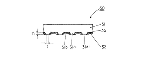
図5において、この文字板30は、その下面側に凹部31bと凸部31aが形成された透過性基板31と、凹部31bに設けられた透過性カラー装飾膜33、このカラー装飾膜33の上に積層された非透過膜32を有している。また、図示してないが、透過性基板31の上面側には時字やマークなどの指標が形成されて完成の仕上がりが成される。
【0046】
ここでの凸部31aは山型状の形状を成しているもので、その上面(図中では下表面)31a1は研磨されて透過性基板31が露出して平滑面になっている。この上面の平滑面はダイヤバイトを用いて切削方法で形成しても良い。また、この凸部31aは、第1の実施形態と同様に、その高(h)さが少なくとも10μm以上あって、上面31a1の幅(t)は70μm以下に形成されている。
【0047】
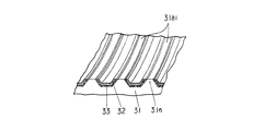
また、この凸部31a及び凹部31bは、図6より、一定の間隔にサークル状に並んでサークル模様を形成している。また、この凸部31aの平滑な上面31a1の総面積は、透過性基板31の上面側の面積に対して20〜50%の範囲で形成されている。
【0048】
上記透過性カラー装飾膜33は、カラー装飾を施すための膜で透過性を持っている。本実施の形態では非常に薄い金属蒸着膜で形成しているが、透過性を有するカラー塗料膜であっても良い。装飾を施したい色調の金属膜や塗料膜を選択する。
【0049】
上記非透過膜32は本実施の形態では白色塗料膜で形成しているが、金属蒸着膜でも良く、光が透過しない程度の厚みに形成する。本実施の形態では透過性カラー装飾膜33に金属蒸着膜、非透過膜32に白色塗料を用いたが、この組み合わせの方がより金属感が現れるからである。また、金属薄膜の透過性カラー装飾膜と塗料の非透過膜との組み合わせ、塗料の透過性カラー装飾膜と金属の非透過膜の組み合わせを行うことにより金属感を出させると共に装飾性を高めることができる。
【0050】
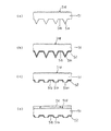
次に、上記文字板30の製造方法を図7に基づいて説明する。図7(a)は金型を用いて射出成形装置で形成したプラスチックの透過性基板31のブランク31Aを示している。このブランク31Aの下面には凹部31bと三角山型の凸部31aが形成されており、いずれも射出成形時に金型から転写して形成する。尚、前述の第1の実施形態で図4に基づいて説明したように、凹凸の設けた加圧具を用い、プラスチック板を加熱の下で加圧して凹凸を形成しても良い。また、凹部31bと凸部31aは、図6で説明したように、サークル状の模様に形成されているものである。
【0051】
図7(b)はブランク31Aの凹凸面上に非常に薄い金属蒸着を施し、透過性カラー装飾膜33を形成した状態を示している。前述したごとく、この透過性カラー装飾膜33は透過性のカラー塗料膜であっても良い。
【0052】
図7(c)は上記図7(b)で形成した透過性カラー装飾膜33の上に白色塗装を施して塗料の非透過膜32を形成した状態を示している。ここでの非透過膜32は光が透過しない程度の厚みに形成する。また、本実施形態では白色塗料を施したが、特に限定するものではなく他の塗料或いは前述したように金属蒸着膜であっても良い。
【0053】
図7(d)は研磨装置で研磨して凸部31aの山を一部削り取ってブランク31Aを露出させ、凸部31aの上面31a1を平滑面に仕上げた状態を示している。この上面31a1の幅は70μm以下の細さに抑えられ、サークル状に現れる凸部31の上面31a1の総面積は透過性基板31の上面の面積に対して20〜50%の範囲内に抑えられている。本実施の形態では研磨方法で凸部31aの山を削り、凸部31aの上面31a1を平滑面に仕上げたが、ダイヤバイトなどを使用して切削方法で平滑面に仕上げることもできる。
【0054】
以上の作業工程を経ることによって図5で示した文字板30を得ることができる。この文字板30は、光を透過する部分の幅が70μm以下と非常に狭い。このため、その下面側に配設されるソーラセルの濃紫色が濃紫色として視認されない。また、幅が30μm以下であると透過部分そのものが見えないため全くソーラセルの色調が見えない。更に、サークル模様状に均一間隔に形成されていると共に光の透過部分の総面積が20〜50%以下の範囲にあるため十分な発電量が得られ、外観的にもカラー装飾膜及び非透過膜の色調などが大きくクローズアップされ、透過部分は殆ど目立たない。
【0055】
また、本実施形態のように凸部を傾斜のもった山型に形成すると、研磨によって光透過部分の大きさを任意に設定することが可能となる。従って、全く視認されない30μm以下の幅も簡単に形成することができる。
【0056】
次に、本発明の第3の実施の形態に係わる時計用文字板及びその製造方法を図8及び図9に基づいて説明する。図8は本発明の第3の実施の形態に係わる時計用文字板の要部拡大断面を示しており、図9はこの時計用文字板の製造方法を説明する工程説明図で、要部拡大断面図を示している。
【0057】
図8より、この文字板50は、その下面に凹部51bと山型形状の凸部51aを有し、その上面に第2の模様51dを有する透過性基板51と、透過性基板51の下面凹部51bに設けた非透過膜52と、透過性基板51の上面の第2の模様51d上に設けた透明保護膜54とを有している。また、図示はしてないが透明保護膜54の上面に時字やマークなどの指標が形成されて完成の仕上がりが成される。
【0058】
上記透過性基板51の下面側に設けられている山型形状の凸部51aの上面51a1は、研磨方法または切削方法によって削られて平滑面になっており、透過性基板51の素地が露出している。そして、凸部51aの高さ(h)は少なくとも10μm以上あって、平滑な上面51a1の幅(t)は大きくても100μm以下に形成されている。
【0059】
透過性基板51の下面側に設けた凹部51bと凸部51aは、図6で示した第2の実施の形態の文字板30と同様、一定の間隔にサークル状に並んでサークル模様状にできている。また、この凸部51aの平滑な上面51a1の総面積は透過性基板51の上面側の面積に対して20〜50%の範囲内で形成されている。
【0060】
凹部51bに形成した非透過膜52は本実施の形態では金属蒸着膜を形成しているが、これは塗料膜であっても良いものである。光が透過しない程度の厚みに形成すれば良い。
【0061】
透過性基板51の上面側に設けた第2の模様51dは本実施の形態では微小の凹凸を成す梨地模様を形成しているが、この第2の模様51dは梨地模様の他に旭光模様,各種の編み目模様、各種の幾何学模様など色々な模様を選択することができる。
【0062】
透過性基板51の第2の模様51d上に設けた透明保護膜54は第2の模様51dを保護するために設けるもので、透明なウレタン樹脂やアクリル樹脂などの塗料を用いて印刷方法や塗装方法などで形成したものである。そして、この透明保護膜54の上面は研磨されて光沢のある平滑面に仕上げられている。
【0063】
本実施の形態においては、透過性基板51の凸部51aの平滑な上面51a1の幅は前述した第1の実施の形態、及び第2の実施の形態の幅より少し大きく形成されて、100μm以下に抑えられている。透過性基板の上面側に凹凸のある第2の模様があると、100μmの幅があってもソーラセルの濃紫色は殆ど見えない。特に、第2の模様が模様目の細かい模様になってくると濃紫色は全く視認されなくなってくる。
【0064】
また、透過性基板51の凸部51aの平滑な上面51a1の総面積が上面側の面積に対して20〜50%の範囲に抑えているので発電に必要な十分な光量を得ることができ、また、非透過膜の色が目立って見えてソーラセルの濃紫色は殆ど見えない。
【0065】
本実施の形態では、透過性基板51の上面に形成した第2の模様が透過性基板51の下面凹部51bに施した非透過膜52の色調のもとで見える文字板が得られる。
【0066】
次に、上記構成を成す文字板50の製造方法を図9に基づいて説明する。図9(a)は射出成形方法で形成した下面に凹部51bと山型状の凸部51aを有し上面に梨地模様からなる第2の模様51dを有する透過性基板51のブランク51Aを示している。下面の凹部51bや山型状の凸部51aと上面の第2の模様51dは金型から転写して形成する。
【0067】
次に、図9(b)はブランク51aの凹凸部(51b、51a)面上に金属蒸着膜を蒸着方法でもって形成し、金属蒸着膜の非透過膜52を形成した状態を示している。金属蒸着膜は光が透過しない程度の厚みに形成する。
【0068】
次に、図9(c)は研磨方法または切削方法によって凸部51aの山の一部を削り取ってブランク51Aを露出させ、凸部51aに平滑な上面51a1を形成した状態を示している。
【0069】
次に、図9(d)は透過性基板51の上面の第2の模様51d上に透明保護膜54を印刷方法または塗装方法でもって形成し、更に、この透明保護膜54の上面を研磨方法でもって平滑面に仕上げた状態を示している。
【0070】
以上説明した製造方法を取ることによって本実施の形態の時計用文字板50が得られる。製造方法が簡単で、しかも製造工程数も少ないので安いコストで製作することが出来る。また、光を透過する部分となる凸部51aの平滑な上面51a1は切削方法或いは研磨方法で形成するので寸法管理が非常に容易となり、幅寸法などにおいて寸法精度の良い品質が得られる。
【0071】
【発明の効果】
以上詳細に説明したように、本発明の時計用文字板の形成方法は、射出成形方法或いは型打方法でもって透過性基板の下面に凹凸部を模様状に形成する。そして、凹凸部の面に非透過膜を形成した後、切削方法や研磨方法によって凸部の非透過膜を除去して光が透過する平滑な凸部上面を形成する。そして、光が透過する凸部上面の幅を100μm以下の細さに抑えている。また、凸部上面の総面積を基板上面の面積に対して20〜50%の範囲に抑えている。
【0072】
透過性基板の上面に凹凸のある第2の模様を形成したときにおいては、光が透過する下面の凸部上面幅を100μm以下に抑えてあることから第2の模様の影響を受けてソーラセルの濃紫色は殆ど視認されない。また、第2の模様を形成していないときであっても70μmの幅の基では濃紫色として殆ど確認されない。特に、基板に僅かな着色などの装飾が施されていれば濃紫色は殆ど視認されない。
【0073】
また、下面に形成する凹凸部は凹部と凸部が一定の間隔に並んだ模様状に形成してあり、そして、光が透過する下面の凸部上面の総面積を基板上面の面積に対して20〜50%の範囲に抑えていることから発電に必要な光量を十分に確保することができ、更に、非透過膜の色が目立って見えてソーラセルの濃紫色は殆ど視認されない。
【0074】
また、透過性基板と非透過膜との間に透過性カラー装飾膜を介在させることによって各種のカラー装飾を持った文字板が得られる。
【0075】
また、非透過膜や透過性カラー装飾膜に金属蒸着膜を選択すると全体的に金属感の現れた文字板が得られる。
【0076】
また、透過性カラー装飾膜と非透過膜に異なる色感を持たせることによって、また、透過性基板の下面に形成する凹凸部の模様に色々な模様を選択することによって、更には、透過性基板の上面に第2の模様をも設けることによって、また、この第2の模様に色々な模様を選択することによってカラー装飾性や模様装飾性を高めることができると共に、色々な装飾バリエーションを得ることができる。
【0077】
また、製造方法も簡単でその製造工程も少ないので、非常に安いコストで製作できる。
【0078】
また、模様状の凹凸は型からの転写によって形成する方法を取るため、精度良く製作できると共に同一品質のものが量産的に生産できるので、非常に高い歩留まりが得られる。
【0079】
また、本発明の製造方法の下では剥離液やエッチング液などを使用しないので、人体に害を及ぼすことがない。
【図面の簡単な説明】
【図1】本発明の第1の実施形態に係わる時計用文字板の要部拡大断面図である。
【図2】図1に示す時計用文字板の下面側から見た要部拡大斜視図である。
【図3】図1に示す時計用文字板の一製造方法を説明する工程説明図で、図3(a)は射出成形方法で形成した透過性基板のブランク図、図3(b)は非透過膜を形成した図、図3(c)は凸部の上面を研磨して非透過膜を除去して平滑面に仕上げた図である。
【図4】図1に示す時計用文字板の他の製造方法を示す説明図である。
【図5】本発明の第2の実施形態に係わる時計用文字板の要部拡大断面図である。
【図6】図5に示す時計用文字板の下面側から見た要部断面拡大斜視図である。
【図7】図5に示す時計用文字板の製造方法を説明する工程説明図で、図7(a)は射出成形方法で形成した透過性基板のブランク図、図7(b)は透過性カラー装飾膜を形成した図、図7(c)は非透過膜を形成した図、図7(d)は凸部の上面を研磨して透過性カラー装飾膜と非透過膜を除去して平滑面に仕上げた図である。
【図8】本発明の第3の実施形態に係わる時計用文字板の要部拡大断面図である。
【図9】図8に示す時計用文字板の製造方法を説明する工程説明図で、図9(a)は射出成形方法で形成した透過性基板のブランク図、図9(b)は非透過膜を形成した図、図9(c)は凸部の上面を研磨して非透過膜を除去して平滑面に仕上げた図、図(d)は透明保護膜を形成して平滑面に仕上げた図である。
【図10】従来の時計用文字板の要部拡大断面図である。
【図11】時計用ソーラセルの正面図である。
【図12】図10に示す時計用文字板の製造方法を説明する工程説明図であ。
【符号の説明】
10、30、50 時計用文字板
11、31、51 透過性基板
11a、31a、51a 凸部
11a1、31a1、51a1 上面
11b、31b、51b 凹部
12、32、52 非透過膜
33 透過性カラー装飾膜
51d 第2の模様
54 透明保護膜
h 高さ
t 幅[0001]
BACKGROUND OF THE INVENTION
The present invention relates to a timepiece dial for a solar cell and a method for manufacturing the same.
[0002]
[Prior art]
As a technique for making a watch dial for a solar cell appear metallic and making the dark purple color of the solar cell invisible, there is a conventional one shown in FIG. FIG. 10 shows an enlarged cross-sectional view of the main part of the timepiece dial. This timepiece dial is a metal in which a large number of
[0003]
As shown in FIG. 11, a solar cell for a watch is generally provided on four surfaces (A1, A2, A3, A4) divided into four equal parts and arranged on the lower surface side of the dial. And the amount of transmitted light from the dial is designed to be radiated equally to the four surfaces. By providing the
[0004]
The timepiece dial configured as described above is formed by the steps shown in FIG. FIG. 12 is a process explanatory view showing the manufacturing method. FIG. 12A shows a state in which the
[0005]
Next, FIG. 12B shows a state in which a
[0006]
Next, FIG. 12C shows an exposure process, and shows a state in which the negative pattern film 4 is placed on the upper surface side of the
[0007]
Next, FIG. 12D is a view showing a state in which the
[0008]
Next, FIG. 12E is a diagram showing a state in which the
[0009]
Next, FIG. 12F is a view showing a state in which the remaining
[0010]
[Problems to be solved by the invention]
The solar cell timepiece dial formed by such a method has a metallic appearance, and the dark purple color of the solar cell cannot be seen at all. However, the cost is very high due to many manufacturing processes. In addition, since the small holes are very small, the dimensional accuracy and position accuracy are also affected by the thickness of the resist film, the expansion and contraction of the film, and the side etching of the metal film. . Therefore, the yield is low and it is not suitable for mass production. In addition, since an etching solution or a stripping solution is used, it cannot be said to be a physically preferable work.
[0011]
[Means for Solving the Problems]
The present invention has been made in view of the above problems, and its purpose is a simple work that can be manufactured at a low cost, can be made with high accuracy, and is a safe work that is not harmful to the body. It is providing the dial for timepieces for solar cells which can be manufactured by, and its manufacturing method.
[0012]
As a means for solving the problem, in the timepiece dial, the invention according to claim 1 is a solar cell and a transmissive substrate disposed on the upper side of the solar cell, on the lower surface of the transmissive substrate. It has a concavo-convex part formed in a pattern, the concave part has a non-permeable film, the upper surface of the convex part is a smooth surface and has transparency,The height of the convex part is at least 10 μm or more,The upper surface of the convex portion has a total area of 20 to 50% with respect to the area of the transparent substrate, and the width of the smooth upper surface is70It is characterized by being thinner than μm.
[0013]
The invention according to
[0014]
According to a third aspect of the present invention, the uneven portions formed in the pattern are formed side by side at regular intervals.ingIt is characterized by that.
[0015]
The invention according to claim 4 is characterized in that the pattern of the uneven portion is a stripe pattern, a lattice pattern, a circle pattern, a geometric pattern, or the like.
[0016]
The invention according to
[0017]
The invention according to claim 6 is characterized in that the transparent color decorative film is a metal thin film or a paint film.
[0018]
The invention according to claim 7A solar cell and a transmissive substrate disposed on the upper side of the solar cell, having a concavo-convex portion formed in a pattern on a lower surface of the transmissive substrate, the concave portion having a non-permeable film, and the convex portion The upper surface of the portion is smooth and has transparency, and the height of the convex portion is at least 10 μm or more, and the upper surface of the convex portion has a total area of 20 relative to the area of the transmissive substrate. The width of the smooth upper surface is narrower than 100 μm, and a second pattern having an uneven portion is formed on the upper surface of the transparent substrate. The invention according to claim 8 is a solar cell and a transmissive substrate disposed on the upper side of the solar cell, and has a concavo-convex portion formed in a pattern on the lower surface of the transmissive substrate, and the concave portion Has a laminate of a transparent color decorative film and a non-permeable film, the upper surface of the convex part is a smooth surface and has transparency, and the height of the convex part is at least 10 μm or more, The upper surface of the convex portion has a total area of 20 to 50% with respect to the area of the transparent substrate. Further, the width of the smooth upper surface is smaller than 100 μm, and the upper surface of the transparent substrate is uneven. A second pattern having a portion is formed
[0019]
Next, in the manufacturing method of the timepiece dial, the claim9The invention according to the present invention has a pattern of uneven portions arranged at regular intervals on the lower surface by a plastic injection molding method using a mold or a method of heating and pressing a permeable plastic plate, and The width of the upper surface of the convex part is70a step of forming a transparent substrate thinner than μm, a step of forming a non-permeable film on the concavo-convex portion of the transmissive substrate by a vapor deposition method or a coating method, and a non-permeation of the convex portion of the transmissive substrate by a cutting method or a polishing method. While removing the permeable membrane, the upper surface of the convex portion is formed into a smooth surface,The height of the convex part is at least 10 μm or more,And a step of making the total area of the upper surface of the convex portion 20 to 50% with respect to the area of the transparent substrate.
[0020]
Claims10The invention according to the present invention has a pattern of uneven portions arranged at regular intervals on the lower surface by a plastic injection molding method using a mold or a method of heating and pressing a permeable plastic plate, and The width of the upper surface of the convex part is70a step of forming a transparent substrate thinner than μm, a step of forming a transparent color decorative film on the concavo-convex portion of the transparent substrate by a vapor deposition method or a coating method, and the formed transparency to enhance a metallic feeling and a decorative feeling. A step of forming a non-permeable film on the color decorative film by a vapor deposition method or a coating method, and removing the non-permeable film and the transparent color decorative film on the convex portion of the transparent substrate by a cutting method or a polishing method; Forming the upper surface of the convex part into a smooth surface;The height of the convex part is at least 10 μm or more,And a step of making the total area of the upper surface of the convex part 20 to 50% with respect to the area of the transparent substrate.
[0025]
Claims11The invention according to the invention is characterized in that the pattern-shaped uneven portions are formed at regular intervals, and the pattern of the uneven portions is a stripe pattern, a lattice pattern, a circle pattern, a geometric pattern, or the like.
[0026]
Claims12The invention according to claim is characterized in that the non-permeable film is a metal film or a paint film.
[0027]
Claims13The invention according to the above is characterized in that the transparent color decorative film is a metal thin film or a paint film.
[0028]
Claims14The invention according toA second pattern having irregularities on the upper surface is formed by a plastic injection molding method using a mold or a method in which a transparent plastic plate is heated and pressurized, and the pattern is arranged at regular intervals on the lower surface. A step of forming a transmissive substrate having a concavo-convex portion and a width of the upper surface of the convex portion being smaller than 100 μm, and a step of forming a non-permeable film on the concavo-convex portion of the lower surface of the transmissive substrate by a vapor deposition method or a coating method And removing the non-permeable film on the convex portion of the transmissive substrate by a cutting method or a polishing method, forming the upper surface of the convex portion to be a smooth surface, and forming the height of the convex portion on the lower surface to be at least 10 μm or more. And a step of making the total area of the upper surface of the convex part 20 to 50% with respect to the area of the transparent substrate. According to a fifteenth aspect of the present invention, a second pattern having an uneven portion on the upper surface is formed by a plastic injection molding method using a mold or a method in which a transparent plastic plate is heated and pressurized, and the lower surface A step of forming a transparent substrate having a pattern of uneven portions arranged at regular intervals and a width of the upper surface of the convex portion being smaller than 100 μm, and a vapor deposition method or an uneven method on the uneven portion of the lower surface of the transparent substrate. A step of forming a transparent color decorative film by a coating method, a step of forming a non-permeable film by a vapor deposition method or a coating method on the formed transparent color decorative film in order to enhance a metallic feeling and a decorative feeling, and a cutting method Alternatively, the non-permeable film and the transparent color decorative film on the convex portion of the transmissive substrate are removed by a polishing method, the upper surface of the convex portion is formed as a smooth surface, and the height of the convex portion on the lower surface is at least 10 μm. More than formed And a step of making the total area of the upper surface of the convex part 20 to 50% with respect to the area of the transmissive substrate.
[0029]
DETAILED DESCRIPTION OF THE INVENTION
Hereinafter, embodiments of the present invention will be described with reference to the drawings. First, a timepiece dial according to a first embodiment of the present invention and a manufacturing method thereof will be described with reference to FIGS. FIG. 1 is an enlarged cross-sectional view of the main part of the timepiece dial, and FIG. 2 is an enlarged perspective view of the main part of the timepiece dial shown in FIG. 3 is a process explanatory view showing one manufacturing method of the timepiece dial shown in FIG. 1, and FIG. 4 is a process explanatory view showing another manufacturing method.
[0030]
In FIG. 1, a dial plate 10 has a transparent substrate 11 having a concave portion 11b and a convex portion 11a formed on the lower surface thereof, and a
[0031]
The upper surface 11a1 (corresponding to the lower surface in the drawing) 11a1 of the convex portion 11a is polished to expose the transmissive substrate 11, and further has a smooth surface. Further, the convex portion 11a has a height (h) of at least 10 μm or more, and the upper surface 11a1 has a width (t) of 70 μm or less.
[0032]
FIG. 2 is a perspective view of a main part viewed from the lower surface side of the dial plate 10. The convex portions 11a and the concave portions 11b are arranged in a lattice form at regular intervals, and form a lattice pattern as a whole. In FIG. 2, the upper surface 11a1 of the convex portion 11a is polished to be a smooth surface. The total area of the polished upper surface 11a1 is 20% to 50% of the area on the upper surface side of the transmissive substrate 11.
[0033]
The
[0034]
In the dial plate 10 having the above-described configuration, light is not transmitted through the
[0035]
Furthermore, although light is transmitted from the convex portion 11a, the deep purple color of the solar cell is hardly visible because the upper surface 11a1 has a very narrow width. Under the slightly colored substrate, if the width of the upper surface 11a1 is 70 μm or less, the dark purple color of the solar cell is hardly confirmed. In particular, when the thickness is 30 μm or less, even a transparent substrate is not visually recognized at all.
[0036]
Further, the concave portion 11b and the convex portion 11a are formed side by side on the lower surface side, and the total area of the upper surface 11a1 of the convex portion 11a is formed within a range of 20 to 50% of the area of the upper surface side of the dial plate 10. Therefore, it is possible to give a sufficient amount of light for solar cell power generation. In recent solar cells, a solar cell having a sufficient power generation amount with a transmittance of about 20% has appeared. Therefore, if the total area of the upper surface 11a1, which is a transmissive portion, is 20% of the area on the upper surface side, a transmittance of 20% is obtained, and a light quantity that does not hinder power generation is obtained. Further, when the total area of the upper surface 11a1, which is a transmissive portion, exceeds 50% of the area on the upper surface side, the non-permeable film becomes inconspicuous and the dark purple color of the solar cell becomes conspicuous. For this reason, a sufficient amount of power generation is obtained by keeping the total area of the upper surface 11a1, which is a transmissive portion, within a range of 20 to 50%, and the non-permeable film is large and the transmissive portion of the convex portion 11a is not noticeable at all.
[0037]
In this embodiment, the concavo-convex pattern is formed in a lattice pattern, but various patterns such as a stripe pattern, a circle pattern, an Asahikari pattern, and a geometric pattern can be selected in the same manner.
[0038]
Next, a manufacturing method of the dial plate 10 having the above configuration will be described with reference to FIGS. FIG. 3 is a process explanatory view showing the manufacturing process of one manufacturing method, and all are shown in cross-sectional views. First, FIG. 3A shows a blank 11A of a transmissive substrate 11 having a concave portion 11b and a convex portion 11a on the lower surface formed by an injection molding method. The blank 11A is molded by injecting a permeable resin into a mold using an injection molding apparatus under heating and pressurization. The concavo-convex portion on the lower surface is formed by transfer from the concavo-convex portion formed on the mold.
[0039]
Next, FIG.3 (b) is the figure which formed the
[0040]
FIG. 3C is a view showing a state where the upper surface of the convex portion 11a is polished to remove the
[0041]
The dial 10 is obtained by the above manufacturing method. In the above example, a mold is used to obtain a transmissive substrate having irregularities on one side, and an injection molding method is used. Another method is shown in FIG. 4 shows that when a transparent
[0042]
If the above manufacturing method is taken, the pattern-like uneven portion of the transparent substrate is formed by transfer from the pattern-like uneven shape formed on the mold or the pressing tool, so the dimensions and shape are very stable with little variation. Can be formed with high accuracy. Furthermore, a mold or pressing tool having a concavo-convex shape can be used for a long period of time, and since this manufacturing process time can be shortened, it is excellent in mass productivity and the processing cost can be made very low. In addition, since the post-processing is a simple processing method such as vapor deposition processing, coating processing, and polishing processing, the total processing time can be reduced, and the cost can be very low. Furthermore, since a conventionally used stripping solution or etching solution is not used, there is no adverse effect on the body and a healthy work is possible.
[0044]
Next, a second embodiment of the present invention will be described with reference to FIGS. FIG. 5 is an enlarged cross-sectional view of the main part of the timepiece dial according to the second embodiment of the present invention, and FIG. 6 is an enlarged cross-sectional perspective view of the main part of the timepiece dial shown in FIG. FIG. 7 is a process explanatory view showing a manufacturing method of the timepiece dial shown in FIG.
[0045]
In FIG. 5, the
[0046]
Here, the convex portion 31a has a mountain shape, and its upper surface (lower surface in the drawing) 31a1 is polished to expose the
[0047]
Further, as shown in FIG. 6, the convex portions 31a and the concave portions 31b are arranged in a circle at regular intervals to form a circle pattern. Further, the total area of the smooth upper surface 31 a 1 of the convex portion 31 a is formed in a range of 20 to 50% with respect to the area on the upper surface side of the
[0048]
The permeable
[0049]
The
[0050]
Next, a method for manufacturing the
[0051]
FIG. 7B shows a state in which a very thin metal deposition is performed on the uneven surface of the blank 31 </ b> A to form a transparent
[0052]
FIG. 7C shows a state in which a white coating is applied on the transparent color
[0053]
FIG. 7D shows a state in which the blank 31A is exposed by polishing with a polishing apparatus to partially remove the peaks of the convex portions 31a, and the upper surface 31a1 of the convex portions 31a is finished to a smooth surface. The width of the upper surface 31a1 is suppressed to 70 μm or less, and the total area of the upper surface 31a1 of the
[0054]
The
[0055]
Further, when the convex portion is formed in a sloped mountain shape as in the present embodiment, the size of the light transmission portion can be arbitrarily set by polishing. Therefore, it is possible to easily form a width of 30 μm or less which is not visually recognized at all.
[0056]
Next, a timepiece dial according to a third embodiment of the present invention and a manufacturing method thereof will be described with reference to FIGS. FIG. 8 shows an enlarged cross-sectional view of the main part of a timepiece dial according to the third embodiment of the present invention, and FIG. 9 is a process explanatory view for explaining a method of manufacturing the timepiece dial, and an enlarged main part. A cross-sectional view is shown.
[0057]
As shown in FIG. 8, the
[0058]
The upper surface 51a1 of the mountain-shaped convex portion 51a provided on the lower surface side of the
[0059]
The concave portions 51b and the convex portions 51a provided on the lower surface side of the
[0060]
The
[0061]
In the present embodiment, the second pattern 51d provided on the upper surface side of the
[0062]
The transparent
[0063]
In the present embodiment, the width of the smooth upper surface 51a1 of the convex portion 51a of the
[0064]
Moreover, since the total area of the smooth upper surface 51a1 of the convex portion 51a of the
[0065]
In the present embodiment, a dial plate is obtained in which the second pattern formed on the upper surface of the
[0066]
Next, a manufacturing method of the
[0067]
Next, FIG. 9B shows a state in which a metal vapor-deposited film is formed by the vapor deposition method on the concavo-convex portion (51b, 51a) surface of the blank 51a, and a
[0068]
Next, FIG. 9C shows a state in which a blank 51A is exposed by scraping a part of the peak of the convex portion 51a by a polishing method or a cutting method, and a smooth upper surface 51a1 is formed on the convex portion 51a.
[0069]
Next, FIG. 9D shows that a transparent
[0070]
By using the manufacturing method described above, the
[0071]
【The invention's effect】
As described above in detail, in the method for forming a timepiece dial according to the present invention, an uneven portion is formed in a pattern on the lower surface of the transparent substrate by an injection molding method or a stamping method. Then, after forming a non-transmissive film on the surface of the concavo-convex portion, the non-transmissive film of the convex portion is removed by a cutting method or a polishing method to form a smooth convex upper surface through which light is transmitted. And the width | variety of the convex part upper surface which light permeate | transmits is suppressed to the thinness of 100 micrometers or less. Further, the total area of the upper surface of the convex portion is suppressed to a range of 20 to 50% with respect to the area of the upper surface of the substrate.
[0072]
When the second pattern having irregularities is formed on the upper surface of the transmissive substrate, the width of the upper surface of the convex portion of the lower surface through which light is transmitted is suppressed to 100 μm or less. Dark purple is hardly visible. Even when the second pattern is not formed, a dark purple color is hardly confirmed on the basis of a width of 70 μm. In particular, if the substrate is decorated with slight coloring or the like, the dark purple color is hardly visible.
[0073]
Further, the concave and convex portions formed on the lower surface are formed in a pattern in which the concave portions and the convex portions are arranged at regular intervals, and the total area of the upper surface of the convex portions on the lower surface through which light is transmitted is relative to the area of the upper surface of the substrate. Since it is limited to the range of 20 to 50%, a sufficient amount of light necessary for power generation can be ensured. Furthermore, the color of the non-permeable film is conspicuous and the dark purple color of the solar cell is hardly visually recognized.
[0074]
Further, a dial having various color decorations can be obtained by interposing a transmissive color decoration film between the transmissive substrate and the non-permeable film.
[0075]
In addition, when a metal vapor deposition film is selected as the non-permeable film or the permeable color decorative film, a dial having a metallic feeling as a whole can be obtained.
[0076]
In addition, by giving different colors to the transparent color decorative film and the non-permeable film, and by selecting various patterns as the pattern of the concavo-convex parts formed on the lower surface of the transparent substrate, By providing the second pattern on the upper surface of the substrate and selecting various patterns as the second pattern, the color decoration and pattern decoration can be enhanced, and various decoration variations are obtained. be able to.
[0077]
Further, since the manufacturing method is simple and the manufacturing process is small, it can be manufactured at a very low cost.
[0078]
Further, since the pattern-like unevenness is formed by transferring from a mold, it can be manufactured with high accuracy and the same quality can be mass-produced, so that a very high yield can be obtained.
[0079]
Further, since no stripping solution or etching solution is used under the manufacturing method of the present invention, there is no harm to the human body.
[Brief description of the drawings]
FIG. 1 is an enlarged cross-sectional view of a main part of a timepiece dial according to a first embodiment of the present invention.
FIG. 2 is an enlarged perspective view of a main part viewed from the lower surface side of the timepiece dial shown in FIG.
3 is a process explanatory view for explaining a manufacturing method of the timepiece dial shown in FIG. 1. FIG. 3 (a) is a blank view of a transparent substrate formed by an injection molding method, and FIG. FIG. 3C is a diagram in which the permeable membrane is formed, and FIG. 3C is a diagram in which the non-permeable membrane is removed by polishing the upper surface of the convex portion to finish the smooth surface.
4 is an explanatory view showing another manufacturing method of the timepiece dial plate shown in FIG. 1. FIG.
FIG. 5 is an enlarged cross-sectional view of a main part of a timepiece dial according to a second embodiment of the present invention.
6 is an enlarged perspective view of a main part cross section viewed from the lower surface side of the timepiece dial shown in FIG. 5. FIG.
7 is a process explanatory diagram for explaining a method of manufacturing the timepiece dial illustrated in FIG. 5, in which FIG. 7 (a) is a blank diagram of a transparent substrate formed by an injection molding method, and FIG. Fig. 7 (c) shows a non-permeable membrane formed, Fig. 7 (d) shows a smooth surface by polishing the upper surface of the convex portion and removing the transparent color decorative membrane and non-permeable membrane. It is the figure finished on the surface.
FIG. 8 is an enlarged cross-sectional view of a main part of a timepiece dial according to a third embodiment of the present invention.
9 is a process explanatory diagram for explaining a method of manufacturing the timepiece dial illustrated in FIG. 8, in which FIG. 9 (a) is a blank view of a transparent substrate formed by an injection molding method, and FIG. 9 (b) is non-transparent. Fig. 9 (c) shows the film formed, Fig. 9 (c) shows the top surface of the projections polished to remove the non-permeable membrane and finishes it to a smooth surface, and Fig. 9 (d) shows the formation of a transparent protective film and finishes it to a smooth surface. It is a figure.
FIG. 10 is an enlarged cross-sectional view of a main part of a conventional timepiece dial.
FIG. 11 is a front view of a solar cell for a watch.
12 is a process explanatory diagram illustrating a method of manufacturing the timepiece dial illustrated in FIG. 10; FIG.
[Explanation of symbols]
10, 30, 50 Clock dial
11, 31, 51 Transparent substrate
11a, 31a, 51a Convex part
11a1, 31a1, 51a1 top surface
11b, 31b, 51b recess
12, 32, 52 Non-permeable membrane
33 Permeable color decorative membrane
51d second pattern
54 Transparent protective film
h Height
t width
Claims (15)
Priority Applications (8)
| Application Number | Priority Date | Filing Date | Title |
|---|---|---|---|
| JP2000335074A JP4098952B2 (en) | 2000-11-01 | 2000-11-01 | Timepiece dial and method for manufacturing the same |
| EP01980932A EP1331529B1 (en) | 2000-11-01 | 2001-10-29 | Timepiece dial and production method therefor |
| CNB018033873A CN100432867C (en) | 2000-11-01 | 2001-10-29 | Timepiece dial and production method thereof |
| KR1020027008355A KR100854427B1 (en) | 2000-11-01 | 2001-10-29 | Timepiece dial and production method therefor |
| US10/399,780 US7242641B2 (en) | 2000-11-01 | 2001-10-29 | Timepiece dial and production method therefor |
| PCT/JP2001/009483 WO2002037193A1 (en) | 2000-11-01 | 2001-10-29 | Timepiece dial and production method therefor |
| DE60142627T DE60142627D1 (en) | 2000-11-01 | 2001-10-29 | CLOCK BLADE AND MANUFACTURING METHOD THEREFOR |
| HK03102874.4A HK1050734A1 (en) | 2000-11-01 | 2003-04-23 | Timepiece dial |
Applications Claiming Priority (1)
| Application Number | Priority Date | Filing Date | Title |
|---|---|---|---|
| JP2000335074A JP4098952B2 (en) | 2000-11-01 | 2000-11-01 | Timepiece dial and method for manufacturing the same |
Publications (2)
| Publication Number | Publication Date |
|---|---|
| JP2002139578A JP2002139578A (en) | 2002-05-17 |
| JP4098952B2 true JP4098952B2 (en) | 2008-06-11 |
Family
ID=18810886
Family Applications (1)
| Application Number | Title | Priority Date | Filing Date |
|---|---|---|---|
| JP2000335074A Expired - Fee Related JP4098952B2 (en) | 2000-11-01 | 2000-11-01 | Timepiece dial and method for manufacturing the same |
Country Status (1)
| Country | Link |
|---|---|
| JP (1) | JP4098952B2 (en) |
Families Citing this family (3)
| Publication number | Priority date | Publication date | Assignee | Title |
|---|---|---|---|---|
| JP4516292B2 (en) * | 2003-08-25 | 2010-08-04 | シチズンホールディングス株式会社 | Clock dial |
| JP5564413B2 (en) * | 2010-12-13 | 2014-07-30 | シチズンホールディングス株式会社 | Clock display board |
| JP5605240B2 (en) * | 2011-01-27 | 2014-10-15 | セイコーエプソン株式会社 | Clock dial and clock |
-
2000
- 2000-11-01 JP JP2000335074A patent/JP4098952B2/en not_active Expired - Fee Related
Also Published As
| Publication number | Publication date |
|---|---|
| JP2002139578A (en) | 2002-05-17 |
Similar Documents
| Publication | Publication Date | Title |
|---|---|---|
| CN105717783B (en) | For the method for manufacturing the display scale disk for portable object such as clock and watch and thus obtained display scale disk | |
| JP4922562B2 (en) | Clock display board | |
| EP1331529B1 (en) | Timepiece dial and production method therefor | |
| JP6916919B2 (en) | Ceramic-based timekeeper or ornament component with structured decoration | |
| KR20070104649A (en) | Display plate for solar cell apparatus and method of producing display plate for solar cell apparatus | |
| JP2006027023A (en) | Decorative article, clock, electronic equipment and manufacturing method of decorative article | |
| JP4098952B2 (en) | Timepiece dial and method for manufacturing the same | |
| JP2003159900A (en) | Decorative molded product and method for manufacturing the molded product | |
| RU2742523C1 (en) | Method of manufacturing a watch component with a lot of decorative elements and/or colors and having a ceramic structure | |
| JPH07104747B2 (en) | Keytop manufacturing method | |
| JP2006275681A (en) | Display plate and its manufacturing method | |
| JP2012011135A (en) | Belt member for attaching movable part, wristwatch, wrist type electronic device, key holding band, and method for manufacturing the belt member for attaching movable part | |
| KR20180129039A (en) | Glass decoration film and the manufacturing method thereof | |
| JP2003110129A (en) | Mask plate for solar battery, dial for watch and method for manufacturing mask plate | |
| JP5317563B2 (en) | Decorative molded products | |
| JP3648431B2 (en) | Solar dial for timepiece and method for manufacturing the same | |
| JP6278299B2 (en) | Decorative molded product and its manufacturing method | |
| TWI317321B (en) | ||
| JP2003240871A (en) | Dial for timepiece and its manufacturing method | |
| JP4165689B2 (en) | Clock dial | |
| JP2006214734A (en) | Display plate having index ring | |
| JPH07294666A (en) | Manufacture of dial for timepiece | |
| JP2006208207A (en) | Indicating plate equipped with precious stone-like index parts | |
| JP4592946B2 (en) | Decorative dial | |
| KR101325963B1 (en) | Method for manufacturing nameplate of vehicle having embossed figuration by resin molding |
Legal Events
| Date | Code | Title | Description |
|---|---|---|---|
| A131 | Notification of reasons for refusal |
Free format text: JAPANESE INTERMEDIATE CODE: A131 Effective date: 20050801 |
|
| A521 | Written amendment |
Free format text: JAPANESE INTERMEDIATE CODE: A523 Effective date: 20050930 |
|
| A02 | Decision of refusal |
Free format text: JAPANESE INTERMEDIATE CODE: A02 Effective date: 20051129 |
|
| A521 | Written amendment |
Free format text: JAPANESE INTERMEDIATE CODE: A523 Effective date: 20060126 |
|
| A911 | Transfer of reconsideration by examiner before appeal (zenchi) |
Free format text: JAPANESE INTERMEDIATE CODE: A911 Effective date: 20060208 |
|
| A912 | Removal of reconsideration by examiner before appeal (zenchi) |
Free format text: JAPANESE INTERMEDIATE CODE: A912 Effective date: 20060303 |
|
| A521 | Written amendment |
Free format text: JAPANESE INTERMEDIATE CODE: A523 Effective date: 20080213 |
|
| A61 | First payment of annual fees (during grant procedure) |
Free format text: JAPANESE INTERMEDIATE CODE: A61 Effective date: 20080314 |
|
| R150 | Certificate of patent or registration of utility model |
Free format text: JAPANESE INTERMEDIATE CODE: R150 Ref document number: 4098952 Country of ref document: JP Free format text: JAPANESE INTERMEDIATE CODE: R150 |
|
| FPAY | Renewal fee payment (event date is renewal date of database) |
Free format text: PAYMENT UNTIL: 20110321 Year of fee payment: 3 |
|
| FPAY | Renewal fee payment (event date is renewal date of database) |
Free format text: PAYMENT UNTIL: 20110321 Year of fee payment: 3 |
|
| S111 | Request for change of ownership or part of ownership |
Free format text: JAPANESE INTERMEDIATE CODE: R313111 |
|
| FPAY | Renewal fee payment (event date is renewal date of database) |
Free format text: PAYMENT UNTIL: 20110321 Year of fee payment: 3 |
|
| R350 | Written notification of registration of transfer |
Free format text: JAPANESE INTERMEDIATE CODE: R350 |
|
| FPAY | Renewal fee payment (event date is renewal date of database) |
Free format text: PAYMENT UNTIL: 20110321 Year of fee payment: 3 |
|
| FPAY | Renewal fee payment (event date is renewal date of database) |
Free format text: PAYMENT UNTIL: 20120321 Year of fee payment: 4 |
|
| R250 | Receipt of annual fees |
Free format text: JAPANESE INTERMEDIATE CODE: R250 |
|
| FPAY | Renewal fee payment (event date is renewal date of database) |
Free format text: PAYMENT UNTIL: 20120321 Year of fee payment: 4 |
|
| FPAY | Renewal fee payment (event date is renewal date of database) |
Free format text: PAYMENT UNTIL: 20130321 Year of fee payment: 5 |
|
| R250 | Receipt of annual fees |
Free format text: JAPANESE INTERMEDIATE CODE: R250 |
|
| FPAY | Renewal fee payment (event date is renewal date of database) |
Free format text: PAYMENT UNTIL: 20130321 Year of fee payment: 5 |
|
| R250 | Receipt of annual fees |
Free format text: JAPANESE INTERMEDIATE CODE: R250 |
|
| S111 | Request for change of ownership or part of ownership |
Free format text: JAPANESE INTERMEDIATE CODE: R313113 |
|
| R350 | Written notification of registration of transfer |
Free format text: JAPANESE INTERMEDIATE CODE: R350 |
|
| S802 | Written request for registration of partial abandonment of right |
Free format text: JAPANESE INTERMEDIATE CODE: R311802 |
|
| R350 | Written notification of registration of transfer |
Free format text: JAPANESE INTERMEDIATE CODE: R350 |
|
| S533 | Written request for registration of change of name |
Free format text: JAPANESE INTERMEDIATE CODE: R313533 |
|
| R350 | Written notification of registration of transfer |
Free format text: JAPANESE INTERMEDIATE CODE: R350 |
|
| LAPS | Cancellation because of no payment of annual fees |