EP1182891A2 - Schaltung zur Farbtrennung in einer Farbkamera - Google Patents
Schaltung zur Farbtrennung in einer Farbkamera Download PDFInfo
- Publication number
- EP1182891A2 EP1182891A2 EP01119518A EP01119518A EP1182891A2 EP 1182891 A2 EP1182891 A2 EP 1182891A2 EP 01119518 A EP01119518 A EP 01119518A EP 01119518 A EP01119518 A EP 01119518A EP 1182891 A2 EP1182891 A2 EP 1182891A2
- Authority
- EP
- European Patent Office
- Prior art keywords
- pixel
- processed
- color
- chrominance signal
- correlated
- Prior art date
- Legal status (The legal status is an assumption and is not a legal conclusion. Google has not performed a legal analysis and makes no representation as to the accuracy of the status listed.)
- Withdrawn
Links
Images


Classifications
-
- H—ELECTRICITY
- H04—ELECTRIC COMMUNICATION TECHNIQUE
- H04N—PICTORIAL COMMUNICATION, e.g. TELEVISION
- H04N23/00—Cameras or camera modules comprising electronic image sensors; Control thereof
- H04N23/80—Camera processing pipelines; Components thereof
- H04N23/84—Camera processing pipelines; Components thereof for processing colour signals
- H04N23/843—Demosaicing, e.g. interpolating colour pixel values
-
- H—ELECTRICITY
- H04—ELECTRIC COMMUNICATION TECHNIQUE
- H04N—PICTORIAL COMMUNICATION, e.g. TELEVISION
- H04N25/00—Circuitry of solid-state image sensors [SSIS]; Control thereof
- H04N25/10—Circuitry of solid-state image sensors [SSIS]; Control thereof for transforming different wavelengths into image signals
- H04N25/11—Arrangement of colour filter arrays [CFA]; Filter mosaics
- H04N25/13—Arrangement of colour filter arrays [CFA]; Filter mosaics characterised by the spectral characteristics of the filter elements
- H04N25/134—Arrangement of colour filter arrays [CFA]; Filter mosaics characterised by the spectral characteristics of the filter elements based on three different wavelength filter elements
Definitions
- the present invention relates to a color separation circuit of a single chip color video camerautilizing a solid-state image pick-up device.
- a color filter in a particular color e.g., any one of three colors R, G, and B
- R, G, and B Charge Coupled Device
- the color separation in the color camera represents processing for separating and producing a luminance signal and a chrominance signal from a CCD signal.
- it represents processing for producing RGB signals at the positions of all pixels from the CCD signal in many cases.
- the color separation from the CCD signal is also referred to as chrominance signal interpolation and pixel interpolation in many cases.
- Fig. 13 illustrates conventional color separation processing.
- G and R filters are alternately arranged in the horizontal direction, for example, a G filter, an R filter, a G filter, an R filter, ⁇ , as shown in Fig. 13 (b), for example.
- a G signal is not obtained from a pixel at which the R filter is arranged, for example.
- a G signal corresponding to the pixel is found by interpolation using signals at the adjacent pixels. That is, the average of the signal from the first G pixel and the signal from the third G pixel shown in Fig. 13 (b) is calculated, thereby making it possible to obtain a G signal corresponding to the second R pixel.
- This method utilizes a correlation in the horizontal direction, as is well known.
- the G signal and the R signal which have been interpolated are as shown in Figs. 13 (d) and 13 (e). That is, it is found that the false chrominance signal is generated at the boundary between the white and black potions.
- the most suitable G signal for the pixel at which the R filter is arranged and the most suitable R signal for the pixel at which the G filter is arranged must be as shown in Fig. 13 (f) and 13 (g).
- the level of the false chrominance signal can be lowered.
- the frequency characteristics of the signal itself obtained from the solid-state image pick-up device are also lowered as the level thereof is lowered, so that the resolution itself of the obtained signal is lowered.
- the level of the false chrominance signal can be lowered.
- an area where the false chrominance signal is generated is enlarged. Accordingly, a complete solution is not found.
- the chrominance signal which should inherently exist is also restrained, so that a color at the boundary may be lost.
- the inventors of the present invention have already developed a color separating method for providing as interpolation means for generating a plurality of chrominance signal components at an arbitrary pixel to be processed, first interpolation processing means suitable for a case where there is a strong correlation in the horizontal direction and second interpolation processing means suitable for a case where there is a strong correlation in the vertical direction, and providing first correlated value calculation means for calculating a correlated value in the horizontal direction at the pixel to be processed and second correlated value calculation means for calculating the correlated value in the vertical direction of the pixel to be processed, for weighting an interpolated value found by the first interpolation processing means, weighting an interpolated value found by the second interpolation processing means, and adding the weighted interpolated values to find a plurality of color components for the pixel to be processed has already been developed (Japanese Patent No. 2931520).
- each of the correlated value calculation means calculates a correlated value using only a signal output value from a pixel at which a G filter is arranged.
- the number of pixels at which G filters are respectively arranged is one-half of the whole number of pixels. If an attempt to calculate a correlated value using only the signal output value from the pixel at which the G filter is arranged is made, therefore, an accurate correlated value cannot, in some cases, be calculated.
- correlated values are calculated using the signal output values from all the pixels.
- the signal output value from each of the pixels at which R, G, and B filters are arranged is considered as luminance, thereby making it possible to calculate an accurate correlated value.
- the signal output value from each of the pixels at which the R, G, and B filters are respectively arranged is not considered as luminance, thereby making it impossible to calculate an accurate correlated value.
- correlated values are found by weighting and adding both the correlated values depending on the color level such that correlated values calculated using signal output values from all pixels are used when the color level is low, while correlated values calculated using only a signal output value from a pixel at which a G filter is arranged is used when the color level is high.
- An object of the present invention is to provide a color separation circuit of a single chip color camera capable of calculating a correlated value higher in precision and preventing a false chrominance signal from being generated as well as improving color reproducibility.
- interpolation processing that is, primary color correlated color separation processing is performed utilizing the property of the ratio of a G signal to an R signal or a B signal being approximately equal between adjacent pixels because the local change of a chrominance signal is smaller than the change in luminance and the property of the ratio of a low-frequency component to a high-frequency component of a particular color component being equal in the other color component
- interpolation processing that is, color difference correlated color separation processing is performed utilizing the property of the difference between a G signal and an R signal or a B signal being approximately equal between adjacent pixels because the local change of a chrominance signal is small and the property of the difference between a low-frequency component and a high-frequency component of a particular color component being equal in another color component.
- An object of the present invention is to provide, in a single chip color video camera using a solid-state image pick-up device, a color separation circuit for preventing a false chrominance signal from being generated in color separation processing for generating a plurality of chrominance signal components as well as being high in sharpness and superior in color reproducibility.
- a first color separation circuit of a single chip color camera is a color separation circuit of a single chip color camera for subjecting a signal from a solid-state image pick-up device having a plurality of types of color filters which differ in spectral sensitivity characteristics arranged therein, respectively, so as to correspond to pixels to color separation processing, characterized by comprising a plurality of types of interpolation processing means for respectively producing a plurality of chrominance signal components at the arbitrary pixel to be processed and suitable for a case where there is a strong correlation in each of a plurality of types of directions centered at the pixel to be processed from the chrominance signal components at the pixel to be processed and the pixels around the pixel to be processed; correlated value detection means for detecting the direction in which there is a strong correlation out of the plurality of types of directions centered at the pixel to be processed on the basis of the chrominance signal components at the pixel to be processed and the pixels around the pixel to processed; and means for finding the plurality of
- An example of the gain control means is one for carrying out the gain control on the basis of color information obtained from the whole of a screen.
- used as each of the interpolation means may be one for calculating the plurality of chrominance signal components at the pixel to be processed on the basis of the chrominance signal components at the pixel to be processed and the pixels around the pixel to be processed after the gain control processing is performed by the gain control means.
- Used as the gain control means may be one for dividing a screen into a plurality of areas and controlling the gain for each of the color filters on the basis of the results of integration of chrominance signals for the areas.
- a second color separation circuit of a single chip color camera is a color separation circuit of a single chip color camera for subjecting a signal from a solid-state image pick-up device having a plurality of types of color filters which differ in spectral sensitivity characteristics arranged therein, respectively, so as to correspond to pixels to color separation processing, characterized by comprising first interpolation processing means for producing a plurality of chrominance signal components at the arbitrary pixel to be processed and suitable for a case where there is a strong correlation in the horizontal direction at the pixel to be processed from chrominance signal components at the pixel to be processed and the pixels around the pixel to be processed; second interpolation processing means for producing a plurality of chrominance signal components at the pixel to be processed and suitable for a case where there is a strong correlation in the vertical direction at the pixel to be processed from the chrominance signal components at the pixel to be processed and the pixels around the pixel to be processed; correlated value calculation means for calculating correlated values in the
- An example of the gain control means is one for carrying out the gain control on the basis of color information obtained from the whole of a screen.
- used as the first interpolation means and the second interpolation means may be one for calculating a plurality of chrominance signal components at the pixel to be processed on the basis of the chrominance signal components at the pixel to be processed and the pixels around the pixel to be processed after the gain control processing is performed by the gain control means.
- Used as the gain control means may be one for dividing a screen into a plurality of areas and controlling the gain for each of the color filters on the basis of the results of integration of chrominance signals for the areas.
- a third color separation circuit of the single chip color camera is characterized by comprising two or more types of color separation means, which differ in a chrominance signal component producing system, provided in order to produce a plurality of chrominance signal components at the arbitrary pixel to be processed on the basis of chrominance signal components at the pixel to be processed and the pixels around the pixel to be processed; and synthesis means for synthesizing the chrominance signal components respectively produced by the color separation means on the basis of the signal from the solid-state image pick-up device.
- An example of the synthesis means is one for synthesizing the chrominance signal components produced by the respective color separation means on the basis of the level of the signal from the solid-state image pick-up device.
- An example of the synthesis means is one for synthesizing the chrominance signal components produced by the respective color separation means on the basis of the gain, of the automatic gain control circuit, corresponding to the level of the signal from the solid-state image pick-up device.
- Examples of the color separation means to be provided are primary color correlated color separation means for producing a plurality of chrominance signal components at the arbitrary pixel to be processed utilizing the correlation of the ratio of colors in the horizontal direction or the vertical direction on the basis of the chrominance signal components at the pixel to be processed and the pixels around the pixel to be processed and color difference correlated color separation means for producing the plurality of chrominance signal components at the arbitrary pixel to be processed utilizing the correlation of the difference between colors in the horizontal direction or the vertical direction on the basis of the chrominance signal components at the pixel to be processed and the pixels around the pixel to be processed.
- an example of the synthesis means is one for synthesizing the chrominance signal components produced by both the color separation means such that each of the chrominance signal components produced by the primary color correlated color separation means is increased when the level of the signal from the solid-state image pick-up device is high, while synthesizing the chrominance signal components produced by both the color separation means such that each of the chrominance signal components produced by the color difference correlated color separation means is increased when the level of the signal from the solid-state image pick-up device is low.
- an example of the synthesis means is one for synthesizing the chrominance signal components produced by both the color separation means such that each of the chrominance signal components produced by the color difference correlated color separation means is increased when the gain, of the automatic gain control circuit, corresponding to the level of the signal from the solid-state image pick-up device is large, while synthesizing the chrominance signal components produced by both the color separation means such that each of the chrominance signal components produced by the primary color correlated color separation means is increased when the gain of the automatic gain control circuit is small.
- each of the primary color correlated color separation means and the color difference correlated color separation means may comprise horizontal direction processing means for producing a chrominance signal component suitable for a case where there is a strong correlation in the horizontal direction and vertical direction processing means for producing a chrominance signal component suitable for a case where there is a strong correlation in the vertical direction, and each of the primary color correlated color separation means and the color difference correlated color separation means may weight each of the chrominance signal components produced by the horizontal direction processing means, weight each of the chrominance signal components produced by the vertical direction processing means, and add the weighted chrominance signal components depending on the correlated values in the horizontal direction and the vertical direction which are detected by the correlated value detection means, to find a plurality of chrominance signal components at the pixel to be processed.
- Examples of the color separation means to be provided are primary color correlated color separation means for producing a plurality of chrominance signal components at the arbitrary pixel to be processed utilizing the correlation of the ratio of colors in the horizontal direction or the vertical direction on the basis of the chrominance signal components at the pixel to be processed and the pixels around the pixel to be processed, and color difference correlated color separation means for producing the plurality of chrominance signal components at the arbitrary pixel to be processed utilizing the correlation of the difference between colors in the horizontal direction or the vertical direction on the basis of the chrominance signal components at the pixel to be processed and the pixels around the pixel to be processed.
- an example of the synthesis means is one for synthesizing the chrominance signal components produced by both the color separation means such that each of the chrominance signal components produced by the adaptive correlated color separation means is increased when the level of the signal from the solid-state image pick-up device is high, while synthesizing the chrominance signal components produced by both the color separation means such that each of the chrominance signal components produced by the color difference correlated color separation means is increased when the level of the signal from the solid-state image pick-up device is low.
- an example of the synthesis means is one for synthesizing the chrominance signal components produced by both the color separation means such that each of the chrominance signal components produced by the color difference correlated color separation means is increased when the gain, of the automatic gain control circuit, corresponding to the level of the signal from the solid-state image pick-up device is large, while synthesizing the chrominance signal components produced by both the color separation means such that each of the chrominance signal components produced by the adaptive correlated color separation means is increased when the gain of the automatic gain control circuit is small.
- each of the adaptive correlated color separation means and the color difference correlated color separation means may comprise horizontal direction processing means for producing a chrominance signal component suitable for a case where there is a strong correlation in the horizontal direction and vertical direction processing means for producing a chrominance signal component suitable for a case where there is a strong correlation in the vertical direction, and each of the adaptive correlated color separation means and the color difference correlated color separation means may weight each of the chrominance signal components produced by the horizontal direction processing means, weight each of the chrominance signal components produced by the vertical direction processing means, and add the weighted chrominance signal components depending on the correlated values in the horizontal direction and the vertical direction which are detected by the correlated value detection means, to find the plurality of chrominance signal components at the pixel to be processed.
- the direction of a correlation between a signal at a pixel to be processed on a CCD and a signal at pixels around the pixel to be processed is basically detected utilizing a correlation between images, to generate chrominance signals (RGB signals) by an interpolation processing method suitable for the detected direction of the correlation, as in the invention described in Japanese Patent (No. 2931520) referred to in "Description of the Prior Art".
- the present invention differs from the prior art in that correlated values are calculated on the basis of signal output values from all pixels irrespective of the color level. In a case where the correlated values are calculated on the basis of the signal output values from all pixels, as described above, accurate correlated values cannot be calculated when the color level is high. Accordingly, the present invention is characterized in that correlated values are calculated using signals which have been subjected to gain control for each color filter.
- the present invention is characterized in that a gain control circuit for each color filter is provided in a stage preceding a circuit for calculating a correlated value (correlated value calculation means).
- Example of the gain control circuit is one for carrying out uniform gain control over the entire screen (calculating the most suitable gain by screen to control the gain) and one for dividing a screen into a plurality of areas and calculating the most suitable gain for each of the areas to control the gain.
- the correlated value calculation precision is improved with respect to a partially colored image, as compared with that in a case where the most suitable gain is calculated by screen to control the gain.
- a CCD signal is subjected to white balance processing on the basis of color information on the entire screen after color separation processing.
- a gain control circuit for enhancing the correlated value calculation precision is one for carrying out gain control by screen, if the gain control circuit is provided in a stage preceding interpolation means for color separation, to feed an output of the gain control circuit to the interpolation means and correlated value calculation means, white balance processing can be omitted after the color separation processing.
- a signal obtained before the gain control is carried out must be inputted to interpolation means, whereby white balance processing must be performed after the color separation processing.
- Fig. 1 illustrates the configuration of the CCD and a color separation circuit.
- the CCD 1 is provided with an imaging unit 2 and horizontal transfer units 7 and 8.
- Fig. 2 illustrates the configuration of the CCD 1 and its driving circuit.
- the imaging unit 2 is constituted by photodiodes 4 for performing photoelectric conversion and vertical transfer CCDs 5.
- Each of the photodiodes 4 comprises color filters in an arrangement, as indicated by R, G, and B.
- a vertical transfer CCD 5 is driven by a vertical driving circuit 6 outside the CCD.
- the horizontal transfer unit has a dual channel structure using the first horizontal transfer CCD 7 and the second horizontal transfer CCD 8, so that signals corresponding to two lines are simultaneously obtained.
- the horizontal transfer CCDs 7 and 8 are driven by a horizontal driving circuit 9 outside the CCD 1.
- Signals from the horizontal transfer units 7 and 8 are respectively converted into digital signals by A/D (Analog-to-Digital) conversion circuits 14 and 15 after being processed by CDSs (Correlation Double Sampling Circuits) 10 and 11 and AGCs (Automatic Gain Control Circuits) 12 and 13.
- A/D Analog-to-Digital conversion circuits 14 and 15 after being processed by CDSs (Correlation Double Sampling Circuits) 10 and 11 and AGCs (Automatic Gain Control Circuits) 12 and 13.
- a signal D0 outputted from the one A/D conversion circuit 14 is fed to a first selection circuit 19 in a selection circuit 18, and is fed to a first 1H delay circuit 16.
- a signal D1 outputted from the other A/D conversion circuit 15 is fed to first and second selection circuits 19 and 20 in the selection circuit 18, and is fed to a second 1H delay circuit 17.
- Each of the 1H delay circuits 16 and 17 is a memory capable of storing an input signal corresponding to 1H (one horizontal period). A signal which is delayed by 1H from the input signal is outputted from each of the 1H delay circuits 16 and 17. Signal writing and signal read-out to and from the 1H delay circuit are performed in synchronization with horizontal transfer by the CCD 1. Therefore, a timing generation circuit 71 and a synchronizing signal generation circuit 70 for controlling the operation of the CCD 1 are synchronously operated.
- a timing pulse for driving the CCD, and an odd pixel/even pixel identification signal, and a clock signal are outputted from the timing generation circuit 71.
- HD a horizontal synchronizing signal
- VD a vertical synchronizing signal
- a field identification signal are outputted from the synchronizing signal generation circuit 70.
- the operation of another circuit portion is controlled by an output signal from the synchronizing signal generation circuit 70.
- an odd line/even line identification signal is outputted from the timing generation circuit 71, to control a selection circuit 108 in place of the filed identification signal outputted from the synchronizing signal generation circuit 70 (see Figs. 8 and 12).
- An output D2 of the first 1H delay circuit 16 is fed to second and third selection circuits 20 and 21 in the selection circuit 18.
- An output D3 of the second 1H delay circuit 17 is fed to the third selection circuit 21 in the selection circuit 18.
- the selection circuit 18 selects digital signals corresponding to three lines from digital signals corresponding to four lines depending on whether the type of field is an odd field or an even field, and outputs the selected digital signal.
- the selection circuits 19, 20, and 21 in the selection circuit 18 are controlled on the basis of the field identification signal representing the type of field outputted from the synchronizing signal generation circuit 70.
- the signals D1, D2, and D3 are selected in odd fields, and signals D0, D1, and D2 are selected in even fields. More specifically, when the field identification signal indicates an odd field (for example, a low-level signal), the first selection circuit 19 selects the signal D1, the second selection circuit 20 selects the signal D2, and the third selection circuit 21 selects the signal D3. Conversely, when the field identification signal indicates an even field (for example, a high-level signal), the first selection circuit 19 selects the signal D0, the second selection circuit 20 selects the signal D1, and the third selection circuit 21 selects the signal D2. In this way, signals L0, L1, and L2 corresponding to three lines, which correspond to the even and odd fields, are outputted from the selection circuit 18.
- Fig. 3 illustrates the operation of the selection circuit 18.
- D3 corresponds to the first line
- D2 corresponds to the second line
- D1 corresponds to the third line
- D0 corresponds to the fourth line, so that the signals on the second, third, and fourth lines are selected.
- D3 corresponds to the third line
- D2 corresponds to the fourth line
- D1 corresponds to the fifth line
- D0 corresponds to the sixth line, so that the signals on the fourth, fifth, and sixth lines are selected.
- the outputs L0, L1, and L2 of the selection circuit 18 are respectively fed to multipliers 101, 102, and 103.
- an example of the gain control circuit is one for carrying out gain control for each color filter by screen on the basis of color information obtained from the entire screen. Accordingly, the gain control circuit is also used as a white balance processing circuit.
- the outputs L0, L1, and L2 of the selection circuit 18 are subjected to gain control for each color filter by screen by the gain control circuit. That is, gains are respectively applied to the outputs L0, L1, and L2 of the selection circuit 18 by the multipliers 101, 102, and 103 such that the respective integrated values of R, G, and B signals in one screen are constant.
- the gain control circuit will be described later.
- the digital multipliers 101, 102, and 103 are used as multipliers for carrying out gain control (white balance processing) for each color filter by screen.
- white balance processing can be also performed utilizing the AGC circuits 12 and 13.
- Outputs L0', L1', and L2' of the respective multipliers 101, 102, and 103 are fed to interpolation processing means 22 and correlated value calculation means 23.
- the interpolation processing means 22 is provided with a horizontal interpolation circuit 24 and a vertical interpolation circuit 25.
- the horizontal interpolation circuit 24 performs interpolation processing suitable for a case where there is a strong correlation in the horizontal direction on the basis of output signals, from the CCD 1, corresponding to three lines, to generate three chrominance signals Gh, Rh, and Bh for respective pixels.
- the vertical interpolation circuit 25 performs interpolation processing suitable for a case where there is a strong correlation in the vertical direction on the basis of output signals, from the CCD 1, corresponding to three lines, to generate three chrominance signals Gv, Rv, and Bv for respective pixels.
- the case where there is a strong correlation in the horizontal direction means a case where there is a strong correlation in the horizontal direction, but there is little correlation in the vertical direction, as in a fine horizontally-striped image.
- the case where there is a strong correlation in the vertical direction means a case where there is a strong correlation in the vertical direction, but there is little correlation in the horizontal direction, as in a fine vertically-striped image.
- the correlated value calculation means 23 is provided with a horizontal direction correlated value calculation circuit 28 and a vertical direction correlated value calculation circuit 29.
- the horizontal direction correlated value calculation circuit 28 calculates a correlated value in the horizontal direction (hereinafter referred to as a horizontal direction correlated value) Sh on the basis of a differential signal in the horizontal direction (e.g., the absolute value of a secondary differential signal in the horizontal direction).
- the vertical direction correlated value calculation circuit 29 calculates a correlated value in the vertical direction (hereinafter referred to as a vertical direction correlated value) Sv on the basis of a differential signal in the vertical direction (e.g., the absolute value of a secondary differential signal in the vertical direction). The details of each of the correlated value calculation circuits 28 and 29 will be described later.
- the horizontal direction correlated value Sh and the vertical direction correlated value Sv are fed to factor calculation means 26.
- a weighting factor Kh corresponding to the horizontal direction and a weighting factor Kv corresponding to the vertical direction are respectively calculated on the basis of both the correlated values Sh and Sv.
- the weighting factors Kh and Kv are fed to weighting and addition means 27.
- the chrominance signals Gh, Rh, and Bh outputted from the horizontal interpolation circuit 24 and the chrominance signals Gv, Rv, and Bv outputted from the vertical interpolation circuit 25 are fed to the weighting and addition means 27.
- the weighting and addition means 27 multiplies the chrominance signals Gh, Rh, and Bh by the factor Kh, and multiples the chrominance signals Gv, Rv, and Bv by the factor Kv, adds the respective results of the multiplication of the signals in the same colors (Gh and Gv, Rh and Rv, and Bh and Bv) by the factors, and outputs the results of the addition as final chrominance signals Go, Ro, and Bo.
- interpolation processing for separating the chrominance signals is controlled on the basis of the correlated values in the horizontal direction and the vertical direction.
- the RGB integration circuit 104 calculates an integrated value for each of the R, G, and B signals for each field on the basis of the output signals L0 and L1 of the selection circuit 18.
- the integrated value for each of the R, G, and B signals which is calculated by the RGB integration circuit 104 is fed to the microcomputer 105.
- the microcomputer 105 calculates gains respectively corresponding to the R, G, and B signals and outputs the calculated gains, for each field, on the basis of the integrated value for each of the R, G, and B signals, which is fed from the RGB integration circuit 104, such that the integrated value for each of the R, G, and B signals is a constant value.
- the microcomputer 105 may calculate an integrated value for each of the R, G, and B signals which corresponds to one field on the basis of the R, G, and B signals most newly fed from the RGB integration circuit 104 and the integrated value for each of the R, G, and B signals which is fed in the past from the RGB integration circuit 104, and may calculate gains respectively corresponding to the R, G, and B signals and output the calculated gains for each field such that the integrated value for each of the calculated R, G, and B signals is a constant value.
- the R, G, and B signals is each of the signals L0, L1, and L2 outputted from the selection circuit 18 depending on whether the type of field is an odd field or an even field and whether a pixel corresponding to each of the signals L0, L1, and L2 is an odd-numbered pixel or an even-numbered pixel on a horizontal line.
- the signals L0 and L2 are G signals
- the signal L1 is a B signal.
- the signals L0 and L2 are R signals
- the signal L1 is a G signal.
- the signals L0 and L2 are B signals, and the signal L1 is a G signal.
- the signals L0 and L2 are G signals, and the signal L1 is an R signal.
- the three selection circuits 106, 107, and 108 select and control, such that the R gain, the G gain, and the B gain are respectively fed to the R signal corresponding to an R pixel, the G signal corresponding to a G pixel, and the B signal corresponding to a B pixel, the inputted gains on the basis of the field identification signal for judging whether the type of field is an odd field or an even field and the odd pixel/even pixel identification signal for judging whether a pixel corresponding to each of the signals L0, L1, and L2 is an odd-numbered pixel or an even-numbered pixel on the horizontal line.
- the gain (G gain) corresponding to the G signal outputted from the microcomputer 105 is fed to the selection circuit 106 and the selection circuit 107.
- the gain (R gain) corresponding to the R signal outputted from the microcomputer 105 is fed to the selection circuit 106.
- the gain (B gain) corresponding to the B signal outputted from the microcomputer 105 is fed to the selection circuit 107.
- the odd pixel/even pixel identification signal indicating whether each of the signals L0, L1, and L2 outputted from the selection circuit 18 corresponds to an odd-numbered pixel or an even-numbered pixel is inputted from the timing generation circuit 71 to each of the selection circuits 106 and 107.
- the selection circuit 106 selects the G gain, and the selection circuit 107 selects the B gain.
- the selection circuit 106 selects the R gain, and the selection circuit 107 selects the G gain. Outputs of both the selection circuits 106 and 107 are fed to the selection circuit 108.
- the field identification signal representing the type of field is inputted from the synchronizing signal generation circuit 70 to the selection circuit 108.
- the selection circuit 108 feeds, when the field identification signal represents an odd field, the output of the selection circuit 108 to the multiplier 101 corresponding to the signal L0 and the multiplier 103 corresponding to the signal L2, and feeds the output of the selection circuit 107 to the multiplier 102 corresponding to the signal L1.
- the signal L0 and the signal L2 are multiplexed by the G gain, and the signal L1 is multiplexed by the B gain.
- the signal L0 and the signal L2 are multiplexed by the R gain, and the signal L1 is multiplexed by the G gain.
- the selection circuit 108 feeds the output of the selection circuit 107 to the multiplier 101 corresponding to the signal L0 and the multiplier 103 corresponding to the signal L2, and feeds the output of the selection circuit 106 to the multiplier 102 corresponding to the signal L1.
- the signal L0 and the signal L2 are multiplexed by the B gain, and the signal L1 is multiplexed by the G gain.
- the signal L0 and the signal L2 are multiplexed by the G gain, and the signal L1 is multiplexed by the R gain.
- each of the signals L0, L1, and L2 outputted from the selection circuit 18 is subjected to gain control processing (white balance processing) for each color filter.
- chrominance signals in three colors corresponding to one pixel at the center of a block composed of 3 by 3 pixels are produced on the basis of signals from the nine pixels in the block.
- Each of the horizontal interpolation circuit 24 and the vertical interpolation circuit 25 is basically constituted by a digital processing circuit composed of a block as shown in Fig. 4.
- Reference numerals 30 and 31 shown in Fig. 4 denote delay means comprising delay time equal to time required for one pixel to be transmitted, and reference numeral 32 denotes operation means.
- the signals L0', L1', and L2' outputted from the multipliers 101, 102, and 103 are inputted to the delay means 30 and 31, whereby the signals corresponding to the nine pixels are simultaneously fed to the operation means 32.
- Interpolation processing is performed by the operation means 32.
- white balance processing is performed.
- gain control (white balance processing) for each color filter by screen is carried out in a stage preceding the interpolation means 22 in order to improve the precision of correlated values. Accordingly, no white balance processing is performed after the color separation processing.
- Fig. 5 is a diagram showing the relationship between an arrangement of pixels on the CCD 1 and the selected pixels.
- line signals D1, D2, and D3 are selected. Accordingly, a block composed of 3 by 3 pixels which is subjected to odd-numbered processing is as shown in Fig. 5 (b), and a block which is subjected to even-numbered processing is as shown in Fig. 5 (c).
- line signals D0, D1, and D2 are selected. Accordingly, a block which is subjected to odd-numbered processing is as shown in Fig. 5 (d), and a block which is subjected to even-numbered processing is as shown in Fig. 5 (e).
- Fig. 6 illustrates an operation expression used by the horizontal interpolation circuit 24 and the vertical interpolation circuit 25 when a block to be processed is an odd-numbered block or an even-numbered block in an odd field.
- rik represents a signal value after the white balance processing for a pixel Rik
- gik represents a signal value after the white balance processing for a pixel Gik
- bik represents a signal value after the white balance processing for a pixel Bik.
- Gh, Bh, and Rh for a center pixel (a pixel to be processed) G22 are calculated in the following manner in the horizontal interpolation circuit 24.
- a signal g22 after the white balance processing at the pixel to be processed G22 is used as Gh for the pixel to be processed G22.
- Bh for the pixel to be processed G22 is found by calculating the average of signals b21 and b23 after the white balance processing at two left and right pixels B21 and B23 with the pixel to be processed G22 interposed therebetween (utilizing a correlation in the horizontal direction).
- Rh for the pixel to be processed G22 becomes slightly complicated. That is, g12 which is a G signal at a pixel R12 is calculated as the average of g11 and g13 (i.e., utilizing a correlation in the horizontal direction). Rh is found from the ratio of g12 found by the calculation to g22 actually obtained and r12.
- Gv, Bv, and Rv for the center pixel G22 are calculated in the following manner in the vertical interpolation circuit 25.
- the signal g22 after the white balance processing at the pixel to be processed G22 is used as Gv for the pixel to be processed G22.
- Rv for the pixel to be processed G22 is found by calculating the average of signals r12 and r32 after the white balance processing at two upper and lower pixels R12 and R32 with the pixel to be processed G22 interposed therebetween (utilizing a correlation in the vertical direction).
- Bv for the pixel to be processed G22 is found, similarly to Rh, described above. That is, g21 which is a G signal at a pixel B21 is calculated as the average of g11 and g31 (utilizing a correlation in the vertical direction). Bv is calculated from the ratio of g21 to g22 found by the calculation and b21.
- Gh, Bh, and Rh for a center pixel B22 are calculated in the following manner in the horizontal interpolation circuit 24.
- a signal b22 after the white balance processing at the pixel to be processed B22 is used as Bh for the pixel to be processed B22.
- Gh for the pixel to be processed B22 is found by calculating the average of g21 and g23.
- Gv, Bv, and Rv for the center pixel B22 are calculated in the following manner in the vertical interpolation circuit 25.
- the signal b22 is used as Bv for the pixel to be processed B22.
- Gv for the pixel to be processed B22 is found by calculating the average of g12 and g32.
- Rv for the pixel to be processed B22 the average of r11 and r31 is first found to obtain r21.
- Each of the horizontal direction correlated value calculation circuit 28 and the vertical direction correlated value calculation circuit 29 is basically constituted by a digital processing circuit composed of a block as shown in Fig. 4.
- Reference numerals 30 and 31 shown in Fig. 4 denote delay means comprising delay time equal to time required for one pixel to be transmitted, and reference numeral 32 denotes operation means.
- the signals L0', L1', and L2' corresponding to different lines in the CCD 1 are inputted to the delay means 30 and 31, whereby signals corresponding to nine pixels are simultaneously fed to the operation means 32.
- Correlated value calculation processing is performed by an operation in the operation means 32.
- Fig. 7 illustrates an operation expression used by the horizontal direction correlated value calculation circuit 28 and the vertical direction correlated value calculation circuit 29.
- the correlated value calculation circuits 28 and 29 respectively calculate the correlated values Sh and Sv using signals d 11 to d 33 after the white balance processing at all pixels D 11 to D 33 in a block composed of 3 by 3 pixels (corresponding to a block composed of M pixels by N pixels in the claims).
- the operation expression used by the horizontal direction correlated value calculation circuit 28 is the same irrespective of the pattern of the pixels composing the block to be processed.
- the operation expression used by the vertical direction correlated value calculation circuit 29 is the same irrespective of the pattern of the pixels composing the block to be processed.
- the factor calculation means 26 calculates the factors Kh and Kv in the horizontal direction and the vertical direction from the outputs Sh and Sv of the correlated value calculation means 23.
- the factor Kh in the horizontal direction becomes large when a correlation in the horizontal direction is stronger than a correlation in the vertical direction (when Sh is smaller than Sv) .
- the factor Kv in the vertical direction becomes large when the correlation in the vertical direction is stronger than the correlation in the horizontal direction (when Sv is smaller than Sh).
- signal components of R, G, and B signals corresponding to one pixel in the CCD are calculated utilizing outputs from pixels (nine pixels in all) around the one pixel.
- an operation is executed using a processing method suitable for a case where there is a strong correlation in the horizontal direction and a processing method suitable for a case where there is a strong correlation in the vertical direction.
- the results of the operation by the two methods are weighted and added depending on which of the horizontal correlation and the vertical correlation in the vicinity of the pixel is stronger.
- Fig. 8 illustrates the configuration of the CCD and a color separation circuit.
- components corresponding to those shown in Fig. 1 are assigned the same reference numerals.
- the CCD 1 is a CCD for independently reading out all lines. Accordingly, only one horizontal transfer unit 7 is provided. Correspondingly, there are provided only respective one CDS 10, AGC 12, and A/D conversion circuit 14.
- a signal L0 outputted from the A/D conversion circuit 14 is fed to a multiplier 101, and is fed to a first 1H delay circuit 16.
- An output signal L1 of the first 1H delay circuit 16 (a signal which is delayed by one line from L0) is fed to a multiplier 102, and is fed to a second 1H delay circuit 17.
- An output signal L2 of the second 1H delay circuit 17 (a signal which is delayed by two lines from L0) is fed to a multiplier 103. That is, signals corresponding to three lines are respectively fed to multipliers 101, 102, and 103.
- L1 corresponds to the second line
- L2 corresponds to the first line
- L0 corresponds to the fourth line
- L1 corresponds to the third line
- L2 corresponds to the second line.
- all signals are read out for each frame, so that odd fields and even fields are not distinguished.
- an RGB integration circuit 104 in a gain control circuit (a white balance processing circuit) for carrying out gain control for each color filter by screen calculates an integrated value for each of R, G, and B signals for each frame on the basis of the signal L1.
- the integrated value for each of the R, G, and B signals which is calculated by the RGB integration circuit 104 is fed to a microcomputer 105.
- the microcomputer 105 calculates gains respectively corresponding to the R, G, and B signals and outputs the calculated gains for each frame, on the basis of the integrated value for each of the R, G, and B signals corresponding to one frame which is fed from the RGB integration circuit 104, such that the integrated value for each of the R, G, and B signals is a constant value.
- the operations of the selection circuits 106 and 107 are the same as the operations of the selection circuits 106 and 107 in the first embodiment except that an odd line/even line identification signal for judging whether the signal L2 (or L0) is a signal corresponding to an odd-numbered line or a signal corresponding to an even-numbered line in place of inputting a field identification signal as a control signal to a selection circuit 108.
- the operation of the selection circuit 108 is the same as the operation in a case where the field identification signal indicates that the signal is a signal corresponding to an odd field in the first embodiment.
- the operation of the selection circuit 108 is the same as the operation in a case where the field identification signal is an even field in the first embodiment.
- examples of the type of block processed by a horizontal interpolation circuit 24 and a vertical interpolation circuit 25 are four types (Figs. 5(b) to 5(e)), as in the first embodiment, and the contents of processing corresponding to the block of each of the types are the same as those in the first embodiment.
- the contents of processing by a horizontal direction correlated value calculation circuit 28 and a vertical direction correlated value calculation circuit 29 are the same as the contents of processing by the horizontal direction correlated value calculation circuit 28 and the vertical direction correlated value calculation circuit 29 in the first embodiment.
- Fig. 9 illustrates the configuration of the CCD and a color separation circuit.
- the third embodiment differs from the first embodiment in that a screen is divided into a plurality of areas, to carry out gain control for each color filter by areas, as shown in Fig. 10, in the third embodiment.
- gain control for each color filter is carried out not by screen but by areas obtained by dividing a screen. Accordingly, a signal inputted to interpolation means 22 cannot be directly subjected to gain control.
- Each of signals L0, L1, and L2 outputted from a selection circuit 18 is divided into two parts. One of the parts is inputted to the interpolation means 22 as it is, and the other part is inputted to correlated value calculation means 23 through multipliers 101, 102, and 103. White balance processing is performed in a stage succeeding the color separation circuit.
- M by N integrated value calculation areas Z 11 and Z NM are set in an effective image region E in one field.
- a by-area RGB integrated value calculation circuit 104 calculates an integrated value for each of R, G, and B signals for each of the integrated value calculation areas Z 11 and Z NM by frame.
- the integrated value for each of the R, G, and B signals for each of the integrated value calculation areas Z 11 to Z NM which is calculated by the by-area RGB integrated value calculation circuit 104 is fed to a microcomputer 105.
- the microcomputer 105 calculates typical gain values respectively corresponding to the R, G, and B signals for each of the integrated value calculation areas Z 11 to Z NM by field, and outputs the calculated typical gain values to a pixel-unit RGB gain calculation circuit 109, on the basis of the integrated value for each of the R, G, and B signals for each of the integrated value calculation areas Z 11 to Z NM which is fed from the by-area RGB integrated value calculation circuit 104, such that the integrated value for each of the R, G, and B signals is a constant value for each of the integrated value calculation areas Z 11 to Z NM .
- the pixel-unit RGB gain calculation circuit 109 calculates R, G, and B gains for a pixel corresponding to the signal L1 outputted from the selection circuit 18 and outputs the calculated gains to the selection circuits 106 and 107 on the basis of the typical gain values respectively corresponding to the R, G, and B signals for each of the integrated value calculation areas Z 11 to Z NM .
- the typical R gain value calculated with respect to the area Z 11 is taken as an R gain for the pixel A at the center of the area Z 11 , which shall be denoted by a.
- the typical R gain value calculated with respect to the area Z 12 is taken as an R gain for the pixel B at the center of the area Z 12 , which shall be denoted by b.
- the typical R gain value calculated with respect to the area Z 21 is taken as an R gain for the pixel C at the center of the area Z 21 , which shall be denoted by c.
- the typical R gain value calculated with respect to the area Z 22 is taken as an R gain for the pixel D at the center of the area Z 22 , which is denoted by d.
- the R gains for the pixels A, B, C, and D at the centers of the areas are a, b, c, and d. Description is made of a method of finding the R gain in a case where the pixel corresponding to the signal L1 is the pixel other than the pixels A, B, C, and D at the centers of the areas.
- the pixel corresponding to the signal L1 is a pixel P at a position spaced x apart rightward from the pixel A and spaced y apart downward therefrom in the area Z 11 , for example.
- the R gain p for the pixel P is found by linearly interpolating the R gains (a, b, c, d) for the respective center pixels in the four areas Z 11 , Z 12 , Z 21 , and Z 22 around the pixel P. That is, the R gain for the pixel P is found by the following expression (2) :
- the operations of the selection circuits 106, 107, and 108 are the same as the operations of the units 106, 107, and 108 described in the first embodiment. Consequently, the signals L0, L1, and L2 are subjected to gain control for each color filter on the basis of the R gain, the G gain, and B gain for the pixel corresponding to the signal L0.
- the contents of processing by a horizontal direction correlated value calculation circuit 28 and a vertical direction correlated value calculation circuit 29 are the same as the contents of processing by the horizontal direction correlated value calculation circuit 28 and the vertical direction correlated value calculation circuit 29 in the first embodiment.
- the third embodiment differs from the first embodiment in that the signals inputted to a horizontal interpolation circuit 24 and a vertical interpolation circuit 25 are not signals L0', L1', and L2' which have been subjected to white balance processing on the entire screen but the signals L0, L1, and L2 outputted from the selection circuit 18.
- a method of processing the horizontal interpolation circuit 24 and the vertical interpolation circuit 25 is the same as the method of processing the horizontal interpolation circuit 24 and the vertical interpolation circuit 25 in the first embodiment.
- Fig. 12 illustrates the configuration of the CCD and a color separation circuit.
- components corresponding to those shown in Fig. 1 are assigned the same reference numerals.
- the CCD 1 is a CCD for independently reading out all lines. Accordingly, only one horizontal transfer unit 7 is provided. Correspondingly, there are provided only respective one CDS 10, AGC 12, and A/D conversion circuit 14.
- a signal L0 is outputted from the A/D conversion circuit 14.
- a signal L1 which is delayed by one line from L0 is outputted from a first 1H delay circuit 16.
- a signal L2 which is delayed by two lines from L0 is outputted from a second 1H delay circuit 17.
- gain control is carried out not by screen but by areas obtained by dividing a screen, as in the third embodiment. Accordingly, a signal inputted to interpolation means 22 cannot be subjected to gain control.
- Each of the signals L0, L1, and L2 outputted from the A/D conversion circuit 14, the first 1H delay circuit 16, and the second 1H delay circuit 17 is branched into two parts. One of the parts is inputted to the interpolation means 22 as it is, and the other part is inputted to the correlated value calculation means 23 through the multipliers 101, 102, and 103. White balance processing is performed in a stage succeeding the color separation circuit.
- one frame is divided into a plurality of integrated value calculation areas Z 11 and Z NM , as shown in Fig. 10, and a by-area RGB integrated value calculation circuit 104 calculates an integrated value for each of R, G, and B signals for each of the integrated value calculation areas Z 11 and Z NM .
- the integrated value for each of the R, G, and B signals for each of the integrated value calculation areas Z 11 and Z NM which is calculated by the by-area RGB integrated value calculation circuit 104 is fed to a microcomputer 105.
- the microcomputer 105 calculates typical gain values respectively corresponding to the R, G, and B signals for each of the integrated value calculation areas Z 11 to Z NM by frame and outputs the calculated typical gain values to a pixel-unit RGB gain calculation circuit 109, on the basis of the integrated value for each of the R, G, and B signals for each of the integrated value calculation areas Z 11 to Z NM which is fed from the by-area RGB integrated value calculation circuit 104, such that an integrated value for each of the R, G, and B signals is a constant value for each of the integrated value calculation areas Z 11 to Z NM .
- the pixel-unit RGB gain calculation circuit 109 calculates R, G, and B gains for a pixel corresponding to the signal L1 outputted from the selection circuit 18 and outputs the calculated gains to the selection circuits 106 and 107 on the basis of the typical gain values respectively corresponding to the R, G, and B signals for each of the integrated value calculation areas Z 11 to Z NM , in the same method as that in the third embodiment.
- the operations of the selection circuits 106, 107, and 108 are the same as the operations of the selection circuits 106, 107, and 108 described in the second embodiment. Consequently, the signals L0, L1, and L2 are subjected to gain control for each color filter on the basis of the R gain, the G gain, and B gain for the pixel corresponding to the signal L1.
- the contents of processing by the horizontal direction correlated value calculation circuit 28 and the vertical direction correlated value calculation circuit 29 are the same as the contents of processing by the horizontal direction correlated value calculation circuit 28 and the vertical direction correlated value calculation circuit 29 in the first embodiment.
- the signals inputted to a horizontal interpolation circuit 24 and a vertical interpolation circuit 25 are not signals L0', L1', and L2' which have been subjected to white balance processing but the signals L0, L1, and L2 outputted from the selection circuit 18, as in the second embodiment.
- a method of processing by the horizontal interpolation circuit 24 and the vertical interpolation circuit 25 is the same as a method of processing the horizontal interpolation circuit 24 and the vertical interpolation circuit 25 in the second embodiment.
- Fig. 14 illustrates the configuration of a CCD and a color separation circuit.
- the CCD 1 is provided with an imaging unit 2 and horizontal transfer units 7 and 8.
- An iris 1a serving as an f-stop for adjusting the amount of incidence of light on the imaging unit 2 is provided on a front surface of the CCD 1.
- Fig. 15 illustrates the configuration of the CCD 1 and its driving circuit.
- the imaging unit 2 is constituted by photodiodes 4 for performing photoelectric conversion and vertical transfer CCDs 5.
- Each of the photodiodes 4 comprises color filters in an arrangement, as indicated by R, G, and B.
- a vertical transfer CCD 5 is driven by a vertical driving circuit 6 outside the CCD 1.
- the horizontal transfer unit has a dual channel structure using the first horizontal transfer CCD 7 and the second horizontal transfer CCD 8, so that signals corresponding to two lines are simultaneously obtained.
- the horizontal transfer CCDs 7 and 8 are driven by a horizontal driving circuit 9 outside the CCD 1.
- the present invention is not limited to the dual channel structure.
- the horizontal transfer unit may have a single channel structure.
- Signals from the horizontal transfer units 7 and 8 are respectively converted into digital signals by A/D conversion circuits 14 and 15 after being processed by CDSs (Correlation Double Sampling Circuits) 10 and 11 and AGC (Automatic Gain Control Circuits) 12 and 13.
- CDSs Correlation Double Sampling Circuits
- AGC Automatic Gain Control Circuits
- a signal D0 outputted from the one A/D conversion circuit 14 is fed to a first selection circuit 19 in a selection circuit 18, and is fed to a first 1H delay circuit 16.
- a signal D1 outputted from the other A/D conversion circuit 15 is fed to first and second selection circuits 19 and 20 in the selection circuit 18, and is fed to a second 1H delay circuit 17.
- Each of the 1H delay circuits 16 and 17 is a memory capable of storing an input signal corresponding to 1H (one horizontal period). A signal which is delayed by 1H from the input signal is outputted from each of the 1H delay circuits 16 and 17. Signal writing and read-out to and from the 1H delay circuit are performed in synchronization with horizontal transfer by the CCD 1. Therefore, a timing generation circuit 71 and a synchronizing signal generation circuit 70 for controlling the operation of the CCD 1 are synchronously operated.
- a timing pulse for driving the CCD 1, an odd pixel/even pixel identification signal, and a clock signal are outputted from the timing generation circuit 71.
- An HD (a horizontal synchronizing signal) , a VD (a vertical synchronizing signal) , and a field identification signal are outputted from the synchronizing signal generation circuit 70.
- the operation of another circuit portion is controlled by the signals outputted from the synchronizing signal generation circuit 70.
- An output D2 of the first 1H delay circuit 16 is fed to second and third selection circuits 20 and 21 in the selection circuit 18.
- An output D3 of the second 1H delay circuit 17 is fed to the third selection circuit 21 in the selection circuit 18.
- the selection circuit 18 selects digital signals corresponding to three lines from digital signals corresponding to four lines depending on whether the type of field is an odd field or an even field, and outputs the selected digital signals.
- the selection circuits 19, 20, and 21 in the selection circuit 18 are controlled on the basis of the field identification signal representing the type of field outputted from the synchronizing signal generation circuit 70.
- the signals D1, D2, and D3 are selected in odd fields, and signals D0, D1 and D2 are selected in even fields. More specifically, when the field identification signal indicates an odd field (for example, a low-level signal), the first selection circuit 19 selects the signal D1, the second selection circuit 20 selects the signal D2, and the third selection circuit 21 selects the signal D3. Conversely, when the field identification signal indicates an even field (for example, a high-level signal), the first selection circuit 19 selects the signal D0, the second selection circuit 20 selects the signal D1, and the third selection circuit 21 selects the signal D2. In this way, signals L0, L1, and L2 corresponding to three lines, which corresponds to the even and odd fields, are outputted from the selection circuit 18.
- Fig. 16 illustrates the operation of the selection circuit 18.
- D3 corresponds to the first line
- D2 corresponds to the second line
- D1 corresponds to the third line
- D0 corresponds to the fourth line, so that the signals on the second line, the third line, and the fourth line are selected.
- D3 corresponds to the third line
- D2 corresponds to the fourth line
- D1 corresponds to the fifth line
- D0 corresponds to the sixth line, so that the signals on the fourth line, the fifth line, and the sixth line are selected.
- the outputs L0, L1, and L2 of the selection circuit 18 are respectively fed to interpolation processing means 22 and correlation detection means 23.
- the interpolation processing means 22 is provided with a primary color correlated color separator 24 for performing interpolation processing utilizing a correlation of the ratio of colors in the horizontal direction or the vertical direction and a color difference correlated color separator 25 for performing interpolation processing utilizing a correlation of the difference between colors in the horizontal direction or the vertical direction.
- the correlation detection means 23 is provided with horizontal direction correlation detection means 23a and vertical direction correlation detection means 23b.
- a horizontal direction correlated value Sh is outputted from the horizontal direction correlation detection means 23a
- a vertical direction correlated value Sv is outputted from the vertical direction correlation detection means 23b.
- the two outputs Sh and Sv are fed to factor calculation means 32.
- a factor Kh in the horizontal direction and a factor Kv in the vertical direction are calculated on the basis of both the correlated values Sh and Sv. The details of a method of calculating the correlated values and the factors will be described later.
- Fig. 17 illustrates the configuration of the primary color correlated color separator 24.
- the primary color correlated color separator 24 comprises a primary-color-correlation horizontal interpolation circuit 26, a primary-color-correlation vertical interpolation circuit 27, and weighting and addition means 28.
- the primary-color-correlation horizontal interpolation circuit 26 performs interpolation processing suitable for a case where there is strong correlation in the horizontal direction on the basis of an output signal from the CCD 1 corresponding to three lines, to output chrominance signals Gh, Rh, and Bh.
- the primary-color-correlation vertical interpolation circuit 27 performs interpolation processing suitable for a case where there is a strong correlation in the vertical direction on the basis of an output signal from the CCD 1 corresponding to three lines, to output chrominance signals Gv, Rv, and Bv.
- a specific interpolation method by each of the interpolation circuits 26 and 27 in the primary color correlated color separator 24 will be described later.
- the case where there is a strong correlation in the horizontal direction means a case where there is a strong correlation in the horizontal direction, but there is little correlation in the vertical direction, as in a fine horizontally-striped image.
- the case where there is a strong correlation in the vertical direction means a case where there is a strong correlation in the vertical direction, but there is little correlation in the vertical direction, as in a fine vertically-striped image.
- the chrominance signals Gh, Rh, and Bh and the chrominance signals Gv, Rv and Bv which are respectively outputted from the interpolation circuits 26 and 27 are fed to the weighting and addition means 28.
- the factor Kh in the horizontal direction and the factor Kv in the vertical direction which are outputted from the factor calculation means 32 are further fed to the weighting and addition means 28.
- the weighting and addition means 28 multiplies the chrominance signals Gh, Rh, and Bh by the factor Kh, multiplies the chrominance signals Gv, Rv, and Bv by the factor Kv, then adds the respective results of the multiplication of the signals in the same colors (Gh and Gv, Rh and Rv, and Bh and Bv) by the factors, and outputs final chrominance signals G1, R1, and B1.
- Fig. 18 illustrates the configuration of the color difference correlated color separator 25.
- the color difference correlated color separator 25 comprises a color-difference-correlation horizontal interpolation circuit 29, a color-difference-correlation vertical interpolation circuit 30, and weighting and addition means 31. A specific interpolation method by each of the interpolation circuits 29 and 30 in the color difference correlated color separator 25 will be described later.
- the color difference correlated color separator 25 and the above-mentioned primary color correlated color separator 24 only differ in the interpolation processing methods in the color-difference-correlation horizontal interpolation circuit 29 and the color-difference-correlation vertical interpolation circuit 30.
- Chrominance signals G2, R2, and B2 are finally outputted from the weighting and addition means 31 in the color difference correlated color separator 25.
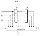
- Each of the primary-color-correlation horizontal interpolation circuit 26 and the primary-color-correlation vertical interpolation circuit 27 is basically constituted by a digital processing circuit composed of a block as shown in Fig. 19.
- Reference numerals 33 and 34 shown in Fig. 19 denote delay means comprising delay time equal to time required for one pixel to be transmitted, and reference numeral 35 denotes operation means.
- Each of the interpolation circuits 26 and 27 generates chrominance signals in three colors corresponding to the position of one pixel at the center of a block composed of 3 by 3 pixels on the basis of signals corresponding to the nine pixels in the block in this example.
- the signals L0, L1, and L2 outputted from the selection circuits 19, 20, and 21 are inputted to the delay means 33 and 34, whereby the signals corresponding to the nine pixels are simultaneously fed to the operation means 35. Interpolation processing is performed by the operation in the operation means 35.
- Fig. 20 illustrates the relationship between an arrangement of pixels on the CCD 1 and the selected pixels.
- line signals D1, D2, and D3 are first selected. Accordingly, a block composed of 3 by 3 pixels which are subjected to odd-numbered processing is as shown in Fig. 20 (b), and the pixels which are subjected to even-numbered processing are as shown in Fig. 20 (c).
- line signals D0, D1, and D2 are first selected. Accordingly, a block which is subjected to odd-numbered processing is as shown in Fig. 20 (d), and a block which is subjected to even-numbered processing is as shown in Fig. 20 (e).
- Fig. 21 illustrates an operation expression used by the horizontal interpolation circuit 26 and the vertical interpolation circuit 27 when a block to be processed is an odd-numbered block or an even-numbered block in an odd field.
- Gh, Bh, and Rh for a center pixel (a pixel to be processed) G22 are calculated in the following manner in the horizontal interpolation circuit 26.
- a signal G22 at the pixel to be processed G22 is used as it is as Gh for the pixel to be processed G22.
- Bh for the pixel to be processed G22 is found by calculating the average of signals B21 and B23 at two left and right pixels B21 and B23 with the pixel to be processed G22 interposed therebetween (utilizing a correlation in the horizontal direction).
- Rh for the pixel to be processed G22 becomes slightly complicated. That is, G12 which is a G signal at a pixel R12 is calculated as the average of G11 and G13 (i.e., utilizing a correlation in the horizontal direction) . Rh is found from the ratio of G12 found by calculation to G22 actually obtained and R12.
- Gv, Bv, and Rv for the center pixel (the pixel to be processed) G22 are calculated in the following manner in the horizontal interpolation circuit 27.
- the signal G22 for the pixel to be processed G22 is utilized as it is as Gv for the pixel to be processed G22.
- Rv for the pixel to be processed G22 is found by calculating the average of the signals R12 and R32 at upper and lower pixels R12 and R32 with the pixel to be processed G22 interposed therebetween (utilizing a correlation in the vertical direction).
- Bv for the pixel to be processed G22 is found, similarly to Rh, described above. That is, G21 which is a G signal at the pixel B21 is calculated as the average of G11 and G31 (utilizing a correlation in the vertical direction). Bv is calculated from the ratio of G21 found by calculation to G22 and B21.
- Gh, Bh, and Rh corresponding to a center pixel (a pixel to be processed) B22 are calculated in the following manner in the horizontal interpolation circuit 26.
- the signal B22 at the pixel to be processed B22 is used as it is as Bh for the pixel to be processed B22.
- Gh for the pixel to be processed B22 is found by calculating the average of the signals G21 and G23.
- Gv, Bv, and Rv for the center pixel (the pixel to be processed) B22 are calculated in the following manner in the vertical interpolation circuit 27.
- a signal B22 at the pixel to be processed B22 is used as it is with respect to Bv for the pixel to be processed B22.
- Gv for the pixel to be processed B22 is found by calculating the average of G12 and G32.
- Rv for the pixel to be processed B22 the average of R11 and R31 is first found to obtain R21.
- Each of the horizontal direction correlation detection circuit 23a and the vertical direction correlation detection circuit 23b is basically constituted by a digital processing circuit composed of a block as shown in Fig. 19.
- Reference numerals 33 and 34 shown in Fig. 19 denote delay means comprising delay time equal to time required for one pixel to be transmitted, and reference numeral 35 denotes operation means.
- the signals L0, L1, and L2 outputted from the selection circuits 19, 20, and 21 are inputted to the delay means 33 and 34, whereby signals corresponding to nine pixels are simultaneously fed to the operation means 35.
- Correlated value detection processing is performed by an operation in the operation means 35.
- Fig. 22 illustrates an operation expression used by the horizontal direction correlation detection circuit 23a and the vertical direction correlation detection circuit 23b.
- the correlated value detection circuits 23a and 23b respectively calculate the correlated values Sh and Sv utilizing G signals whose number is the largest in the block composed of 3 by 3 pixels.
- the vertical direction correlated value Sv is found by calculating the absolute value of the difference between G12 and G32. Since G12 and G13 do not actually exist, G12 is calculated from G11 and G13, and G32 is calculated from G31 and G33.
- the horizontal direction correlated value Sh in a case where the block to be processed is an odd-numbered block in the odd field is found by calculating the absolute value of the difference between G21 and G23. Since G21 and G23 do not actually exist, G21 is calculated from G11 and G31, and G23 is calculated from G13 and G33.
- the vertical direction correlated value Sv is found by calculating the absolute value of the difference between G12 and G32.
- the horizontal direction correlated value Sh is found by calculating the absolute value of the difference between G21 and G23.
- the pattern of the G signal is the same, whereby the same processing may be performed.
- the operation expression in a case where the block to be processed is an odd-numbered block in the odd field and the operation expression in a case where the block to be processed is an even-numbered block in the even field are the same.
- the operation expression in a case where the block to be processed is an even-numbered block in the odd field and the operation expression in a case where the block to be processed is an odd-numbered block in the even field are the same.
- the factor Kh in the horizontal direction becomes large when the correlation in the horizontal direction is smaller than the correlation in the vertical direction (Sh is smaller than Sv).
- the factor Kv in the vertical direction becomes large when the correlation in the vertical direction is smaller than the correlation in the horizontal direction (when Sv is smaller than Sh).
- the signal components of R, G, and B signals corresponding to one pixel in the CCD are calculated utilizing outputs from pixels (nine pixels in all) around the one pixel.
- an operation is executed using two methods, that is, a processing method suitable for a case where there is a strong correlation in the horizontal direction and a processing method suitable for a case where there is a strong correlation in the vertical direction.
- the results of the operation by the two methods are weighted and added depending on which of the horizontal correlation and the vertical correlation in the vicinity of the pixel is stronger.
- Fig. 23 (b) schematically illustrates the output level from each of the pixels. The reason why two types of output levels are illustrated differ in the color pattern, as described above, depending on the odd-numbered processing and the even-numbered processing.
- the levels of the signal components of the R, G, and B signals at the central position are all equal to 0.2.
- the color difference correlated color separator 25 and the above-mentioned primary color correlated color separator 24 differ from each other in the following points. That is, the interpolation processing in the primary color correlated color separator 24 utilizes the property of the ratio of the G signal to the R signal or the B signal being approximately equal between adjacent pixels because the local change of a chrominance signal is smaller than the change in luminance and the property of the ratio of a low-frequency component to a high-frequency component of a particular color component being also equal in the other color component.
- the interpolation processing in the color difference correlated color separator 25 utilizes the property of the difference between the G signal and the R signal or the B signal being approximately equal between adjacent pixels because the local change of a chrominance signal is small and the property of the difference between a low-frequency component and a high-frequency component of a particular color component being also equal in the other color component.
- Fig. 24 illustrates an operation expression used by the horizontal interpolation circuit 29 and the vertical interpolation circuit 30 in the color difference correlated color separator 25 when a block to be processed is an odd-numbered block or an even-numbered block in a odd field.
- Gh, Bh, and Rh for a center pixel (a pixel to be processed) G22 are calculated in the following manner in the horizontal interpolation circuit 29.
- a signal G22 at the pixel to be processed G22 is used as it is as Gh for the pixel to be processed G22.
- Bh for the pixel to be processed G22 is found by calculating the average of signals B21 and B23 at the two left and right pixels B21 and B23 with the pixel to be processed G22 interposed therebetween.
- Rh for the pixel to be processed G22 the property of the difference between the G signal and the R signal or the B signal being approximately equal between the adjacent pixels is utilized. That is, the following expression (4) holds:
- the horizontal interpolation circuit 29 performs the same operation, to find Gh, Rh, and Bh.
- a method of finding Gv, Rv, and Bv in the vertical interpolation circuit 30 is basically the same as that in interpolation processing by the horizontal interpolation circuit 29 and hence, the description thereof is not repeated.
- operation processing is occupied by multiplication and division.
- operation expression shown in Fig. 24 multiplication and division are replaced with addition and subtraction, and division for making a circuit arrangement particularly complicated is not used, thereby making it possible to significantly simplify the configuration of an operation processing circuit.
- the number of false chrominance signals is small with respect to an image close to a monotone image, thereby obtaining an image of high quality.
- the chrominance signals G1, R1, B1, G2, R2, and B2 outputted from the color separators 24 and 25, described above, are fed to a weighting and addition circuit 36 serving as synthesis means.
- the weighting and addition means 36 outputs final chrominance signals G0, R0, and B0.
- the chrominance signals G0, R0, and B0 outputted from the weighting and addition circuit 36 are fed to an AGC control circuit 37.
- the AGC control circuit 37 adjusts the degree of an aperture of an iris 1a from the chrominance signals G0, R0, and B0 or the gains of the AGCs 12 and 13 in order to control the luminance level of an image picked up.
- the iris 1a is basically controlled, to issue an instruction to reduce the gains of the AGCs when the aperture of the iris 1a increases to a maximum. At this time, an instruction to control the gains of the AGCs 12 and 13 is also fed to the weighting and addition circuit 36.
- the weighting and addition circuit 36 is so operated as to weight the chrominance signals G1, R1, and B1 from the primary color correlated color separator 24, weight the chrominance signals G2, R2, and B2 from the color difference correlated color separator 25, and add the weighted chrominance signals depending on the gains of the AGCs 12 and 13.
- the chrominance signals are added such that the chrominance signals G1, R1, and B1 are larger than the chrominance signals G2, R2, and B2 if the gains of the AGCs 12 and 13 are small, while being added such that the chrominance signals G2, R2, and B2 are larger than the chrominance signals G1, R1, and B1 if the gains are large, so that the chrominance signals G0, R0, and B0 are outputted.
- the chrominance signals are added such that the chrominance signals G1, R1, and B1 are larger than the chrominance signals G2, R2, and B2 if the gains of the AGCs 12 and 13 are small, while being added such that the chrominance signals G2, R2, and B2 are larger than the chrominance signals G1, R1, and B1 if the gains are large. Accordingly, it is possible to restrain the emphasis of noise included in an image produced by primary color correlated color separation processing and false colors included therein, and the resolution can be improved.
- an output of the primary color correlated color separator 24 and an output of the color difference correlated color separator 25 are weighted and added depending on the gains of the AGCs 12 and 13, the present invention is not limited to the same. For example, they may be weighted and added depending on the contrast of an image and the level of a signal.
- interpolation processing is performed in units of 3 by 3 pixels
- the present invention is not limited to the same.
- the interpolation processing is performed in units of 5 by 5 pixels, the false colors are further restrained, thereby making it possible to improve the resolution.
- the sixth embodiment differs from the fifth embodiment in terms of the operations of a primary-color-correlation horizontal interpolation circuit 26 and a primary-color-correlation vertical interpolation circuit 27 in a primary color correlated color separator 24. Further, the sixth embodiment differs from the fifth embodiment in terms of the operations of a color-difference-correlation horizontal interpolation circuit 29 and a color-difference-correlation vertical interpolation circuit 30 in a color difference correlated color separator 25.
- Each of interpolation circuits 26, 27, 29, and 30 produces chrominance signals in three colors corresponding to one pixel (a pixel to be processed) at the center on the basis of signals at 25 pixels in a block composed of 5 by 5 pixels in the sixth embodiment.
- the interpolation circuits 26 and 27 calculate chrominance signals R, G, and B at the pixel to be processed by a primary color correlated color separating system.
- Fig. 26 illustrates an operation expression used by the horizontal interpolation circuit 26 and the vertical interpolation circuit 27 in a case where the block to be processed is an odd-numbered block or an even-numbered block in an odd field.
- the operation of the vertical interpolation circuit 27 in a case where the block to be processed is an odd-numbered block in the odd field is taken as an example, to describe the primary color correlated color separating system.
- the direction in which the correlation of an image is strong in a local area is detected, to first calculate two low-frequency chrominance signals on the same line by filtering by lines in only the direction in which there is a strong correlation (here, the vertical direction or the horizontal direction).
- the signal G33 at the pixel to be processed G33 is used as it is.
- chrominance signals (R and G in this example) existing on a line to be an object can be color-separated from the respective one vertical and horizontal lines.
- Bv (B32/G32) ⁇ G33.
- Fig. 26 an expression obtained by expanding the simplified expression is described as Bv.
- filters for finding a low-frequency component of a signal used herein respectively have frequency characteristics as close to each other as possible.
- the tap length of the filter In order to match the filter characteristics of signals which differ in sampling phase, the tap length of the filter must be significantly lengthened, thereby significantly increasing the circuit scale, which is not practical.
- Rv, Gv, and Bv at the pixel to be processed can be found by the same operation even in a case where the block to be processed is an even-numbered block in the odd field.
- the primary color correlated color separating system exhibits good characteristics when the state of an input image is good, that is, input light is sufficient.
- the interpolation circuits 29 and 30 calculate chrominance signals R, G, and B at the pixel to be processed by a color difference correlated color separating system.
- Fig. 27 illustrates an operation expression used by the horizontal interpolation circuit 29 and the vertical interpolation circuit 30 in a case where the block to be processed is an odd-numbered block or an even-numbered block in an odd field.
- the operation of the vertical interpolation circuit 30 in a case where the block to be processed is an odd-numbered block in the odd field is taken as an example, to describe the color difference correlated color separating system.
- the direction in which a correlation of images is strong in a local area is detected utilizing a color difference correlation "the change in a color difference signal in a local area is small", to first calculate two low-frequency chrominance signals on the same line by filtering by lines in only the direction in which there is a strong correlation (here, the vertical direction or the horizontal direction).
- the signal G33 at the pixel to be processed G33 is used as it is.
- chrominance signals (R and G in this example) existing on a line to be an object can be color-separated from the respective one vertical and horizontal lines.
- the horizontal direction is the direction in which the correlation is low. Accordingly, the color difference signals at both the adjacent pixels in the horizontal direction are averaged, as expressed by the following expression (8), thereby compensating for the low correlation.
- B ⁇ [ ⁇ ( B 32- G 32)+( B 34- G 34))/2]+ G 33
- Bv (B32-G32) + G33.
- Fig. 27 an expression obtained by expanding the simplified expression is described as Bv.
- Rv, Gv, and Bv at the pixel to be processed can be found by the same operation even in a case where the block to be processed is an even-numbered block in the odd field.
- chrominance signals can be found only by addition and subtraction without performing division. Therefore, the system is characterized in that an error does not easily occur, and it also resists noise.
- the seventh embodiment differs from the fifth embodiment in terms of the operations of a primary-color-correlation horizontal interpolation circuit 26 and a primary-color-correlation vertical interpolation circuit 27 in a primary color correlated color separator 24. Further, the seventh embodiment differs from the fifth embodiment in terms of the operations of a color-difference-correlation horizontal interpolation circuit 29 and a color-difference-correlation vertical interpolation circuit 30 in a color difference correlated color separator 25.
- Each of the interpolation circuits 26, 27, 29 and 30 produces chrominance signals in three colors corresponding to one pixel (a pixel to be processed) at the center on the basis of signals at 25 pixels in a block composed of 5 by 5 pixels in the seventh embodiment.
- the color-difference-correlation horizontal interpolation circuit 29 and the color-difference-correlation vertical interpolation circuit 30 in the color difference correlated color separator 25 shown in Fig. 14 find chrominance signals R, G, and B at the pixel to be processed by a color difference correlated color separating system, as in the above-mentioned sixth embodiment.
- the primary color correlated color separator 24 shown in Fig. 14 is replaced with a color separator for finding chrominance signals R, G, and B at the pixel to be processed by an adaptive correlated color separating system (hereinafter referred to as an adaptive correlated color separator) in place of the primary color correlated color separator 24 shown in Fig. 14.
- the primary-color-correlation horizontal interpolation circuit 26 and the primary-color-correlation vertical interpolation circuit 27 in the adaptive correlated color separator 24 find chrominance signals R, G, and B at the pixel to be processed by the adaptive correlated color separating system 24.
- the interpolation circuits 26 and 27 calculate the chrominance signals R, G, and B at the pixel to be processed by the adaptive correlated color separating system.
- Fig. 28 illustrates an operation expression used by the primary-color-correlation horizontal interpolation circuit 26 and the primary-color-correlation vertical interpolation circuit 27 in the adaptive correlated color separator 24 in a case where the block to be processed is an odd-numbered block or an even-numbered block in an odd field.
- the operation of the vertical interpolation circuit 27 in a case where the block to be processed is an odd-numbered block in the odd field is taken as an example, to describe the adaptive correlated color separating system.
- the direction in which the correlation of an image is strong in a local area is detected, to first calculate two low-frequency chrominance signals on the same line by filtering by lines in only the direction in which there is a strong correlation (here, the vertical direction or the horizontal direction).
- the signal G33 for the pixel to be processed G33 is used as it is.
- chrominance signals (R and G in this example) existing on a line to be an object can be color-separated from the respective one vertical and horizontal lines.
- a method of finding Bv is the same as that in the primary color correlated color separating system.
- the horizontal direction is the direction in which the correlation is low. Accordingly, the color difference signals at both the adjacent pixels in the horizontal direction are averaged, as expressed by the following equation (9), thereby compensating for the low correlation.
- B ⁇ [ ⁇ (B32/G32) + (B34/G34) ⁇ /2] ⁇ G33
- Bv (B32/G32) ⁇ G33.
- Fig. 28 an expression obtained by expanding the simplified expression is described as Bv.
- Rv, Gv, and Bv at the pixel to be processed can be found by the same operation even in a case where the block to be processed is an even-numbered block in the odd field.
- the modified example is, of course, applicable to the second or seventh embodiment. For example, it is also applicable in the fifth embodiment.
- Used as the horizontal direction correlation detection means 23a and the vertical direction correlation detection means 23b in the correlation detection means 23 may be ones for calculating a horizontal direction correlated value Sh and a vertical direction correlated value Sv in the following manner.
- the horizontal direction correlation detection means 23a and the vertical direction correlation detection means 23b respectively calculate correlated values Sh and Sv corresponding to one pixel (a pixel to be processed) at the center on the basis of signals at 25 pixels in a block composed of 5 by 5 pixels.
- the correlated values Sh and Sv are calculated on the basis of the following expression (10)
- a dividing circuit may be able to be constituted by only a bit shift circuit by taking factors by which G33, B22, and B34 are respectively multiplexed as one in the foregoing expression (11) for calculating Sh and taking factors by which G33, R23, and R43 are respectively multiplexed as one in the expression for calculating Sv, to take the divisor in each of the expressions as eight which is the n-th power of 2.
- the ratios of the R, G, and B signals outputted from a CCD including color filters in a Mosaic arrangement differ depending on the color of a subject. Therefore, a disturbance is created depending on the color of the subject, so that the precision of the result of the judgment in the direction of a correlation using signals representing all pixels composing the CCD. Therefore, the intensity of the color of an input image is judged from the result of the integration of color difference signals in respective parts of a screen.
- the correlated values Sh and Sv are calculated on the basis of only the G signal.
- a dividing circuit may be able to be calculated by only a bit shift circuit by taking factors by which B33, G32, and G34 are respectively multiplexed as one in the foregoing expression (14) for calculating Sh and taking factors by which B33, G23, and G43 are respectively multiplexed as one in the expression for calculating Sv, to take the divisor in each of the expressions as eight which is the n-th power of 2.
- the correlated values Sh and Sv are calculated on the basis of the following expression (15) :
- the correlated values Sh and Sv may be calculated on the basis of the following expression (16), as in the fifth embodiment:
- the pattern of the G signal is the same, so that the same processing may be performed.
- An operation expression in a case where the block to be processed is an odd-numbered block in an odd field and an operation expression in a case where the block to be processed is an even-numbered block in an even field are the same, and an operation expression in a case where the block to be processed is an even-numbered block in an odd field and an operation expression in a case where the block to be processed is an odd-numbered block in an even field are the same.
- Sh1 and Sv1 be respectively correlated values calculated using operation expressions suitable for the case of an achromatic color (e.g., the foregoing expression (10)' or (13)'), and letting Sh2 and Sv2 calculated using operation expressions suitable for the case of a chromatic color (e.g., the foregoing expression (12)' or (15)'), the correlated values may be weighted and added depending on the intensity of the color of a block to be processed, to find correlated values Sh and Sv.
- an achromatic color e.g., the foregoing expression (10)' or (13)'
- Sh2 and Sv2 calculated using operation expressions suitable for the case of a chromatic color
- a chromatic color/achromatic color judged value R k corresponding to the chroma integrated value C k calculated by the foregoing expression (17) is found from the relationship between a chroma integrated value C k and the chromatic color/achromatic color judged value R k , as shown in Fig. 30.
- Two threshold values Th1 and Th2 in Fig. 30 are experimentally found because the characteristics of an optical LPF (Low-Pass Filter) indispensable in systematization are also related to the threshold values Th1 and Th2.
- the correlated values Sh1 and Sv1 calculated using the operation expression suitable for the case of the achromatic color and the correlated values Sh2 and Sv2 calculated using the operation expression suitable for the case of a chromatic color are weighted and added on the basis of the obtained chromatic color/achromatic color judged value R k , as expressed by the following expression:
- a judgment circuit 40 having L0, L1, and L2 as inputs and judging whether or not a pixel having a pixel value of zero is included in a block to be processed (the block to be processed composed of 3 by 3 pixels in the fifth embodiment, or the block to be processed composed of 5 by 5 pixels in the sixth embodiment) is provided, as shown in Fig. 31, in the fifth embodiment.
- the judgment circuit 40 outputs, when it judges that the pixel having a pixel value of zero is included in the block to be processed, a command to output only the chrominance signals calculated by the color difference correlated color separator 25 is outputted to the weighting and addition circuit 36.
- the same control is also carried out in the fifth embodiment.
- the result of the calculation increases to infinity when the divisor is zero, as in the primary color correlated color separator 24 shown in Fig. 14. Therefore, it is preferable that the same control is also carried out in the seventh embodiment,.
Landscapes
- Engineering & Computer Science (AREA)
- Multimedia (AREA)
- Signal Processing (AREA)
- Physics & Mathematics (AREA)
- Spectroscopy & Molecular Physics (AREA)
- Color Television Image Signal Generators (AREA)
- Solid State Image Pick-Up Elements (AREA)
- Processing Of Color Television Signals (AREA)
- Color Image Communication Systems (AREA)
Applications Claiming Priority (2)
| Application Number | Priority Date | Filing Date | Title |
|---|---|---|---|
| JP2000246488 | 2000-08-15 | ||
| JP2000246488A JP2002064831A (ja) | 2000-08-15 | 2000-08-15 | 単板式カラーカメラの色分離回路 |
Publications (2)
| Publication Number | Publication Date |
|---|---|
| EP1182891A2 true EP1182891A2 (de) | 2002-02-27 |
| EP1182891A3 EP1182891A3 (de) | 2005-02-02 |
Family
ID=18736788
Family Applications (1)
| Application Number | Title | Priority Date | Filing Date |
|---|---|---|---|
| EP01119518A Withdrawn EP1182891A3 (de) | 2000-08-15 | 2001-08-14 | Schaltung zur Farbtrennung in einer Farbkamera |
Country Status (3)
| Country | Link |
|---|---|
| US (1) | US20020041332A1 (de) |
| EP (1) | EP1182891A3 (de) |
| JP (1) | JP2002064831A (de) |
Cited By (2)
| Publication number | Priority date | Publication date | Assignee | Title |
|---|---|---|---|---|
| US8233733B2 (en) | 2007-04-05 | 2012-07-31 | Sony Corporation | Image processing device |
| EP1851971B1 (de) * | 2005-02-04 | 2015-09-23 | Qualcomm Incorporated | Adaptive farbinterpolation |
Families Citing this family (19)
| Publication number | Priority date | Publication date | Assignee | Title |
|---|---|---|---|---|
| JP2003234960A (ja) * | 2002-02-06 | 2003-08-22 | Sanyo Electric Co Ltd | 撮像装置 |
| US6995791B2 (en) * | 2002-04-02 | 2006-02-07 | Freescale Semiconductor, Inc. | Automatic white balance for digital imaging |
| US7456869B2 (en) * | 2003-05-27 | 2008-11-25 | Olympus Corporation | Imaging device and imaging device adjusting method |
| JP4497872B2 (ja) * | 2003-09-10 | 2010-07-07 | キヤノン株式会社 | 撮像装置 |
| JP3951993B2 (ja) * | 2003-09-11 | 2007-08-01 | カシオ計算機株式会社 | 撮像装置及びこの撮像装置に用いられるカラーデータ計測方法 |
| JP2006121612A (ja) * | 2004-10-25 | 2006-05-11 | Konica Minolta Photo Imaging Inc | 撮像装置 |
| JP4840740B2 (ja) * | 2004-12-01 | 2011-12-21 | 株式会社メガチップス | 画素補間方法および画像判定方法 |
| JP2007129581A (ja) * | 2005-11-04 | 2007-05-24 | Canon Inc | 撮像装置及び撮像システム |
| US7697046B2 (en) * | 2005-12-07 | 2010-04-13 | Hoya Corporation | Image signal processing device and method of image signal processing including pixel array pattern determination |
| KR100736366B1 (ko) * | 2006-02-02 | 2007-07-06 | 삼성전자주식회사 | 비디오 신호 처리 장치 및 방법 |
| JP5017597B2 (ja) * | 2007-11-27 | 2012-09-05 | 株式会社メガチップス | 画素補間方法 |
| US20100194915A1 (en) * | 2008-01-09 | 2010-08-05 | Peter Bakker | Method and apparatus for processing color values provided by a camera sensor |
| US8131110B2 (en) * | 2008-07-03 | 2012-03-06 | Seiko Epson Corporation | Reducing signal overshoots and undershoots in demosaicking |
| JP5414691B2 (ja) | 2008-11-21 | 2014-02-12 | 三菱電機株式会社 | 画像処理装置及び画像処理方法 |
| JP5624808B2 (ja) * | 2010-06-21 | 2014-11-12 | オリンパス株式会社 | 撮像装置 |
| JP2012010276A (ja) * | 2010-06-28 | 2012-01-12 | Sony Corp | 画像処理装置、画像処理方法及び画像処理プログラム |
| JP5539079B2 (ja) * | 2010-07-15 | 2014-07-02 | キヤノン株式会社 | 撮像装置、その制御方法及びプログラム |
| JP6276580B2 (ja) * | 2013-12-20 | 2018-02-07 | 株式会社メガチップス | 画素補間処理装置、撮像装置、プログラムおよび集積回路 |
| US10572743B1 (en) | 2017-08-28 | 2020-02-25 | Ambarella, Inc. | Real-time color classification for street vehicles |
Family Cites Families (9)
| Publication number | Priority date | Publication date | Assignee | Title |
|---|---|---|---|---|
| JPS61269484A (ja) * | 1985-05-24 | 1986-11-28 | Fuji Photo Film Co Ltd | カラ−ビデオカメラの自動ホワイトバランス調整装置 |
| JPS6489884A (en) * | 1987-09-30 | 1989-04-05 | Sony Corp | White balance correction circuit |
| US5420630A (en) * | 1992-09-11 | 1995-05-30 | Canon Kabushiki Kaisha | Image pickup apparatus performing white balance control based on data from regions of a frame |
| JP2931520B2 (ja) * | 1993-08-31 | 1999-08-09 | 三洋電機株式会社 | 単板式カラービデオカメラの色分離回路 |
| KR0130876B1 (ko) * | 1993-12-22 | 1998-04-22 | 구자홍 | 비데오 카메라의 자동 화이트 발란스장치 및 방법 |
| JP2816095B2 (ja) * | 1994-04-26 | 1998-10-27 | 三洋電機株式会社 | ビデオカメラの信号処理回路 |
| JP3787927B2 (ja) * | 1996-11-18 | 2006-06-21 | ソニー株式会社 | 撮像装置及びカラー画像信号の処理方法 |
| JP4269366B2 (ja) * | 1997-11-28 | 2009-05-27 | ソニー株式会社 | カメラ信号処理装置及びカメラ信号処理方法 |
| US6611287B1 (en) * | 1997-11-28 | 2003-08-26 | Sony Corporation | Camera signal processing apparatus and camera signal processing method |
-
2000
- 2000-08-15 JP JP2000246488A patent/JP2002064831A/ja active Pending
-
2001
- 2001-08-14 US US09/928,454 patent/US20020041332A1/en not_active Abandoned
- 2001-08-14 EP EP01119518A patent/EP1182891A3/de not_active Withdrawn
Cited By (2)
| Publication number | Priority date | Publication date | Assignee | Title |
|---|---|---|---|---|
| EP1851971B1 (de) * | 2005-02-04 | 2015-09-23 | Qualcomm Incorporated | Adaptive farbinterpolation |
| US8233733B2 (en) | 2007-04-05 | 2012-07-31 | Sony Corporation | Image processing device |
Also Published As
| Publication number | Publication date |
|---|---|
| JP2002064831A (ja) | 2002-02-28 |
| US20020041332A1 (en) | 2002-04-11 |
| EP1182891A3 (de) | 2005-02-02 |
Similar Documents
| Publication | Publication Date | Title |
|---|---|---|
| EP1182891A2 (de) | Schaltung zur Farbtrennung in einer Farbkamera | |
| JP2931520B2 (ja) | 単板式カラービデオカメラの色分離回路 | |
| US8125543B2 (en) | Solid-state imaging device and imaging apparatus with color correction based on light sensitivity detection | |
| US7466358B1 (en) | Solid-state imaging device for enlargement of dynamic range | |
| US9699429B2 (en) | Image processing apparatus, imaging device, image processing method, and program for reducing noise or false colors in an image | |
| US8149302B2 (en) | Method of processing noise in image data, noise reduction unit, and imaging apparatus | |
| JP4985584B2 (ja) | 撮像装置及び映像信号処理方法 | |
| CN102640500B (zh) | 图像处理设备 | |
| US6882754B2 (en) | Image signal processor with adaptive noise reduction and an image signal processing method therefor | |
| CN101494795B (zh) | 使用绿色光谱范围重叠的单位像素群的图像传感器及方法 | |
| US8013914B2 (en) | Imaging apparatus including noise suppression circuit | |
| US8792025B2 (en) | Image processing apparatus, image processing method, and solid-state imaging apparatus | |
| JP2011010108A (ja) | 撮像制御装置、撮像装置及び撮像制御方法 | |
| US8818108B2 (en) | Digital pixel addition method and device for processing plurality of images | |
| KR20070102399A (ko) | 촬상 장치 | |
| JP5167405B2 (ja) | 閃光の影響を補正する撮像装置 | |
| US6559886B1 (en) | Video signal processing method and device | |
| EP0910209A2 (de) | Eine Videkamera mit erweitertem Dynamikbereich | |
| KR19990063462A (ko) | 화상 신호 처리 장치 | |
| JP4043197B2 (ja) | 単板式カラーカメラの色分離回路 | |
| JP2008258909A (ja) | 信号処理回路 | |
| US20080037906A1 (en) | Image Pickup Device | |
| JP4600315B2 (ja) | カメラ装置の制御方法及びこれを用いたカメラ装置 | |
| JP2011114473A (ja) | 画素欠陥補正装置 | |
| JP2005311455A (ja) | 撮像装置、ノイズリダクション装置およびノイズリダクション方法並びにプログラム |
Legal Events
| Date | Code | Title | Description |
|---|---|---|---|
| PUAI | Public reference made under article 153(3) epc to a published international application that has entered the european phase |
Free format text: ORIGINAL CODE: 0009012 |
|
| AK | Designated contracting states |
Kind code of ref document: A2 Designated state(s): AT BE CH CY DE DK ES FI FR GB GR IE IT LI LU MC NL PT SE TR |
|
| AX | Request for extension of the european patent |
Free format text: AL;LT;LV;MK;RO;SI |
|
| PUAL | Search report despatched |
Free format text: ORIGINAL CODE: 0009013 |
|
| AK | Designated contracting states |
Kind code of ref document: A3 Designated state(s): AT BE CH CY DE DK ES FI FR GB GR IE IT LI LU MC NL PT SE TR |
|
| AX | Request for extension of the european patent |
Extension state: AL LT LV MK RO SI |
|
| 17P | Request for examination filed |
Effective date: 20050602 |
|
| AKX | Designation fees paid |
Designated state(s): DE FR GB |
|
| 17Q | First examination report despatched |
Effective date: 20060313 |
|
| STAA | Information on the status of an ep patent application or granted ep patent |
Free format text: STATUS: THE APPLICATION HAS BEEN WITHDRAWN |
|
| 18W | Application withdrawn |
Effective date: 20061128 |