EP1182425A1 - Dispositif d'essais de matériaux et son utilisation - Google Patents
Dispositif d'essais de matériaux et son utilisation Download PDFInfo
- Publication number
- EP1182425A1 EP1182425A1 EP01119025A EP01119025A EP1182425A1 EP 1182425 A1 EP1182425 A1 EP 1182425A1 EP 01119025 A EP01119025 A EP 01119025A EP 01119025 A EP01119025 A EP 01119025A EP 1182425 A1 EP1182425 A1 EP 1182425A1
- Authority
- EP
- European Patent Office
- Prior art keywords
- light
- test surface
- light source
- light guide
- probe
- Prior art date
- Legal status (The legal status is an assumption and is not a legal conclusion. Google has not performed a legal analysis and makes no representation as to the accuracy of the status listed.)
- Withdrawn
Links
Images
Classifications
-
- G—PHYSICS
- G01—MEASURING; TESTING
- G01N—INVESTIGATING OR ANALYSING MATERIALS BY DETERMINING THEIR CHEMICAL OR PHYSICAL PROPERTIES
- G01N21/00—Investigating or analysing materials by the use of optical means, i.e. using sub-millimetre waves, infrared, visible or ultraviolet light
- G01N21/17—Systems in which incident light is modified in accordance with the properties of the material investigated
- G01N21/25—Colour; Spectral properties, i.e. comparison of effect of material on the light at two or more different wavelengths or wavelength bands
- G01N21/31—Investigating relative effect of material at wavelengths characteristic of specific elements or molecules, e.g. atomic absorption spectrometry
Definitions
- the invention relates to a device for determining or Identification of the material of a test area by type of the main claim, as well as their use.
- thermoelectric principle there the test surfaces to be examined are contacted hot and cold, and the resulting one from the coating material dependent thermal voltage measured. Analyzers after the thermoelectric principle works almost non-destructively, however, it comes with the inevitable contact to deposits on the surfaces to be examined or contacts, so that such a device in the Routine control of surfaces can only be used to a limited extent is.
- the only non-destructive and non-contact Measuring method that was previously used in material detection is the X-ray fluorescence analysis, but with a relatively high expenditure on equipment and extensive Precautions against the occurrence of X-rays connected is.
- the object of the present invention was to provide a device with the non-destructive, non-contact and at the same time routinely on hard to reach and small surfaces a material test or material identification can be made.
- the device according to the invention has compared to the prior art Technology has the advantage that there is no destruction or impairment the test area to be analyzed comes. Further the proposed device is robust and also in series production without major investment or equipment Effort can be used. To that extent is the invention Device inexpensive, and it also enables 100% inspection of all components to be inspected, i.e. you does not have to be limited to random tests.
- Another advantage of the device according to the invention is the very short measurement time, which is typically below 200 msec. lies, and the fact that the measurement result immediately is available without complex evaluation procedures. Farther it is advantageous that the device according to the invention without moving parts gets along and easily fully into existing ones Production lines can be integrated. There is also no calibration required and there are almost no restrictions in terms of size and requirements the accessibility of the test area, since even with difficult to access Test areas only a correspondingly adapted one Probe must be used. To that extent is the invention Device for differentiating materials on plug contacts or connection surfaces of a large variety can be used by sensors or plugs.
- a probe is provided is the one hand with a light guide or a light guide bundle with the light source and on the other hand with one Optical fiber or an optical fiber bundle with the optical Spectrometer is connected.
- the Probe the incident light in a particularly simple way and at the same time with high intensity even inaccessible Areas or small test areas.
- the light source used is a has broadband emission spectrum, and especially in UV range as much as possible from a wavelength of 200 nm Light emitted.
- the optical Spectrometer uses the optical Spectrometer a wide range of wavelengths, in particular from 250 nm to 700 nm, analyzable.
- the invention is also suitable Device for the identification of aluminum or nickel, for example with nickel-plated aluminum contacts, or also for the detection of spark plug electrode materials.
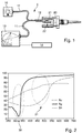
- Figure 1 shows a schematic diagram of a test device that shows Figure 2 one from the optical spectrometer in the wavelength range spectrum of the reflectivity recorded from 250 nm to 700 nm [%].
- Gold, silver and tin differ significantly in their spectral reflectivity.
- gold reflects blue-green light bad and therefore has the typical reddish-yellow color.
- Silver and tin show both a silvery-metallic in the visible frequency range Color, however, differ significantly in the ultraviolet Spectral range. So falls at a wavelength of about 320 nm the reflectivity of silver almost to zero, while the reflectivity of tin is not significant there changes. This effect is the one described below Device for distinguishing silver and Tin used.
- the spectral range from 400 nm to 500 nm used.
- a test device 5 is shown schematically in FIG. 1, in which a deuterium vapor lamp as the light source 10 serves.
- This light source 10 initially produces a broadband Spectrum using special, UV-transparent light guides 11 or corresponding optical fiber bundle to the one to be tested Surface is directed.
- the surface to be tested is a surface coating 22 of a plug connection 21, for example a flat plug tongue or a connector, in a connector 20, for example for a temperature sensor in a motor vehicle.
- the end of the light guide 11 is in the illustrated embodiment formed by a probe 12 which the light to the surface coating 22 inside the plug 20 passes.
- the light generated by the light source 10 occurs via a small one, mounted at an angle of 45 ° in the probe 12 Deflecting mirror at an angle of 90 ° from the Probe 12, and thus falls largely perpendicular to the Surface coating 22. That of the surface coating 22 and thus reflected from the coating material Light is then transmitted via a second light guide 11, for example a second glass fiber bundle, to an optical one Spectrometer 13 passed.
- a second light guide 11 for example a second glass fiber bundle
- a preferred embodiment of the invention provides that the light guides 11 each consist of a large number of individual Glass fibers exist that are statistically in the probe 12 mixed ends, so that always an optimal light output in the optical spectrometer 13 is guaranteed.
- the optical Spectrometer 13 can be a simple one in the illustrated example optical spectrometer that, for example, with a Computer as an evaluation unit 14 is connected.
- the Spectrometer 13 is used to record reflection spectra, i.e. the absorption of the reflectivity of the surface coating 22 as a test surface as a function of the wavelength, in the range from 250 nm to 700 nm.
- FIG. 2 shows three with the optical spectrometer 13 recorded spectra as a function of the wavelength in the range from 250 nm to 700 nm, the reflectivity the surface coating 22 applied as a test surface is.
- the evaluation unit 14 can easily determine which of the three coating materials Gold, silver or tin is present. So is evaluated by the evaluation unit 14 in a first area 30 300 nm to 350 nm compared to the identification of silver Made of tin or gold. This identification takes place especially due to the large increase in reflectivity in this wavelength range.
Applications Claiming Priority (2)
| Application Number | Priority Date | Filing Date | Title |
|---|---|---|---|
| DE2000142003 DE10042003B4 (de) | 2000-08-26 | 2000-08-26 | Materialprüfvorrichtung und deren Verwendung |
| DE10042003 | 2000-08-26 |
Publications (1)
| Publication Number | Publication Date |
|---|---|
| EP1182425A1 true EP1182425A1 (fr) | 2002-02-27 |
Family
ID=7653901
Family Applications (1)
| Application Number | Title | Priority Date | Filing Date |
|---|---|---|---|
| EP01119025A Withdrawn EP1182425A1 (fr) | 2000-08-26 | 2001-08-07 | Dispositif d'essais de matériaux et son utilisation |
Country Status (2)
| Country | Link |
|---|---|
| EP (1) | EP1182425A1 (fr) |
| DE (1) | DE10042003B4 (fr) |
Cited By (6)
| Publication number | Priority date | Publication date | Assignee | Title |
|---|---|---|---|---|
| CN100416260C (zh) * | 2003-05-16 | 2008-09-03 | 贵州虹山轴承总公司 | 检测镍合金元素及其含量的看谱分析方法 |
| EP2002228A2 (fr) * | 2006-03-22 | 2008-12-17 | ITT Manufacturing Enterprises, Inc. | Procede, appareil et systeme pour realiser une detection a distance, rapide et sensible, de contaminants de surface |
| WO2009040153A1 (fr) * | 2007-09-20 | 2009-04-02 | Robert Bosch Gmbh | Machine-outil |
| WO2013006955A1 (fr) | 2011-07-14 | 2013-01-17 | Kendall Technology Inc. | Procédé et appareil pour la détection d'or |
| US9188531B2 (en) | 2011-07-14 | 2015-11-17 | Kendall Technology Inc. | Method and apparatus for gold detection |
| FR3063144A1 (fr) | 2017-02-20 | 2018-08-24 | Robert Bosch Gmbh | Spectrometre et procede d'analyse d'un objet |
Families Citing this family (1)
| Publication number | Priority date | Publication date | Assignee | Title |
|---|---|---|---|---|
| DE10351666B3 (de) * | 2003-11-05 | 2005-01-27 | Erbslöh Aluminium Gmbh | Aluminiumprodukt |
Citations (6)
| Publication number | Priority date | Publication date | Assignee | Title |
|---|---|---|---|---|
| US5769540A (en) * | 1990-04-10 | 1998-06-23 | Luxtron Corporation | Non-contact optical techniques for measuring surface conditions |
| DE19721826A1 (de) * | 1997-05-26 | 1998-12-03 | Bosch Gmbh Robert | Vorrichtung und Verfahren zur Materialprüfung |
| JPH11326206A (ja) * | 1998-05-08 | 1999-11-26 | Nippon Steel Corp | 炉内溶融金属の光学的測定装置 |
| EP0965835A2 (fr) * | 1998-05-19 | 1999-12-22 | Hitachi, Ltd. | Capteur et appareil de mesure l'utilisant |
| US6069689A (en) * | 1997-04-16 | 2000-05-30 | Derma Technologies, Inc. | Apparatus and methods relating to optical systems for diagnosis of skin diseases |
| US6106662A (en) * | 1998-06-08 | 2000-08-22 | Speedfam-Ipec Corporation | Method and apparatus for endpoint detection for chemical mechanical polishing |
Family Cites Families (3)
| Publication number | Priority date | Publication date | Assignee | Title |
|---|---|---|---|---|
| DE4015066A1 (de) * | 1990-05-10 | 1991-11-14 | Hans Wilhelm Bergmann | Vorrichtung und verfahren zur automatischen kontrolle von zahnbehandlungen und chirurgischen eingriffen mit hilfe gepulster laser |
| IL109181A (en) * | 1994-03-31 | 1997-04-15 | Israel Atomic Energy Comm | Fiber optic reflectance probe |
| US5841546A (en) * | 1996-03-01 | 1998-11-24 | Foster-Miller, Inc. | Non-contact spectroscopy system and process |
-
2000
- 2000-08-26 DE DE2000142003 patent/DE10042003B4/de not_active Expired - Fee Related
-
2001
- 2001-08-07 EP EP01119025A patent/EP1182425A1/fr not_active Withdrawn
Patent Citations (6)
| Publication number | Priority date | Publication date | Assignee | Title |
|---|---|---|---|---|
| US5769540A (en) * | 1990-04-10 | 1998-06-23 | Luxtron Corporation | Non-contact optical techniques for measuring surface conditions |
| US6069689A (en) * | 1997-04-16 | 2000-05-30 | Derma Technologies, Inc. | Apparatus and methods relating to optical systems for diagnosis of skin diseases |
| DE19721826A1 (de) * | 1997-05-26 | 1998-12-03 | Bosch Gmbh Robert | Vorrichtung und Verfahren zur Materialprüfung |
| JPH11326206A (ja) * | 1998-05-08 | 1999-11-26 | Nippon Steel Corp | 炉内溶融金属の光学的測定装置 |
| EP0965835A2 (fr) * | 1998-05-19 | 1999-12-22 | Hitachi, Ltd. | Capteur et appareil de mesure l'utilisant |
| US6106662A (en) * | 1998-06-08 | 2000-08-22 | Speedfam-Ipec Corporation | Method and apparatus for endpoint detection for chemical mechanical polishing |
Non-Patent Citations (2)
| Title |
|---|
| HERRALA E ET AL: "IMAGING SPECTROMETER FOR PROCESS INDUSTRY APPLICATIONS", PROCEEDINGS OF THE SPIE, SPIE, BELLINGHAM, VA, US, vol. 2248, 1994, pages 33 - 40, XP000607543 * |
| PATENT ABSTRACTS OF JAPAN vol. 2000, no. 02 29 February 2000 (2000-02-29) * |
Cited By (12)
| Publication number | Priority date | Publication date | Assignee | Title |
|---|---|---|---|---|
| CN100416260C (zh) * | 2003-05-16 | 2008-09-03 | 贵州虹山轴承总公司 | 检测镍合金元素及其含量的看谱分析方法 |
| EP2002228A2 (fr) * | 2006-03-22 | 2008-12-17 | ITT Manufacturing Enterprises, Inc. | Procede, appareil et systeme pour realiser une detection a distance, rapide et sensible, de contaminants de surface |
| EP2002228A4 (fr) * | 2006-03-22 | 2010-05-26 | Itt Mfg Enterprises Inc | Procede, appareil et systeme pour realiser une detection a distance, rapide et sensible, de contaminants de surface |
| US7796251B2 (en) | 2006-03-22 | 2010-09-14 | Itt Manufacturing Enterprises, Inc. | Method, apparatus and system for rapid and sensitive standoff detection of surface contaminants |
| WO2009040153A1 (fr) * | 2007-09-20 | 2009-04-02 | Robert Bosch Gmbh | Machine-outil |
| JP2010538855A (ja) * | 2007-09-20 | 2010-12-16 | ローベルト ボツシユ ゲゼルシヤフト ミツト ベシユレンクテル ハフツング | 工作機械 |
| US8701534B2 (en) | 2007-09-20 | 2014-04-22 | Robert Bosch Gmbh | Machine tool |
| WO2013006955A1 (fr) | 2011-07-14 | 2013-01-17 | Kendall Technology Inc. | Procédé et appareil pour la détection d'or |
| EP2732264A1 (fr) * | 2011-07-14 | 2014-05-21 | Kendall Technology Inc. | Procédé et appareil pour la détection d'or |
| EP2732264A4 (fr) * | 2011-07-14 | 2015-03-11 | Kendall Technology Inc | Procédé et appareil pour la détection d'or |
| US9188531B2 (en) | 2011-07-14 | 2015-11-17 | Kendall Technology Inc. | Method and apparatus for gold detection |
| FR3063144A1 (fr) | 2017-02-20 | 2018-08-24 | Robert Bosch Gmbh | Spectrometre et procede d'analyse d'un objet |
Also Published As
| Publication number | Publication date |
|---|---|
| DE10042003B4 (de) | 2005-08-11 |
| DE10042003A1 (de) | 2002-03-21 |
Similar Documents
| Publication | Publication Date | Title |
|---|---|---|
| DE19856591C2 (de) | Vorrichtung zur spektroskopischen Analyse eines fluiden Mediums mittels abgeschwächter Reflexion | |
| CH654914A5 (de) | Optoelektronisches messverfahren und einrichtung zum bestimmen der oberflaechenguete streuend reflektierender oder transparenter oberflaechen. | |
| DE112017008060T5 (de) | Zubehörteil für ein Infrarot-Spektrometer | |
| EP0174496A2 (fr) | Méthode pour déterminer la longueur d'onde et la puissance de rayonnement de sources de lumière monochromatique avec correction de l'influence de la longueur d'onde et dispositif pour réaliser ce procédé | |
| DE10123470A1 (de) | Verfahren und Anordnung zur berührungslosen Ermittlung von Produkteigenschaften | |
| EP1182425A1 (fr) | Dispositif d'essais de matériaux et son utilisation | |
| DE102004021448B4 (de) | Spektrometrischer Reflexionsmesskopf und Verfahren zu dessen interner Rekalibrierung | |
| WO1992006366A1 (fr) | Dispositif pour la determination qualitative et/ou quantitative de la composition d'un echantillon a analyser | |
| EP1423676B8 (fr) | Dispositif de determination de proprietes rheologiques | |
| DE4312915A1 (de) | Verfahren und Anordnung zur IR-spektroskopischen Trennung von Kunststoffen | |
| DE3938142A1 (de) | Verfahren und vorrichtung zur qualitativen und quantitativen bestimmung von inhaltsstoffen | |
| EP2163883B1 (fr) | Appareil de mesure de grandeur de particules | |
| EP4133258B1 (fr) | Procédé et dispositif de détermination d'indices de réfraction dépendant de la fréquence | |
| DE19522188C2 (de) | Verfahren und Vorrichtung zur Bestimmung der Dicke und/oder des komplexen Brechungsindexes dünner Schichten und Verwendung zur Steuerung von Beschichtungsverfahren | |
| DE102004015946B3 (de) | Vorrichtung und Verfahren zur Raman-spektroskopischen Charakterisierung eines Prozessmediums | |
| DE3323313C2 (de) | Vorrichtung zur Echtheitsprüfung von Banknoten | |
| EP3770585B1 (fr) | Dispositif et procédé de mesure d'une concentration d'une substance dans un fluide | |
| EP0902273A2 (fr) | Procédé et appareil pour la détermination quantitative de suie | |
| DE10329205A1 (de) | Verfahren und Vorrichtung zum berührungslosen Bestimmen der Oberflächentemperatur eines Halbleiterwafers | |
| DE10128449B4 (de) | Vorrichtung und Verfahren zur Prüfung eines Materials | |
| DE19616245C2 (de) | Verfahren und Anordnung zum zerstörungsfreien, berührungslosen Prüfen und/oder Bewerten von Festkörpern, Flüssigkeiten, Gasen und Biomaterialien | |
| DE102006018287A1 (de) | Vorrichtung und Verfahren zur spektralanalytischen Bewertung von Materialien oder Objekten in einem Material- oder Objektstrom | |
| DE19608123A1 (de) | Spektrographisches Verfahren zur Bestimmung der absoluten Konzentration | |
| WO2006032496A1 (fr) | Element capteur atr | |
| WO2021175374A1 (fr) | Procédé de spectrométrie infrarouge et élément de réflexion associé et pièce |
Legal Events
| Date | Code | Title | Description |
|---|---|---|---|
| PUAI | Public reference made under article 153(3) epc to a published international application that has entered the european phase |
Free format text: ORIGINAL CODE: 0009012 |
|
| AK | Designated contracting states |
Kind code of ref document: A1 Designated state(s): AT BE CH CY DE DK ES FI FR GB GR IE IT LI LU MC NL PT SE TR |
|
| AX | Request for extension of the european patent |
Free format text: AL;LT;LV;MK;RO;SI |
|
| 17P | Request for examination filed |
Effective date: 20020827 |
|
| AKX | Designation fees paid |
Free format text: CH DE FR GB IT LI |
|
| 17Q | First examination report despatched |
Effective date: 20040312 |
|
| STAA | Information on the status of an ep patent application or granted ep patent |
Free format text: STATUS: THE APPLICATION IS DEEMED TO BE WITHDRAWN |
|
| 18D | Application deemed to be withdrawn |
Effective date: 20041209 |