EP1182425A1 - Material testing device and use thereof - Google Patents
Material testing device and use thereof Download PDFInfo
- Publication number
- EP1182425A1 EP1182425A1 EP01119025A EP01119025A EP1182425A1 EP 1182425 A1 EP1182425 A1 EP 1182425A1 EP 01119025 A EP01119025 A EP 01119025A EP 01119025 A EP01119025 A EP 01119025A EP 1182425 A1 EP1182425 A1 EP 1182425A1
- Authority
- EP
- European Patent Office
- Prior art keywords
- light
- test surface
- light source
- light guide
- probe
- Prior art date
- Legal status (The legal status is an assumption and is not a legal conclusion. Google has not performed a legal analysis and makes no representation as to the accuracy of the status listed.)
- Withdrawn
Links
Images
Classifications
-
- G—PHYSICS
- G01—MEASURING; TESTING
- G01N—INVESTIGATING OR ANALYSING MATERIALS BY DETERMINING THEIR CHEMICAL OR PHYSICAL PROPERTIES
- G01N21/00—Investigating or analysing materials by the use of optical means, i.e. using sub-millimetre waves, infrared, visible or ultraviolet light
- G01N21/17—Systems in which incident light is modified in accordance with the properties of the material investigated
- G01N21/25—Colour; Spectral properties, i.e. comparison of effect of material on the light at two or more different wavelengths or wavelength bands
- G01N21/31—Investigating relative effect of material at wavelengths characteristic of specific elements or molecules, e.g. atomic absorption spectrometry
Definitions
- the invention relates to a device for determining or Identification of the material of a test area by type of the main claim, as well as their use.
- thermoelectric principle there the test surfaces to be examined are contacted hot and cold, and the resulting one from the coating material dependent thermal voltage measured. Analyzers after the thermoelectric principle works almost non-destructively, however, it comes with the inevitable contact to deposits on the surfaces to be examined or contacts, so that such a device in the Routine control of surfaces can only be used to a limited extent is.
- the only non-destructive and non-contact Measuring method that was previously used in material detection is the X-ray fluorescence analysis, but with a relatively high expenditure on equipment and extensive Precautions against the occurrence of X-rays connected is.
- the object of the present invention was to provide a device with the non-destructive, non-contact and at the same time routinely on hard to reach and small surfaces a material test or material identification can be made.
- the device according to the invention has compared to the prior art Technology has the advantage that there is no destruction or impairment the test area to be analyzed comes. Further the proposed device is robust and also in series production without major investment or equipment Effort can be used. To that extent is the invention Device inexpensive, and it also enables 100% inspection of all components to be inspected, i.e. you does not have to be limited to random tests.
- Another advantage of the device according to the invention is the very short measurement time, which is typically below 200 msec. lies, and the fact that the measurement result immediately is available without complex evaluation procedures. Farther it is advantageous that the device according to the invention without moving parts gets along and easily fully into existing ones Production lines can be integrated. There is also no calibration required and there are almost no restrictions in terms of size and requirements the accessibility of the test area, since even with difficult to access Test areas only a correspondingly adapted one Probe must be used. To that extent is the invention Device for differentiating materials on plug contacts or connection surfaces of a large variety can be used by sensors or plugs.
- a probe is provided is the one hand with a light guide or a light guide bundle with the light source and on the other hand with one Optical fiber or an optical fiber bundle with the optical Spectrometer is connected.
- the Probe the incident light in a particularly simple way and at the same time with high intensity even inaccessible Areas or small test areas.
- the light source used is a has broadband emission spectrum, and especially in UV range as much as possible from a wavelength of 200 nm Light emitted.
- the optical Spectrometer uses the optical Spectrometer a wide range of wavelengths, in particular from 250 nm to 700 nm, analyzable.
- the invention is also suitable Device for the identification of aluminum or nickel, for example with nickel-plated aluminum contacts, or also for the detection of spark plug electrode materials.
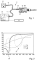
- Figure 1 shows a schematic diagram of a test device that shows Figure 2 one from the optical spectrometer in the wavelength range spectrum of the reflectivity recorded from 250 nm to 700 nm [%].
- Gold, silver and tin differ significantly in their spectral reflectivity.
- gold reflects blue-green light bad and therefore has the typical reddish-yellow color.
- Silver and tin show both a silvery-metallic in the visible frequency range Color, however, differ significantly in the ultraviolet Spectral range. So falls at a wavelength of about 320 nm the reflectivity of silver almost to zero, while the reflectivity of tin is not significant there changes. This effect is the one described below Device for distinguishing silver and Tin used.
- the spectral range from 400 nm to 500 nm used.
- a test device 5 is shown schematically in FIG. 1, in which a deuterium vapor lamp as the light source 10 serves.
- This light source 10 initially produces a broadband Spectrum using special, UV-transparent light guides 11 or corresponding optical fiber bundle to the one to be tested Surface is directed.
- the surface to be tested is a surface coating 22 of a plug connection 21, for example a flat plug tongue or a connector, in a connector 20, for example for a temperature sensor in a motor vehicle.
- the end of the light guide 11 is in the illustrated embodiment formed by a probe 12 which the light to the surface coating 22 inside the plug 20 passes.
- the light generated by the light source 10 occurs via a small one, mounted at an angle of 45 ° in the probe 12 Deflecting mirror at an angle of 90 ° from the Probe 12, and thus falls largely perpendicular to the Surface coating 22. That of the surface coating 22 and thus reflected from the coating material Light is then transmitted via a second light guide 11, for example a second glass fiber bundle, to an optical one Spectrometer 13 passed.
- a second light guide 11 for example a second glass fiber bundle
- a preferred embodiment of the invention provides that the light guides 11 each consist of a large number of individual Glass fibers exist that are statistically in the probe 12 mixed ends, so that always an optimal light output in the optical spectrometer 13 is guaranteed.
- the optical Spectrometer 13 can be a simple one in the illustrated example optical spectrometer that, for example, with a Computer as an evaluation unit 14 is connected.
- the Spectrometer 13 is used to record reflection spectra, i.e. the absorption of the reflectivity of the surface coating 22 as a test surface as a function of the wavelength, in the range from 250 nm to 700 nm.
- FIG. 2 shows three with the optical spectrometer 13 recorded spectra as a function of the wavelength in the range from 250 nm to 700 nm, the reflectivity the surface coating 22 applied as a test surface is.
- the evaluation unit 14 can easily determine which of the three coating materials Gold, silver or tin is present. So is evaluated by the evaluation unit 14 in a first area 30 300 nm to 350 nm compared to the identification of silver Made of tin or gold. This identification takes place especially due to the large increase in reflectivity in this wavelength range.
Abstract
Description
Die Erfindung betrifft eine Vorrichtung zur Bestimmung oder Identifikation des Materials einer Prüffläche nach der Gattung des Hauptanspruches, sowie deren Verwendung.The invention relates to a device for determining or Identification of the material of a test area by type of the main claim, as well as their use.
Bekannte Standardverfahren zur Identifikation des Materials einer Prüffläche sind zerstörend. So werden bei der elektrochemischen Analyse oder der Funkenerosionsspektroskopie zwar jeweils nur kleine Bereiche der zu prüfenden Oberfläche beschädigt, dies ist jedoch im Fall der Analyse der Oberfläche von Steckkontakten oder Anschlusskontaktflächen von beispielsweise Sensoren oder Steckern nicht vernachlässigbar, da sich in diesem Fall die zerstörende Prüfung auf einen für die Funktion dieser Bauteile besonders relevanten Bereich erstreckt. Weiter sind diese Verfahren auch bei Bauteilen bzw. zu prüfenden Oberflächen von geringer Größe oder Prüfoberflächen, die nur schwer zugänglich sind, vielfach nicht anwendbar.Known standard methods for identifying the material a test area are destructive. So with electrochemical Analysis or spark erosion spectroscopy though only small areas of the surface to be tested are damaged, however, this is in the case of surface analysis of plug contacts or connection contact surfaces of, for example Sensors or connectors not negligible, because in this case the destructive test is for one the function of these components particularly relevant area extends. These methods are also used for components or surfaces of small size to be tested or test surfaces, that are difficult to access, often not applicable.
Weitere Verfahren zur Prüfung der Zusammensetzung einer Oberfläche beruhen auf dem thermoelektrischen Prinzip. Dabei werden die zu untersuchenden Prüfflächen heiß und kalt kontaktiert, und die resultierende, vom Beschichtungsmaterial abhängige Thermospannung gemessen. Analysevorrichtungen nach dem thermoelektrischen Prinzip arbeiten zwar quasi zerstörungsfrei, es kommt jedoch bei der unvermeidbaren Kontaktierung zu Ablagerungen an den zu untersuchenden Oberflächen bzw. Kontakten, so dass auch eine solche Vorrichtung in der Routinekontrolle von Oberflächen nur eingeschränkt einsetzbar ist.Other procedures for checking the composition of a Surface are based on the thermoelectric principle. there the test surfaces to be examined are contacted hot and cold, and the resulting one from the coating material dependent thermal voltage measured. Analyzers after the thermoelectric principle works almost non-destructively, however, it comes with the inevitable contact to deposits on the surfaces to be examined or contacts, so that such a device in the Routine control of surfaces can only be used to a limited extent is.
Das einzige zerstörungsfreie und zugleich berührungslose Messverfahren, dass bisher in der Materialerkennung eingesetzt wird, ist die Röntgenfluororeszenzanalyse, die aber mit einem relativ hohen apparativen Aufwand und umfangreichen Schutzvorkehrungen vor der auftretenden Röntgenstrahlung verbunden ist.The only non-destructive and non-contact Measuring method that was previously used in material detection is the X-ray fluorescence analysis, but with a relatively high expenditure on equipment and extensive Precautions against the occurrence of X-rays connected is.
Aufgabe der vorliegenden Erfindung war die Bereitstellung einer Vorrichtung mit der zerstörungsfrei, berührungslos und gleichzeitig routinemäßig auch an schwer zugänglichen und kleinen Oberflächen eine Materialprüfung bzw. Materialidentifikation vorgenommen werden kann.The object of the present invention was to provide a device with the non-destructive, non-contact and at the same time routinely on hard to reach and small surfaces a material test or material identification can be made.
Die erfindungsgemäße Vorrichtung hat gegenüber dem Stand der Technik den Vorteil, dass es zu keiner Zerstörung bzw. Beeinträchtigung der zu analysierenden Prüffläche kommt. Weiter ist die vorgeschlagene Vorrichtung robust und auch in der Serienfertigung ohne großen Investitionsaufwand oder apparativen Aufwand einsetzbar. Insofern ist die erfindungsgemäße Vorrichtung kostengünstig, und sie ermöglicht zudem eine 100%ige Prüfung aller zu prüfenden Bauteile, d.h. man muss sich nicht auf stichprobenartige Prüfungen beschränken.The device according to the invention has compared to the prior art Technology has the advantage that there is no destruction or impairment the test area to be analyzed comes. Further the proposed device is robust and also in series production without major investment or equipment Effort can be used. To that extent is the invention Device inexpensive, and it also enables 100% inspection of all components to be inspected, i.e. you does not have to be limited to random tests.
Ein weiterer Vorteil der erfindungsgemäßen Vorrichtung ist die sehr kurze Messzeit, die typischerweise unterhalb von 200 msek. liegt, und die Tatsache, dass das Messergebnis sofort ohne aufwendige Auswerteverfahren vorliegt. Weiterhin ist vorteilhaft, dass die erfindungsgemäße Vorrichtung ohne bewegte Teile auskommt und problemlos voll in bestehende Fertigungslinien integrierbar ist. Weiter ist auch keine Kalibrierung erforderlich, und es bestehen nahezu keine Einschränkungen hinsichtlich der Größe und der Anforderungen an die Zugänglichkeit der Prüffläche, da selbst bei schwer zugänglichen Prüfflächen lediglich eine entsprechend angepasste Sonde eingesetzt werden muss. Insofern ist die erfindungsgemäße Vorrichtung zur Unterscheidung der Materialien auf Steckkontakten oder Anschlussflächen einer großen Vielzahl von Sensoren oder Steckern einsetzbar.Another advantage of the device according to the invention is the very short measurement time, which is typically below 200 msec. lies, and the fact that the measurement result immediately is available without complex evaluation procedures. Farther it is advantageous that the device according to the invention without moving parts gets along and easily fully into existing ones Production lines can be integrated. There is also no calibration required and there are almost no restrictions in terms of size and requirements the accessibility of the test area, since even with difficult to access Test areas only a correspondingly adapted one Probe must be used. To that extent is the invention Device for differentiating materials on plug contacts or connection surfaces of a large variety can be used by sensors or plugs.
Vorteilhafte Weiterbildungen der Erfindung ergeben sich aus den in den Unteransprüchen genannten Maßnahmen.Advantageous developments of the invention result from the measures specified in the subclaims.
So ist besonders vorteilhaft, wenn eine Sonde vorgesehen ist, die einerseits mit einem Lichtleiter oder einem Lichtleiterbündel mit der Lichtquelle und andererseits mit einem Lichtleiter oder einem Lichtleiterbündel mit dem optischen Spektrometer verbunden ist. Auf diese Weise kann über die Sonde das eingestrahlte Licht in besonders einfacher Weise und gleichzeitig mit hoher Intensität auch an unzugängliche Bereiche oder kleine Prüfflächen hingeführt werden.So it is particularly advantageous if a probe is provided is the one hand with a light guide or a light guide bundle with the light source and on the other hand with one Optical fiber or an optical fiber bundle with the optical Spectrometer is connected. In this way, the Probe the incident light in a particularly simple way and at the same time with high intensity even inaccessible Areas or small test areas.
Weiter ist vorteilhaft, wenn die eingesetzte Lichtquelle ein breitbandiges Emissionsspektrum hat, und besonders auch im UV-Bereich ab einer Wellenlänge von 200 nm möglichst viel Licht emittiert. In diesem Fall ist mit Hilfe des optischen Spektrometers ein großer Wellenlängenbereich, insbesondere von 250 nm bis 700 nm, analysierbar.It is also advantageous if the light source used is a has broadband emission spectrum, and especially in UV range as much as possible from a wavelength of 200 nm Light emitted. In this case, using the optical Spectrometer a wide range of wavelengths, in particular from 250 nm to 700 nm, analyzable.
Da als Beschichtungsmaterialien auf Steckkontakten oder Anschlusskontaktflächen vor allem Gold, Silber oder Zinn eingesetzt werden, ist vorteilhaft, dass sich diese Materialien in dem Wellenlängenbereich um 300 nm bzw. von 400 nm bis 550 nm in ihrem Reflexionsvermögen deutlich unterscheiden, so dass bei einem Auftrag der Intensität des von der Prüffläche reflektierten Lichtes als Funktion der Wellenlänge in dem Bereich von 250 nm bis 700 nm die Identifikation der Materialien Gold, Silber oder Zinn zuverlässig und einfach möglich ist. Weiter eignet sich die erfindungsgemäße Vorrichtung auch zur Identifikation von Aluminium oder Nikkel, beispielsweise bei vernickelten Aluminiumkontakten, oder auch zur Erkennung von Zündkerzenelektrodenmaterialien.Because as coating materials on plug contacts or connection contact surfaces mainly used gold, silver or tin it is advantageous that these materials in the wavelength range around 300 nm or from 400 nm to Clearly distinguish 550 nm in their reflectivity, so with an order the intensity of the of the Test surface of reflected light as a function of the wavelength identification in the range from 250 nm to 700 nm of the materials gold, silver or tin reliable and simple is possible. The invention is also suitable Device for the identification of aluminum or nickel, for example with nickel-plated aluminum contacts, or also for the detection of spark plug electrode materials.
Die Erfindung wird anhand der Zeichnungen und in der nachfolgenden Beschreibung näher erläutert. Die Figur 1 zeigt eine Prinzipskizze einer Prüfvorrichtung, die Figur 2 zeigt ein von dem optischen Spektrometer im Wellenlängenbereich von 250 nm bis 700 nm aufgenommenes Spektrum des Reflexionsvermögens [%].The invention is illustrated in the drawings and in the following Description explained in more detail. Figure 1 shows a schematic diagram of a test device that shows Figure 2 one from the optical spectrometer in the wavelength range spectrum of the reflectivity recorded from 250 nm to 700 nm [%].
Gold, Silber und Zinn unterscheiden sich wesentlich in ihrem spektralen Reflexionsvermögen. So reflektiert Gold beispielsweise blau-grünes Licht schlecht und hat daher die typisch rötlich-gelbe Farbe. Silber und Zinn hingegen zeigen im sichtbaren Frequenzbereich beide eine silbrig-metallische Farbe, unterscheiden sich jedoch deutlich im ultravioletten Spektralbereich. So fällt bei einer Wellenlänge von etwa 320 nm das Reflexionsvermögen von Silber nahezu auf null, während sich das Reflexionsvermögen von Zinn dort nicht signifikant ändert. Dieser Effekt wird bei der nachfolgend beschriebenen Vorrichtung zur Unterscheidung von Silber und Zinn ausgenutzt. Für die Erkennung von Gold und die Unterscheidung von Gold gegenüber Silber oder Zinn wird der Spektralbereich von 400 nm bis 500 nm eingesetzt. Gold, silver and tin differ significantly in their spectral reflectivity. For example, gold reflects blue-green light bad and therefore has the typical reddish-yellow color. Silver and tin, however, show both a silvery-metallic in the visible frequency range Color, however, differ significantly in the ultraviolet Spectral range. So falls at a wavelength of about 320 nm the reflectivity of silver almost to zero, while the reflectivity of tin is not significant there changes. This effect is the one described below Device for distinguishing silver and Tin used. For the detection of gold and the differentiation from gold to silver or tin becomes the spectral range from 400 nm to 500 nm used.
In Figur 1 ist schematisch eine Prüfvorrichtung 5 dargestellt,
bei der eine Deuteriumdampf-Lampe als Lichtquelle 10
dient. Diese Lichtquelle 10 erzeugt zunächst ein breitbandiges
Spektrum, das über spezielle, UV-transparente Lichtleiter
11 oder entsprechende Lichtleiterbündel zu der zu prüfenden
Oberfläche hingeleitet wird. Im erläuterten Beispiel
ist die zu prüfende Oberfläche eine Oberflächenbeschichtung
22 einer Steckverbindung 21, beispielsweise eine Flachstekkerzunge
oder ein Steckverbinder, in einem Stecker 20, beispielsweise
für einen Temperaturfühler in einem Kraftfahrzeug.
Das Ende des Lichtleiters 11 wird im erläuterten Ausführungsbeispiel
von einer Sonde 12 gebildet, die das Licht
zu der Oberflächenbeschichtung 22 im Inneren des Steckers 20
leitet. Dort tritt das von der Lichtquelle 10 erzeugte Licht
über einen kleinen, im Winkel von 45° in der Sonde 12 montierten
Umlenkspiegel unter einem Winkel von 90° aus der
Sonde 12 aus, und fällt somit weitgehend senkrecht auf die
Oberflächenbeschichtung 22. Das von der Oberflächenbeschichtung
22 und damit vom Beschichtungsmaterial reflektierte
Licht wird dann im Weiteren über einen zweiten Lichtleiter
11, beispielsweise ein zweites Glasfaserbündel, zu einem optischen
Spektrometer 13 geleitet.A
Eine bevorzugte Ausführungsform der Erfindung sieht vor,
dass die Lichtleiter 11 jeweils aus einer Vielzahl von einzelnen
Glasfasern bestehen, die in der Sonde 12 statistisch
gemischt enden, so dass stets eine optimale Lichtausbeute im
optischen Spektrometer 13 gewährleistet ist. Das optische
Spektrometer 13 kann im erläuterten Beispiel ein einfaches
optisches Spektrometer sein, dass beispielsweise mit einem
Computer als Auswerteeinheit 14 in Verbindung steht. Das
Spektrometer 13 dient der Aufnahme von Reflexionsspektren,
d.h. der Aufnahme des Reflexionsvermögens der Oberflächenbeschichtung
22 als Prüffläche als Funktion der Wellenlänge,
im Bereich von 250 nm bis 700 nm. A preferred embodiment of the invention provides
that the
Die Figur 2 zeigt drei mit dem optischen Spektrometer 13
aufgenommene Spektren als Funktion der Wellenlänge im Bereich
von 250 nm bis 700 nm, wobei das Reflexionsvermögen
der Oberflächenbeschichtung 22 als Prüffläche aufgetragen
ist. Im Einzelnen sind in Figur 2 drei Spektren für die Materialien
Gold, Silber und Zinn als Oberflächenbeschichtung
22 zusammengefasst. Anhand des relativen Verlaufs dieser
drei Spektren ist klar ersichtlich, und mit der Auswerteeinheit
14 in einfacher Weise bestimmbar, welches der drei Beschichtungsmaterialien
Gold, Silber oder Zinn vorliegt. So
wird durch die Auswerteeinheit 14 in einem ersten Bereich 30
von ca. 300 nm bis 350 nm die Identifikation von Silber gegenüber
Zinn oder Gold vorgenommen. Diese Identifikation erfolgt
insbesondere durch den großen Anstieg des Reflexionsvermögens
in diesem Wellenlängenbereich. Liegt kein Silber
vor, wird weiter dann über die Änderung des Reflexionsvermögens
im Wellenlängenbereich von 400 nm bis 500 nm, der in
Figur 2 als zweiter Bereich 31 gekennzeichnet ist, Gold von
Zinn unterschieden. Insbesondere weist Gold in diesem Längenwellenbereich
eine deutlich größere Änderung des Reflexionsvermögens
als Funktion der Wellenlänge auf als Zinn.FIG. 2 shows three with the
Die Auswertung der relativen Verläufe der Reflexionsspektren
macht im Übrigen die vorgeschlagene Prüfvorrichtung 5 und
das eingesetzte Verfahren unabhängig von der Oberflächenrauhigkeit
der Oberflächenbeschichtung 22, die zwischen einzelnen
Chargen von Steckern bzw. Sonden stark variieren kann.
Weiterhin spielen auch leichte Verunreinigungen der zu prüfenden
Oberfläche keine Rolle. Zudem sei betont, dass die
erläuterte Prüfvorrichtung 5 auch zur Unterscheidung von anderen
Metallen geeignet ist.The evaluation of the relative courses of the reflection spectra
otherwise makes the proposed
Claims (9)
Applications Claiming Priority (2)
| Application Number | Priority Date | Filing Date | Title |
|---|---|---|---|
| DE2000142003 DE10042003B4 (en) | 2000-08-26 | 2000-08-26 | Material testing device and its use |
| DE10042003 | 2000-08-26 |
Publications (1)
| Publication Number | Publication Date |
|---|---|
| EP1182425A1 true EP1182425A1 (en) | 2002-02-27 |
Family
ID=7653901
Family Applications (1)
| Application Number | Title | Priority Date | Filing Date |
|---|---|---|---|
| EP01119025A Withdrawn EP1182425A1 (en) | 2000-08-26 | 2001-08-07 | Material testing device and use thereof |
Country Status (2)
| Country | Link |
|---|---|
| EP (1) | EP1182425A1 (en) |
| DE (1) | DE10042003B4 (en) |
Cited By (6)
| Publication number | Priority date | Publication date | Assignee | Title |
|---|---|---|---|---|
| CN100416260C (en) * | 2003-05-16 | 2008-09-03 | 贵州虹山轴承总公司 | Spectroscopic analysis method of detecting nickel alloy element and its content |
| EP2002228A2 (en) * | 2006-03-22 | 2008-12-17 | ITT Manufacturing Enterprises, Inc. | Method, apparatus and system for rapid and sensitive standoff detection of surface contaminants |
| WO2009040153A1 (en) * | 2007-09-20 | 2009-04-02 | Robert Bosch Gmbh | Machine tool |
| WO2013006955A1 (en) | 2011-07-14 | 2013-01-17 | Kendall Technology Inc. | Method and apparatus for gold detection |
| US9188531B2 (en) | 2011-07-14 | 2015-11-17 | Kendall Technology Inc. | Method and apparatus for gold detection |
| FR3063144A1 (en) | 2017-02-20 | 2018-08-24 | Robert Bosch Gmbh | SPECTROMETER AND METHOD FOR ANALYZING AN OBJECT |
Families Citing this family (1)
| Publication number | Priority date | Publication date | Assignee | Title |
|---|---|---|---|---|
| DE10351666B3 (en) * | 2003-11-05 | 2005-01-27 | Erbslöh Aluminium Gmbh | Aluminum product for the inner and outer parts of vehicles is made from an aluminum alloy containing alloying additions of magnesium and silicon |
Citations (6)
| Publication number | Priority date | Publication date | Assignee | Title |
|---|---|---|---|---|
| US5769540A (en) * | 1990-04-10 | 1998-06-23 | Luxtron Corporation | Non-contact optical techniques for measuring surface conditions |
| DE19721826A1 (en) * | 1997-05-26 | 1998-12-03 | Bosch Gmbh Robert | Device for material testing of electrically conducting material, especially lug contact |
| JPH11326206A (en) * | 1998-05-08 | 1999-11-26 | Nippon Steel Corp | Optical measuring instrument for molten metal in furnace |
| EP0965835A2 (en) * | 1998-05-19 | 1999-12-22 | Hitachi, Ltd. | Sensor and measuring apparatus using the same |
| US6069689A (en) * | 1997-04-16 | 2000-05-30 | Derma Technologies, Inc. | Apparatus and methods relating to optical systems for diagnosis of skin diseases |
| US6106662A (en) * | 1998-06-08 | 2000-08-22 | Speedfam-Ipec Corporation | Method and apparatus for endpoint detection for chemical mechanical polishing |
Family Cites Families (3)
| Publication number | Priority date | Publication date | Assignee | Title |
|---|---|---|---|---|
| DE4015066A1 (en) * | 1990-05-10 | 1991-11-14 | Hans Wilhelm Bergmann | Automatically controlling dental treatment and surgery - using simultaneous spectrometer and computer to measure spectral reflectivity of tooth surface subjected to pulsed laser via optical frame |
| IL109181A (en) * | 1994-03-31 | 1997-04-15 | Israel Atomic Energy Comm | Fiber optic reflectance probe |
| US5841546A (en) * | 1996-03-01 | 1998-11-24 | Foster-Miller, Inc. | Non-contact spectroscopy system and process |
-
2000
- 2000-08-26 DE DE2000142003 patent/DE10042003B4/en not_active Expired - Fee Related
-
2001
- 2001-08-07 EP EP01119025A patent/EP1182425A1/en not_active Withdrawn
Patent Citations (6)
| Publication number | Priority date | Publication date | Assignee | Title |
|---|---|---|---|---|
| US5769540A (en) * | 1990-04-10 | 1998-06-23 | Luxtron Corporation | Non-contact optical techniques for measuring surface conditions |
| US6069689A (en) * | 1997-04-16 | 2000-05-30 | Derma Technologies, Inc. | Apparatus and methods relating to optical systems for diagnosis of skin diseases |
| DE19721826A1 (en) * | 1997-05-26 | 1998-12-03 | Bosch Gmbh Robert | Device for material testing of electrically conducting material, especially lug contact |
| JPH11326206A (en) * | 1998-05-08 | 1999-11-26 | Nippon Steel Corp | Optical measuring instrument for molten metal in furnace |
| EP0965835A2 (en) * | 1998-05-19 | 1999-12-22 | Hitachi, Ltd. | Sensor and measuring apparatus using the same |
| US6106662A (en) * | 1998-06-08 | 2000-08-22 | Speedfam-Ipec Corporation | Method and apparatus for endpoint detection for chemical mechanical polishing |
Non-Patent Citations (2)
| Title |
|---|
| HERRALA E ET AL: "IMAGING SPECTROMETER FOR PROCESS INDUSTRY APPLICATIONS", PROCEEDINGS OF THE SPIE, SPIE, BELLINGHAM, VA, US, vol. 2248, 1994, pages 33 - 40, XP000607543 * |
| PATENT ABSTRACTS OF JAPAN vol. 2000, no. 02 29 February 2000 (2000-02-29) * |
Cited By (12)
| Publication number | Priority date | Publication date | Assignee | Title |
|---|---|---|---|---|
| CN100416260C (en) * | 2003-05-16 | 2008-09-03 | 贵州虹山轴承总公司 | Spectroscopic analysis method of detecting nickel alloy element and its content |
| EP2002228A2 (en) * | 2006-03-22 | 2008-12-17 | ITT Manufacturing Enterprises, Inc. | Method, apparatus and system for rapid and sensitive standoff detection of surface contaminants |
| EP2002228A4 (en) * | 2006-03-22 | 2010-05-26 | Itt Mfg Enterprises Inc | Method, apparatus and system for rapid and sensitive standoff detection of surface contaminants |
| US7796251B2 (en) | 2006-03-22 | 2010-09-14 | Itt Manufacturing Enterprises, Inc. | Method, apparatus and system for rapid and sensitive standoff detection of surface contaminants |
| WO2009040153A1 (en) * | 2007-09-20 | 2009-04-02 | Robert Bosch Gmbh | Machine tool |
| JP2010538855A (en) * | 2007-09-20 | 2010-12-16 | ローベルト ボツシユ ゲゼルシヤフト ミツト ベシユレンクテル ハフツング | Machine Tools |
| US8701534B2 (en) | 2007-09-20 | 2014-04-22 | Robert Bosch Gmbh | Machine tool |
| WO2013006955A1 (en) | 2011-07-14 | 2013-01-17 | Kendall Technology Inc. | Method and apparatus for gold detection |
| EP2732264A1 (en) * | 2011-07-14 | 2014-05-21 | Kendall Technology Inc. | Method and apparatus for gold detection |
| EP2732264A4 (en) * | 2011-07-14 | 2015-03-11 | Kendall Technology Inc | Method and apparatus for gold detection |
| US9188531B2 (en) | 2011-07-14 | 2015-11-17 | Kendall Technology Inc. | Method and apparatus for gold detection |
| FR3063144A1 (en) | 2017-02-20 | 2018-08-24 | Robert Bosch Gmbh | SPECTROMETER AND METHOD FOR ANALYZING AN OBJECT |
Also Published As
| Publication number | Publication date |
|---|---|
| DE10042003A1 (en) | 2002-03-21 |
| DE10042003B4 (en) | 2005-08-11 |
Similar Documents
| Publication | Publication Date | Title |
|---|---|---|
| DE19856591C2 (en) | Device for the spectroscopic analysis of a fluid medium by means of attenuated reflection | |
| CH654914A5 (en) | OPTOELECTRONIC MEASURING METHOD AND DEVICE FOR DETERMINING THE SURFACE QUALITY REFLECTIVELY REFLECTING OR TRANSPARENT SURFACES. | |
| DE112017008060T5 (en) | Accessory for an infrared spectrometer | |
| EP0174496A2 (en) | Procedure for measuring the radiation wavelength and the wavelength-corrected radiation power of monochromatical light-sources and arrangement for carrying out this procedure | |
| DE10123470A1 (en) | Acquiring geometric and optical properties of the different layers of a layer system comprises using a measuring device and measuring methods for acquiring the properties of one of the layers | |
| EP1182425A1 (en) | Material testing device and use thereof | |
| DE102004021448B4 (en) | Spectrometric reflection probe and method for its internal recalibration | |
| WO1992006366A1 (en) | Device for the qualitative and/or quantitative determination of the compositon of a sample to be analysed | |
| EP1423676B8 (en) | Device for determining rheological properties | |
| DE4312915A1 (en) | Process and arrangement for the IR (infrared) spectroscopic separation of plastics | |
| EP2163883B1 (en) | Particle size measuring device | |
| EP4133258B1 (en) | Method and device for determining frequency-dependent refractive indices | |
| DE19522188C2 (en) | Method and device for determining the thickness and / or the complex refractive index of thin layers and use for controlling coating processes | |
| DE102004015946B3 (en) | Raman spectrum generation and detection unit couples light into medium through optical fibre without focussing | |
| DE3323313C2 (en) | Device for checking the authenticity of banknotes | |
| EP3770585B1 (en) | Device and method for detecting a concentration of a substance in a fluid | |
| EP0902273A2 (en) | Method and apparatus for quantitative determination of soot | |
| DE10329205A1 (en) | Contactless measurement of the surface temperature of a semiconductor wafer by measuring the surface radiating intensity at two wavelengths having the same emission ratio and then formation of their quotient | |
| DE10128449B4 (en) | Device and method for testing a material | |
| DE19616245C2 (en) | Method and arrangement for non-destructive, non-contact testing and / or evaluation of solids, liquids, gases and biomaterials | |
| DE102006018287A1 (en) | Spectrometer for evaluating e.g. paper, has halogen lamps strung in line in defined distances and transverse to material or object stream, and light receiving optics arranged such that optic axis lies in symmetrical plane of light radiation | |
| DE19608123A1 (en) | Spectroscopic method to determine absolute concentration of substance | |
| WO2006032496A1 (en) | Atr sensor element | |
| WO2021175374A1 (en) | Ir spectrometric method, associated reflection element and component | |
| DE19526943A1 (en) | Multiple reflector for spectrometric detection of absorbed substances over greater distances or quantities - uses cylindrical and opposing concave mirrors, and measures conventional or multipath saturated fluorescence |
Legal Events
| Date | Code | Title | Description |
|---|---|---|---|
| PUAI | Public reference made under article 153(3) epc to a published international application that has entered the european phase |
Free format text: ORIGINAL CODE: 0009012 |
|
| AK | Designated contracting states |
Kind code of ref document: A1 Designated state(s): AT BE CH CY DE DK ES FI FR GB GR IE IT LI LU MC NL PT SE TR |
|
| AX | Request for extension of the european patent |
Free format text: AL;LT;LV;MK;RO;SI |
|
| 17P | Request for examination filed |
Effective date: 20020827 |
|
| AKX | Designation fees paid |
Free format text: CH DE FR GB IT LI |
|
| 17Q | First examination report despatched |
Effective date: 20040312 |
|
| STAA | Information on the status of an ep patent application or granted ep patent |
Free format text: STATUS: THE APPLICATION IS DEEMED TO BE WITHDRAWN |
|
| 18D | Application deemed to be withdrawn |
Effective date: 20041209 |