EP1179737B1 - Anordnung zum Testen eines integrierten Schaltkreises - Google Patents
Anordnung zum Testen eines integrierten Schaltkreises Download PDFInfo
- Publication number
- EP1179737B1 EP1179737B1 EP01000351A EP01000351A EP1179737B1 EP 1179737 B1 EP1179737 B1 EP 1179737B1 EP 01000351 A EP01000351 A EP 01000351A EP 01000351 A EP01000351 A EP 01000351A EP 1179737 B1 EP1179737 B1 EP 1179737B1
- Authority
- EP
- European Patent Office
- Prior art keywords
- circuit
- test
- signal
- clock signals
- software
- Prior art date
- Legal status (The legal status is an assumption and is not a legal conclusion. Google has not performed a legal analysis and makes no representation as to the accuracy of the status listed.)
- Expired - Lifetime
Links
Images

Classifications
-
- G—PHYSICS
- G01—MEASURING; TESTING
- G01R—MEASURING ELECTRIC VARIABLES; MEASURING MAGNETIC VARIABLES
- G01R31/00—Arrangements for testing electric properties; Arrangements for locating electric faults; Arrangements for electrical testing characterised by what is being tested not provided for elsewhere
- G01R31/28—Testing of electronic circuits, e.g. by signal tracer
- G01R31/317—Testing of digital circuits
- G01R31/3181—Functional testing
- G01R31/3185—Reconfiguring for testing, e.g. LSSD, partitioning
-
- G—PHYSICS
- G01—MEASURING; TESTING
- G01R—MEASURING ELECTRIC VARIABLES; MEASURING MAGNETIC VARIABLES
- G01R31/00—Arrangements for testing electric properties; Arrangements for locating electric faults; Arrangements for electrical testing characterised by what is being tested not provided for elsewhere
- G01R31/28—Testing of electronic circuits, e.g. by signal tracer
- G01R31/317—Testing of digital circuits
- G01R31/3181—Functional testing
- G01R31/3185—Reconfiguring for testing, e.g. LSSD, partitioning
- G01R31/318533—Reconfiguring for testing, e.g. LSSD, partitioning using scanning techniques, e.g. LSSD, Boundary Scan, JTAG
- G01R31/318552—Clock circuits details
Definitions
- the invention relates to an arrangement for testing an integrated circuit, which has at least two circuit parts which in normal operation with at least two different clock signals work.
- the integrated circuit to be tested is designed such that in that each of the clock signals can be switched on and off individually by a test software provided in the arrangement in a test mode in that a software model of the circuit under test is provided in the arrangement, in which an X generator is provided for those circuit parts whose operation is influenced by a plurality of clock signals and their edge uncertainties, which is then activated and delivers an X signal, if Testing more than one of the operation of the circuit part influencing clock signals is activated, that the test software first activates all the clock signals during testing and evaluates test results for those circuit parts for which no X signal appears in the software model, and that the test software performs a plurality of test runs for those circuit parts for which an X signal appeared in the software model when testing with all clock signals, in which only one or more of the clock signals influencing the operation of the circuit part is activated, and only those tests evaluates the circuit parts of the circuit for which no X signal appears in the software model.
- the test arrangement For the test arrangement according to the invention, the following basic method of operation applies: On the one hand there is a real integrated circuit, which is to be tested by means provided in the arrangement hardware, in which so outside of the circuit occurring signals are tapped and checked whether they with the Set behavior of the circuit match. Parallel to this, there exists a software model of the circuit to be tested from which, on the one hand, the desired behavior is known and, on the other hand, serves to determine in a manner to be described below which circuit parts of the circuit can be tested with several simultaneously activated clock signals.
- the inventive arrangement for testing an integrated circuit requires that it is designed such that each of the clock signals that is used in the integrated circuit is individually switched on and off by a test software provided externally in the arrangement in the test mode. It should therefore be possible to switch the individual clock signals on or off as required by means of the test software, it also being possible to activate several clock signals simultaneously if necessary.
- a software model of the circuit present in the integrated circuit is provided and is to be tested.
- the software model is designed to be suitable for such circuit parts, whose mode of operation is influenced by several clock signals and their edge uncertainty is, an X-generator is provided.
- This X-generator is in the software model so that it always delivers a so-called X-signal, if testing more than one, the operation of that circuit part influencing clock signals is activated.
- the X-generator delivers always the X-signal, if the skew problem described above for the relevant circuit parts could be relevant. This is always the case if that Behavior of the circuit parts of the exact phase relationships of the involved Clock signals is dependent.
- an X signal appearing in the software model is always in the areas in which it occurs, for the circuit elements located there signals that there is a skew problem.
- the test software will first activate all clock signals because This is the fastest way to test all the elements of the integrated circuit. However, for those circuit parts that are to be feared the skew problem, but activated in the software model of the respective associated X-generator. As a consequence, that at the first test run with all activated clock signals for some circuit parts an X signal appears in the software model. This signals the test software that the test run with all activated test signals for these circuit parts none delivers valid results. Thus, in the first test run, in which all Clock signals are activated, the test results of the real integrated circuit only for such circuit part evaluated for the results in the software model no X-signal.
- An embodiment of the inventive test arrangement is characterized by the features characterized according to claim 2.
- This hardware arrangement results in the integrated circuit a relatively small number of additional circuit parts necessary for the Testing are provided.
- the vochingen circuit parts are in integrated circuits feasible with little effort.
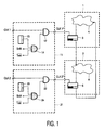
- FIG. 1 The schematic representation of Figure 1 shows in its right part some sections an otherwise not shown integrated circuit, so are a first Circuit element 1 and a second circuit element 2 is provided.
- first Circuit element 1 are otherwise not shown and only schematically indicated circuit parts 4 are provided.
- circuit part 3 is shown, which is clocked by means of a first clock signal (CLK 1 *).
- circuit element 2 To the circuit element 2 include there also not shown and only schematically indicated circuit parts 6. However, in this section is also a Circuit part 5 is provided, which is shown in detail and by means of a second Clock signal CLK 2 * is clocked.
- circuit parts 3 and 5 are such circuit parts, the zu testing integrated circuit, its operation by several clock signals and whose flank uncertainty is influenced.
- the exact phase behavior of the two clock signals CLK 1 * and CLK 2 * to each other the behavior of the circuit parts 3 and 5 influenced. It can be like this, for example be that the acquisition of the data from the circuit part 3 in the circuit part 5 of the exact phase behavior of the two clock signals CLK 1 * and CLK 2 * to each other depends.
- test software is based on the hardware circuit, which is indicated in Figure 1, preceded that in the integrated circuit, the individual Clock signals are switchable.
- a first switching logic 11 is provided which it allows to switch an original first clock signal CLK 1 as needed and from it to form the first clock signal CLK 1 *.
- an AND gate is provided, on the one hand the original Clock signal CLK 1 is supplied and in addition to a second input Output signal of an OR gate 14 is supplied.
- the OR gate 14 has three Inputs to which an output signal of a first flip-flop 13, a shift signal, in the figure is marked with shift, and an inverted test signal, which in the figure presented with test.
- the shift signal Shift is a signal which activates during testing will be pushed as long as new data in the integrated circuit or out to be read out.
- the inverted test signal Test then has low amplitude, when a test is taking place.
- the test signal has low amplitude 1. Further, the Shift signal Shift low amplitude 1, if no sliding of data in the integrated circuit or takes place from this. Thus hangs during this Operating times in testing the output of the OR gate from which State the flip-flop 13 has.
- the state of the flip-flop 13, depends on whether from the test software in the manner not shown in the figure before a 0 or a 1 was pushed into the flip-flop. This 0 or 1 determines via the OR gate 14, whose output signal reaches the second input of the AND gate 12, whether the original clock signal CLK 1 to the output of the AND gate or not. in the In this way, depending on whether the test software generates a 0 or a 1 was loaded into the flip-flop 13, the clock signal CLK 1 * turned on or off become.
- an AND gate 22 an OR gate 24 and a second flip-flop 23 are provided. These work in appropriate As in the first switching logic 11 and allow it in this way, the second Clock signal CLK 2 * controlled by the test software on or off.
- the cutout 31 shows circuit parts 34, which are not shown in detail. He includes but also a circuit part 33, the circuit part 3 of the actual hardware represented as a model according to FIG. In the section 32 of the software model is Furthermore, a circuit part 35 is provided which the real circuit part 5 of the circuit represented as a model according to FIG.
- the clock signal CLK 1 ' is applied to a switching input of a multiplexer 37 whose two other inputs on the one hand the signal from the circuit parts 34 and on the other a fed back output signal of the circuit part 33 is supplied.
- the multiplexer 37 serves, in a test operation, if necessary, the state of the circuit part 33, in which it For example, to be a flip-flop can hold, so that with this held state of the circuit part 33 in other circuit parts in possibly several passes tests can be performed.
- the circuit part 35 is associated with a multiplexer 39 whose Switching input a clock signal CLK 2 'is supplied, which the clock signal CLK 2 * in corresponds to the real circuit of Figure 1.
- the software model according to FIG. 2 is configured. It is an inverting one And link 53 provided, Which the clock signal CLK 1 'and an OR link the two clock signals CLK 2 'and CLK x' linked together.
- the Circuit part 39 can only be measured when the clock CLK 1 'or in the real circuit, the clock signal CLK 1 * is activated.
- the software logic according to FIG. 2 is but switched so that the X-generator 38 is already activated when one of the two other clock signals CLK 2 'or CLK x' is present. It is then in fact existing clock CLK 1 'is a logical 0 at the output of the AND link 53 appear, which activates the X-generator 38.
- the associated X-generator 40 then is activated if one of the other clocks CLK 1 'or CLK y' is active.
- circuit parts 33 and 35 can be without influence of the skew problem be measured only if the associated clock CLK 1 ' or CLK2 'is activated exclusively.
- This X signal signals a test software not shown in the figure invalid measurement result or one which is influenced by the skew problem.
- test software can test the real circuit in parallel with the Monitor the software model and constantly determine which test results are valid. This namely, those test results for which there is no X signal in the software model shows up.
- the procedure for testing can be, for example, the following:
- a circuit is first tested by activating all clock signals. It will be that Software model observed and evaluates the test software in this first round only the test results for those components for which there is no X signal in the software model shows up. In subsequent tests, those components must be used be measured again for the first run in the software model an X-signal showed up.
- the clocks can be individually deactivated one after another until No X signal appears for every component. This procedure can be individually for the made of various components. Thus, one of the the Operation of this component influencing clock signals are made until for the Component no longer X-signal occurs.
Landscapes
- Engineering & Computer Science (AREA)
- General Engineering & Computer Science (AREA)
- Physics & Mathematics (AREA)
- General Physics & Mathematics (AREA)
- Tests Of Electronic Circuits (AREA)
- Semiconductor Integrated Circuits (AREA)
Description
dass jedes der Taktsignale von einer in der Anordnung vorgesehenen Testsoftware in einem Testbetrieb einzeln ein- und ausschaltbar ist
dass in der Anordnung ein Softwaremodell des zu testenden Schaltkreises vorgesehen ist, in welchem für solche Schaltungsteile, deren Arbeitsweise von mehreren Taktsignalen und deren Flankenunsicherheiten beeinflusst wird, ein X-Generator vorgesehen ist, der dann aktiviert wird und ein X-Signal liefert, wenn beim Testen mehr als eines die Arbeitsweise des Schaltungsteils beeinflussendes Taktsignale aktiviert ist,
dass die Testsoftware beim Testen zunächst alle Taktsignale aktiviert und Testergebnisse für diejenigen Schaltungsteile auswertet, für die in dem Softwaremodell kein X-Signal erscheint,
und dass die Testsoftware für diejenigen Schaltungsteile, für die in dem Softwaremodell beim Testen mit allen Taktsignalen ein X-Signal erschien, mehrere Testdurchläufe vornimmt, bei denen nur jeweils einer oder mehrere der die Arbeitsweise des Schaltungsteils beeinflussenden Taktsignale aktiviert ist/sind und nur diejenigen Tests der Schaltungsteile des Schaltkreises auswertet, für die in dem Softwaremodell kein X-Signal erscheint.
Die erfindungsgemäße Anordnung zum Testen eines integrierten Schaltkreises setzt voraus, dass dieser so ausgelegt ist, dass jedes der Taktsignale, das in dem integrierten Schaltkreis verwendet wird bzw. auftaucht, durch eine extern in der Anordnung vorgesehene Testsoftware im Testbetrieb einzeln ein- und ausschaltbar ist. Es soll also möglich sein, mittels der Testsoftware je nach Bedarf die einzelnen Taktsignale ein- oder auszuschalten, wobei es auch möglich sein soll, ggf. mehrere Taktsignale gleichzeitig zu aktivieren.
Claims (3)
- Anordnung zum Testen eines integrierten Schaltkreises, welcher wenigstens zwei Schaltungsteile (1,2) aufweist, die im Normalbetrieb mit wenigstens zwei verschiedenen Taktsignalen arbeiten,
dadurch gekennzeichnet, dass der zu testende integrierte Schaltkreis so ausgelegt ist, dass jedes der Taktsignale von einer in der Anordnung vorgesehenen Testsoftware in einem Testbetrieb einzeln ein- und ausschaltbar ist,
dass in der Anordnung ein Softwaremodell des zu testenden Schaltkreises vorgesehen ist, in welchem für solche Schaltungsteile (33, 35), deren Arbeitsweise von mehreren Taktsignalen und deren Flankenunsicherheiten beeinflusst wird, ein X-Generator (38,40) vorgesehen ist, der dann aktiviert wird und ein X-Signal liefert, wenn beim Testen mehr als eines die Arbeitsweise des Schaltungsteils (33,35) beeinflussendes Taktsignale aktiviert ist,
dass die Testsoftware beim Testen zunächst alle Taktsignale aktiviert und Testergebnisse für diejenigen Schaltungsteile (3,5) auswertet, für die in dem Softwaremodell (33,35) kein X-Signal erscheint,
und dass die Testsoftware für diejenigen Schaltungsteile (3,5), für die in dem Softwaremodell (33,35) beim Testen mit allen Taktsignalen ein X-Signal erschien, mehrere Testdurchläufe vornimmt, bei denen nur jeweils einer oder mehrere der die Arbeitsweise des Schaltungsteils (3,5) beeinflusenden Taktsignale aktiviert ist/sind und nur diejenigen Tests der Schaltungsteile (3,5) des Schaltkreises auswertet, für die in dem Softwaremodell (33,35) kein X-Signal erscheint. - Anordnung nach Anspruch 1,
dadurch gekennzeichnet, dass in dem zu testenden Schaltkreis für alle Schaltungsteile (3,5), die selbst mit einem zugeordneten Takt arbeiten und deren Arbeitsweise auch von anderen Taktsignalen beeinflusst wird, jeweils ein von der Testsoftware ladbares Flip-Flop (13,23) vorgesehen ist, dessen Ausgangssignal auf ein Oder-Gatter (14,24) geführt ist, dessen weiteren Eingängen ein Shift-Signal, das während eines Schiebevorgangs, in dem neue Daten in oder aus dem Schaltungselement (3,5) geschoben werden, High-Pegel hat, sowie ein invertiertes Testsignal, das während des Testens Low-Pegel hat, zugeführt werden, und dass das Ausgangssignal des Oder-Gatters (14,24) auf einen Eingang eines Und-Gatters (12,22) geführt ist, dessen anderem Eingang das zugeordnete Taktsignal des jeweiligen Schaltungsteils (3,5) zugeführt wird und dessen Ausgangssignal dem Schaltungsteil (3,5) als Takt zugeführt wird. - Anordnung nach Anspruch 1,
dadurch gekennzeichnet, dass die Testsoftware für diejenigen Schaltungselemente (3,5), für die in dem Softwaremodell (33,35) beim Testen mit allen Taktsignalen ein X-Signal erschien, zunächst Testdurchläufe vornimmt, bei denen nur jeweils einer die Arbeitsweise des Schaltungsteils (3,5) beeinflussenden Taktsignale deaktiviert ist, und dass die Testsoftware, sollte in diesem Test auch ein X-Signal für bestimmte Schaltungsteile (33,35) erscheinen, die Anzahl der deaktivierten Taktsignale soweit gesteigert bis in dem Softwaremodell für die Schaltungsteile (33,35) kein X-Signal mehr erscheint und eine Auswertung der Testergebnisse der betreffenden Schaltungsteile (3,5) erfolgen kann.
Applications Claiming Priority (2)
| Application Number | Priority Date | Filing Date | Title |
|---|---|---|---|
| DE10039001 | 2000-08-10 | ||
| DE10039001A DE10039001A1 (de) | 2000-08-10 | 2000-08-10 | Anordnung zum Testen eines integrierten Schaltkreises |
Publications (3)
| Publication Number | Publication Date |
|---|---|
| EP1179737A2 EP1179737A2 (de) | 2002-02-13 |
| EP1179737A3 EP1179737A3 (de) | 2003-10-15 |
| EP1179737B1 true EP1179737B1 (de) | 2005-03-09 |
Family
ID=7651937
Family Applications (1)
| Application Number | Title | Priority Date | Filing Date |
|---|---|---|---|
| EP01000351A Expired - Lifetime EP1179737B1 (de) | 2000-08-10 | 2001-08-07 | Anordnung zum Testen eines integrierten Schaltkreises |
Country Status (4)
| Country | Link |
|---|---|
| US (1) | US6789219B2 (de) |
| EP (1) | EP1179737B1 (de) |
| JP (1) | JP2002116240A (de) |
| DE (2) | DE10039001A1 (de) |
Families Citing this family (7)
| Publication number | Priority date | Publication date | Assignee | Title |
|---|---|---|---|---|
| US7198197B2 (en) * | 2002-11-05 | 2007-04-03 | Rambus, Inc. | Method and apparatus for data acquisition |
| WO2005071426A1 (en) * | 2004-01-19 | 2005-08-04 | Koninklijke Philips Electronics N.V. | Testing of circuits with multiple clock domains |
| US8036873B2 (en) * | 2005-02-28 | 2011-10-11 | Synopsys, Inc. | Efficient clock models and their use in simulation |
| JP4845543B2 (ja) * | 2006-03-15 | 2011-12-28 | 富士通セミコンダクター株式会社 | 遅延故障試験回路 |
| DE102006024507B4 (de) | 2006-05-23 | 2017-06-01 | Infineon Technologies Ag | Integrierte Schaltung und Verfahren zum Erkennen von Laufzeitfehlern in integrierten Schaltungen |
| US8768679B2 (en) | 2010-09-30 | 2014-07-01 | International Business Machines Corporation | System and method for efficient modeling of NPskew effects on static timing tests |
| CN108226743B (zh) * | 2016-12-22 | 2020-04-24 | 深圳市中兴微电子技术有限公司 | 一种测试向量的生成方法及装置 |
Family Cites Families (9)
| Publication number | Priority date | Publication date | Assignee | Title |
|---|---|---|---|---|
| US4791356A (en) * | 1986-09-19 | 1988-12-13 | Zehntel Incorporation | In-circuit testing system |
| DE69115338T2 (de) * | 1990-04-20 | 1996-05-09 | Texas Instruments Inc | Abtasttestschaltung zur Verwendung mit Mehrfrequenzschaltungen |
| US5349587A (en) | 1992-03-26 | 1994-09-20 | Northern Telecom Limited | Multiple clock rate test apparatus for testing digital systems |
| US5838894A (en) * | 1992-12-17 | 1998-11-17 | Tandem Computers Incorporated | Logical, fail-functional, dual central processor units formed from three processor units |
| EP0642083A1 (de) * | 1993-09-04 | 1995-03-08 | International Business Machines Corporation | Prüfschaltkreis und Verfahren zum Prüfen von Chipverbindungen |
| US5526286A (en) * | 1994-02-16 | 1996-06-11 | Tektronix, Inc. | Oversampled logic analyzer |
| US5630102A (en) * | 1994-12-19 | 1997-05-13 | Intel Corporation | In-circuit-emulation event management system |
| EP0886784B1 (de) * | 1996-12-13 | 2005-04-06 | Koninklijke Philips Electronics N.V. | Integrierte schaltung mit einer ersten und zweiten taktdomäne und prüfvorrichtung für eine solche schaltung |
| US6029261A (en) * | 1997-10-14 | 2000-02-22 | International Business Machines Corporation | Test circuit and system for interconnect testing of high-level packages |
-
2000
- 2000-08-10 DE DE10039001A patent/DE10039001A1/de not_active Withdrawn
-
2001
- 2001-08-07 EP EP01000351A patent/EP1179737B1/de not_active Expired - Lifetime
- 2001-08-07 US US09/923,614 patent/US6789219B2/en not_active Expired - Fee Related
- 2001-08-07 DE DE50105516T patent/DE50105516D1/de not_active Expired - Lifetime
- 2001-08-09 JP JP2001242561A patent/JP2002116240A/ja not_active Withdrawn
Also Published As
| Publication number | Publication date |
|---|---|
| DE10039001A1 (de) | 2002-02-21 |
| DE50105516D1 (de) | 2005-04-14 |
| EP1179737A3 (de) | 2003-10-15 |
| EP1179737A2 (de) | 2002-02-13 |
| US20020069385A1 (en) | 2002-06-06 |
| US6789219B2 (en) | 2004-09-07 |
| JP2002116240A (ja) | 2002-04-19 |
Similar Documents
| Publication | Publication Date | Title |
|---|---|---|
| DE2311034C2 (de) | Verfahren zum Prüfen eines integrierte logische Verknüpfungs- und Speicherglieder enthaltenden Halbleiterchips | |
| DE2729053C2 (de) | Prüfverfahren für eine monolithisch integrierte stufenempfindliche, einseitig verzögerungsabhängige logische Einheit | |
| DE3882266T2 (de) | Abfrageprüfgerät für digitale Systeme mit dynamischem Direktzugriffspeicher. | |
| DE69126848T2 (de) | Integrierte Halbleiterschaltung | |
| DE3702408C2 (de) | ||
| DE2346617A1 (de) | Verfahren zur pruefung der laufzeitverzoegerung einer funktionalen logischen einheit | |
| DE2349324A1 (de) | Verfahren und vorrichtung zum pruefen funktioneller logischer schaltungen | |
| DE69019555T2 (de) | Technik für die serielle Prüfung eingebauter Speicher. | |
| EP0144078A2 (de) | Verfahren und Anordnung zum Prüfen einer Schaltung nach der Abfragepfad-Technik | |
| DE10120080B4 (de) | Ereignisgestütztes Prüfsystem mit einer Einrichtung zur Erzeugung von Prüfabschluß-Mehrfachsignalen | |
| DE19536226C2 (de) | Testbare Schaltungsanordnung mit mehreren identischen Schaltungsblöcken | |
| DE102021128331B3 (de) | Integrierte schaltung, testanordnung und verfahren zum testen einer integrierten schaltung | |
| DE69017169T2 (de) | Testen integrierter Schaltungen unter Verwendung von Taktgeberstössen. | |
| DE3587620T2 (de) | Logikanalysator. | |
| EP1217630A2 (de) | Verfahren zur Prüfung von einer integrierten Schaltung | |
| DE69522663T2 (de) | Bypass-regelung für abtastprüfung mit selbsttätiger rückstellung | |
| EP1179737A2 (de) | Anordnung zum Testen eines integrierten Schaltkreises | |
| DE69027545T2 (de) | Vorrichtung und Verfahren zum Frequenzwechsel | |
| DE3486064T2 (de) | Logische schaltung mit eingebauter selbsttestfunktion. | |
| DE102008003450B4 (de) | Digitalschaltungen und Verfahren zum Testen einer Digitalschaltung | |
| DE69430304T2 (de) | Anordnung zum testen von verbindungen mit pulling-widerständen | |
| DE19901460C1 (de) | Integrierte Halbleiterschaltung und Verfahren zur Überprüfung des Übertragungsverhaltens von Pad-Zellen | |
| DE602005005084T2 (de) | Testfähige integrierte schaltung | |
| DE3839289C1 (en) | Circuit for the operation of an integrated circuit of which it is a component, optionally in a test operation mode or a functional operation mode | |
| DE10110777A1 (de) | Anordnung und Verfahren zum Testen von integrierten Schaltkreisen |
Legal Events
| Date | Code | Title | Description |
|---|---|---|---|
| PUAI | Public reference made under article 153(3) epc to a published international application that has entered the european phase |
Free format text: ORIGINAL CODE: 0009012 |
|
| AK | Designated contracting states |
Kind code of ref document: A2 Designated state(s): AT BE CH CY DE DK ES FI FR GB GR IE IT LI LU MC NL PT SE TR |
|
| AX | Request for extension of the european patent |
Free format text: AL;LT;LV;MK;RO;SI |
|
| RAP1 | Party data changed (applicant data changed or rights of an application transferred) |
Owner name: KONINKLIJKE PHILIPS ELECTRONICS N.V. Owner name: PHILIPS CORPORATE INTELLECTUAL PROPERTY GMBH |
|
| RAP1 | Party data changed (applicant data changed or rights of an application transferred) |
Owner name: PHILIPS INTELLECTUAL PROPERTY & STANDARDS GMBH Owner name: KONINKLIJKE PHILIPS ELECTRONICS N.V. |
|
| PUAL | Search report despatched |
Free format text: ORIGINAL CODE: 0009013 |
|
| AK | Designated contracting states |
Kind code of ref document: A3 Designated state(s): AT BE CH CY DE DK ES FI FR GB GR IE IT LI LU MC NL PT SE TR |
|
| AX | Request for extension of the european patent |
Extension state: AL LT LV MK RO SI |
|
| GRAP | Despatch of communication of intention to grant a patent |
Free format text: ORIGINAL CODE: EPIDOSNIGR1 |
|
| 17P | Request for examination filed |
Effective date: 20040415 |
|
| AKX | Designation fees paid |
Designated state(s): DE FR GB |
|
| GRAS | Grant fee paid |
Free format text: ORIGINAL CODE: EPIDOSNIGR3 |
|
| GRAA | (expected) grant |
Free format text: ORIGINAL CODE: 0009210 |
|
| AK | Designated contracting states |
Kind code of ref document: B1 Designated state(s): DE FR GB |
|
| REG | Reference to a national code |
Ref country code: GB Ref legal event code: FG4D Free format text: NOT ENGLISH |
|
| REG | Reference to a national code |
Ref country code: IE Ref legal event code: FG4D Free format text: GERMAN |
|
| REF | Corresponds to: |
Ref document number: 50105516 Country of ref document: DE Date of ref document: 20050414 Kind code of ref document: P |
|
| GBT | Gb: translation of ep patent filed (gb section 77(6)(a)/1977) |
Effective date: 20050525 |
|
| PLBE | No opposition filed within time limit |
Free format text: ORIGINAL CODE: 0009261 |
|
| STAA | Information on the status of an ep patent application or granted ep patent |
Free format text: STATUS: NO OPPOSITION FILED WITHIN TIME LIMIT |
|
| ET | Fr: translation filed | ||
| 26N | No opposition filed |
Effective date: 20051212 |
|
| REG | Reference to a national code |
Ref country code: GB Ref legal event code: 732E |
|
| REG | Reference to a national code |
Ref country code: FR Ref legal event code: TP |
|
| PGFP | Annual fee paid to national office [announced via postgrant information from national office to epo] |
Ref country code: DE Payment date: 20090730 Year of fee payment: 9 |
|
| PGFP | Annual fee paid to national office [announced via postgrant information from national office to epo] |
Ref country code: FR Payment date: 20100824 Year of fee payment: 10 |
|
| REG | Reference to a national code |
Ref country code: DE Ref legal event code: R119 Ref document number: 50105516 Country of ref document: DE Effective date: 20110301 |
|
| PG25 | Lapsed in a contracting state [announced via postgrant information from national office to epo] |
Ref country code: DE Free format text: LAPSE BECAUSE OF NON-PAYMENT OF DUE FEES Effective date: 20110301 |
|
| PGFP | Annual fee paid to national office [announced via postgrant information from national office to epo] |
Ref country code: GB Payment date: 20110728 Year of fee payment: 11 |
|
| REG | Reference to a national code |
Ref country code: FR Ref legal event code: ST Effective date: 20120430 |
|
| PG25 | Lapsed in a contracting state [announced via postgrant information from national office to epo] |
Ref country code: FR Free format text: LAPSE BECAUSE OF NON-PAYMENT OF DUE FEES Effective date: 20110831 |
|
| GBPC | Gb: european patent ceased through non-payment of renewal fee |
Effective date: 20120807 |
|
| PG25 | Lapsed in a contracting state [announced via postgrant information from national office to epo] |
Ref country code: GB Free format text: LAPSE BECAUSE OF NON-PAYMENT OF DUE FEES Effective date: 20120807 |