EP1178024A2 - Reduction-resistant dielectric ceramic compact and laminated ceramic capacitor - Google Patents
Reduction-resistant dielectric ceramic compact and laminated ceramic capacitor Download PDFInfo
- Publication number
- EP1178024A2 EP1178024A2 EP01116386A EP01116386A EP1178024A2 EP 1178024 A2 EP1178024 A2 EP 1178024A2 EP 01116386 A EP01116386 A EP 01116386A EP 01116386 A EP01116386 A EP 01116386A EP 1178024 A2 EP1178024 A2 EP 1178024A2
- Authority
- EP
- European Patent Office
- Prior art keywords
- dielectric ceramic
- reduction
- compound containing
- resistant dielectric
- primary component
- Prior art date
- Legal status (The legal status is an assumption and is not a legal conclusion. Google has not performed a legal analysis and makes no representation as to the accuracy of the status listed.)
- Withdrawn
Links
- 239000000919 ceramic Substances 0.000 title claims abstract description 129
- 239000003985 ceramic capacitor Substances 0.000 title claims abstract description 72
- PXHVJJICTQNCMI-UHFFFAOYSA-N Nickel Chemical compound [Ni] PXHVJJICTQNCMI-UHFFFAOYSA-N 0.000 claims abstract description 54
- 150000001875 compounds Chemical group 0.000 claims abstract description 54
- 238000005245 sintering Methods 0.000 claims abstract description 41
- 229910002113 barium titanate Inorganic materials 0.000 claims abstract description 39
- JRPBQTZRNDNNOP-UHFFFAOYSA-N barium titanate Chemical compound [Ba+2].[Ba+2].[O-][Ti]([O-])([O-])[O-] JRPBQTZRNDNNOP-UHFFFAOYSA-N 0.000 claims abstract description 38
- 239000003795 chemical substances by application Substances 0.000 claims abstract description 32
- 229910052759 nickel Inorganic materials 0.000 claims abstract description 29
- 239000006104 solid solution Substances 0.000 claims abstract description 27
- 238000002441 X-ray diffraction Methods 0.000 claims abstract description 10
- GWEVSGVZZGPLCZ-UHFFFAOYSA-N titanium dioxide Inorganic materials O=[Ti]=O GWEVSGVZZGPLCZ-UHFFFAOYSA-N 0.000 claims description 41
- 229910052735 hafnium Inorganic materials 0.000 claims description 32
- 238000007747 plating Methods 0.000 claims description 19
- 229910052710 silicon Inorganic materials 0.000 claims description 14
- 239000010703 silicon Substances 0.000 claims description 14
- 239000011521 glass Substances 0.000 claims description 13
- RYGMFSIKBFXOCR-UHFFFAOYSA-N Copper Chemical compound [Cu] RYGMFSIKBFXOCR-UHFFFAOYSA-N 0.000 claims description 11
- 229910052802 copper Inorganic materials 0.000 claims description 11
- 239000010949 copper Substances 0.000 claims description 11
- 229910052717 sulfur Inorganic materials 0.000 claims description 11
- ZOXJGFHDIHLPTG-UHFFFAOYSA-N Boron Chemical compound [B] ZOXJGFHDIHLPTG-UHFFFAOYSA-N 0.000 claims description 10
- 229910052796 boron Inorganic materials 0.000 claims description 10
- 229910000990 Ni alloy Inorganic materials 0.000 claims description 8
- VYPSYNLAJGMNEJ-UHFFFAOYSA-N Silicium dioxide Chemical compound O=[Si]=O VYPSYNLAJGMNEJ-UHFFFAOYSA-N 0.000 claims description 8
- 229910052782 aluminium Inorganic materials 0.000 claims description 8
- 229910000881 Cu alloy Inorganic materials 0.000 claims description 7
- 229910052788 barium Inorganic materials 0.000 claims description 7
- 229910052791 calcium Inorganic materials 0.000 claims description 7
- 229910052742 iron Inorganic materials 0.000 claims description 7
- 229910052712 strontium Inorganic materials 0.000 claims description 7
- 229910052725 zinc Inorganic materials 0.000 claims description 6
- 229910052749 magnesium Inorganic materials 0.000 claims description 5
- 229910052751 metal Inorganic materials 0.000 claims description 5
- 239000002184 metal Substances 0.000 claims description 5
- 229910052720 vanadium Inorganic materials 0.000 claims description 5
- 229910052727 yttrium Inorganic materials 0.000 claims description 5
- 229910052684 Cerium Inorganic materials 0.000 claims description 4
- 229910052692 Dysprosium Inorganic materials 0.000 claims description 4
- 229910052691 Erbium Inorganic materials 0.000 claims description 4
- 229910052693 Europium Inorganic materials 0.000 claims description 4
- 229910052688 Gadolinium Inorganic materials 0.000 claims description 4
- 229910052689 Holmium Inorganic materials 0.000 claims description 4
- 229910052779 Neodymium Inorganic materials 0.000 claims description 4
- 229910052777 Praseodymium Inorganic materials 0.000 claims description 4
- 229910052772 Samarium Inorganic materials 0.000 claims description 4
- 229910052771 Terbium Inorganic materials 0.000 claims description 4
- 229910052775 Thulium Inorganic materials 0.000 claims description 4
- 229910052769 Ytterbium Inorganic materials 0.000 claims description 4
- 229910052804 chromium Inorganic materials 0.000 claims description 4
- 229910052746 lanthanum Inorganic materials 0.000 claims description 4
- 229910052748 manganese Inorganic materials 0.000 claims description 4
- 229910052750 molybdenum Inorganic materials 0.000 claims description 4
- 229910052758 niobium Inorganic materials 0.000 claims description 4
- 229910052814 silicon oxide Inorganic materials 0.000 claims description 4
- 229910052715 tantalum Inorganic materials 0.000 claims description 4
- 229910052721 tungsten Inorganic materials 0.000 claims description 4
- 238000011068 loading method Methods 0.000 abstract description 36
- 239000007772 electrode material Substances 0.000 abstract description 15
- 230000020169 heat generation Effects 0.000 abstract description 15
- 230000005684 electric field Effects 0.000 abstract description 4
- 239000007858 starting material Substances 0.000 description 33
- 239000000203 mixture Substances 0.000 description 20
- 239000010953 base metal Substances 0.000 description 16
- 230000007547 defect Effects 0.000 description 15
- 238000010304 firing Methods 0.000 description 13
- 239000000463 material Substances 0.000 description 13
- AYJRCSIUFZENHW-UHFFFAOYSA-L barium carbonate Chemical compound [Ba+2].[O-]C([O-])=O AYJRCSIUFZENHW-UHFFFAOYSA-L 0.000 description 12
- 230000003247 decreasing effect Effects 0.000 description 12
- 239000012071 phase Substances 0.000 description 11
- VTYYLEPIZMXCLO-UHFFFAOYSA-L Calcium carbonate Chemical compound [Ca+2].[O-]C([O-])=O VTYYLEPIZMXCLO-UHFFFAOYSA-L 0.000 description 10
- 230000003068 static effect Effects 0.000 description 10
- 230000007704 transition Effects 0.000 description 10
- PNEYBMLMFCGWSK-UHFFFAOYSA-N aluminium oxide Inorganic materials [O-2].[O-2].[O-2].[Al+3].[Al+3] PNEYBMLMFCGWSK-UHFFFAOYSA-N 0.000 description 9
- 229910052593 corundum Inorganic materials 0.000 description 9
- 238000000034 method Methods 0.000 description 9
- 229910001845 yogo sapphire Inorganic materials 0.000 description 9
- 229910052726 zirconium Inorganic materials 0.000 description 9
- KKCBUQHMOMHUOY-UHFFFAOYSA-N Na2O Inorganic materials [O-2].[Na+].[Na+] KKCBUQHMOMHUOY-UHFFFAOYSA-N 0.000 description 6
- 239000012298 atmosphere Substances 0.000 description 6
- QDOXWKRWXJOMAK-UHFFFAOYSA-N dichromium trioxide Chemical compound O=[Cr]O[Cr]=O QDOXWKRWXJOMAK-UHFFFAOYSA-N 0.000 description 6
- GNTDGMZSJNCJKK-UHFFFAOYSA-N divanadium pentaoxide Chemical compound O=[V](=O)O[V](=O)=O GNTDGMZSJNCJKK-UHFFFAOYSA-N 0.000 description 6
- JEIPFZHSYJVQDO-UHFFFAOYSA-N iron(III) oxide Inorganic materials O=[Fe]O[Fe]=O JEIPFZHSYJVQDO-UHFFFAOYSA-N 0.000 description 6
- JKQOBWVOAYFWKG-UHFFFAOYSA-N molybdenum trioxide Chemical compound O=[Mo](=O)=O JKQOBWVOAYFWKG-UHFFFAOYSA-N 0.000 description 6
- ZKATWMILCYLAPD-UHFFFAOYSA-N niobium pentoxide Chemical compound O=[Nb](=O)O[Nb](=O)=O ZKATWMILCYLAPD-UHFFFAOYSA-N 0.000 description 6
- DLYUQMMRRRQYAE-UHFFFAOYSA-N tetraphosphorus decaoxide Chemical compound O1P(O2)(=O)OP3(=O)OP1(=O)OP2(=O)O3 DLYUQMMRRRQYAE-UHFFFAOYSA-N 0.000 description 6
- -1 Tb4O7 Inorganic materials 0.000 description 5
- QVGXLLKOCUKJST-UHFFFAOYSA-N atomic oxygen Chemical compound [O] QVGXLLKOCUKJST-UHFFFAOYSA-N 0.000 description 5
- 229910000019 calcium carbonate Inorganic materials 0.000 description 5
- RSEIMSPAXMNYFJ-UHFFFAOYSA-N europium(III) oxide Inorganic materials O=[Eu]O[Eu]=O RSEIMSPAXMNYFJ-UHFFFAOYSA-N 0.000 description 5
- CMIHHWBVHJVIGI-UHFFFAOYSA-N gadolinium(III) oxide Inorganic materials [O-2].[O-2].[O-2].[Gd+3].[Gd+3] CMIHHWBVHJVIGI-UHFFFAOYSA-N 0.000 description 5
- CPLXHLVBOLITMK-UHFFFAOYSA-N magnesium oxide Inorganic materials [Mg]=O CPLXHLVBOLITMK-UHFFFAOYSA-N 0.000 description 5
- VASIZKWUTCETSD-UHFFFAOYSA-N manganese(II) oxide Inorganic materials [Mn]=O VASIZKWUTCETSD-UHFFFAOYSA-N 0.000 description 5
- GNRSAWUEBMWBQH-UHFFFAOYSA-N nickel(II) oxide Inorganic materials [Ni]=O GNRSAWUEBMWBQH-UHFFFAOYSA-N 0.000 description 5
- 229910052760 oxygen Inorganic materials 0.000 description 5
- 239000001301 oxygen Substances 0.000 description 5
- 230000036961 partial effect Effects 0.000 description 5
- LEDMRZGFZIAGGB-UHFFFAOYSA-L strontium carbonate Chemical compound [Sr+2].[O-]C([O-])=O LEDMRZGFZIAGGB-UHFFFAOYSA-L 0.000 description 5
- 229910000018 strontium carbonate Inorganic materials 0.000 description 5
- KDLHZDBZIXYQEI-UHFFFAOYSA-N Palladium Chemical compound [Pd] KDLHZDBZIXYQEI-UHFFFAOYSA-N 0.000 description 4
- 239000003990 capacitor Substances 0.000 description 4
- NLQFUUYNQFMIJW-UHFFFAOYSA-N dysprosium(III) oxide Inorganic materials O=[Dy]O[Dy]=O NLQFUUYNQFMIJW-UHFFFAOYSA-N 0.000 description 4
- 239000012535 impurity Substances 0.000 description 4
- 229910003443 lutetium oxide Inorganic materials 0.000 description 4
- 238000004519 manufacturing process Methods 0.000 description 4
- BASFCYQUMIYNBI-UHFFFAOYSA-N platinum Chemical compound [Pt] BASFCYQUMIYNBI-UHFFFAOYSA-N 0.000 description 4
- 239000002002 slurry Substances 0.000 description 4
- 229910000679 solder Inorganic materials 0.000 description 4
- 239000000126 substance Substances 0.000 description 4
- 229910002976 CaZrO3 Inorganic materials 0.000 description 3
- MUBZPKHOEPUJKR-UHFFFAOYSA-N Oxalic acid Chemical compound OC(=O)C(O)=O MUBZPKHOEPUJKR-UHFFFAOYSA-N 0.000 description 3
- 229910002637 Pr6O11 Inorganic materials 0.000 description 3
- 229910021523 barium zirconate Inorganic materials 0.000 description 3
- 239000011230 binding agent Substances 0.000 description 3
- 238000007906 compression Methods 0.000 description 3
- JYTUFVYWTIKZGR-UHFFFAOYSA-N holmium oxide Inorganic materials [O][Ho]O[Ho][O] JYTUFVYWTIKZGR-UHFFFAOYSA-N 0.000 description 3
- MRELNEQAGSRDBK-UHFFFAOYSA-N lanthanum oxide Inorganic materials [O-2].[O-2].[O-2].[La+3].[La+3] MRELNEQAGSRDBK-UHFFFAOYSA-N 0.000 description 3
- KTUFCUMIWABKDW-UHFFFAOYSA-N oxo(oxolanthaniooxy)lanthanum Chemical compound O=[La]O[La]=O KTUFCUMIWABKDW-UHFFFAOYSA-N 0.000 description 3
- FKTOIHSPIPYAPE-UHFFFAOYSA-N samarium(III) oxide Inorganic materials [O-2].[O-2].[O-2].[Sm+3].[Sm+3] FKTOIHSPIPYAPE-UHFFFAOYSA-N 0.000 description 3
- 239000000243 solution Substances 0.000 description 3
- 229910014031 strontium zirconium oxide Inorganic materials 0.000 description 3
- PBCFLUZVCVVTBY-UHFFFAOYSA-N tantalum pentoxide Inorganic materials O=[Ta](=O)O[Ta](=O)=O PBCFLUZVCVVTBY-UHFFFAOYSA-N 0.000 description 3
- ZIKATJAYWZUJPY-UHFFFAOYSA-N thulium (III) oxide Inorganic materials [O-2].[O-2].[O-2].[Tm+3].[Tm+3] ZIKATJAYWZUJPY-UHFFFAOYSA-N 0.000 description 3
- ZNOKGRXACCSDPY-UHFFFAOYSA-N tungsten(VI) oxide Inorganic materials O=[W](=O)=O ZNOKGRXACCSDPY-UHFFFAOYSA-N 0.000 description 3
- FIXNOXLJNSSSLJ-UHFFFAOYSA-N ytterbium(III) oxide Inorganic materials O=[Yb]O[Yb]=O FIXNOXLJNSSSLJ-UHFFFAOYSA-N 0.000 description 3
- RUDFQVOCFDJEEF-UHFFFAOYSA-N yttrium(III) oxide Inorganic materials [O-2].[O-2].[O-2].[Y+3].[Y+3] RUDFQVOCFDJEEF-UHFFFAOYSA-N 0.000 description 3
- LFQSCWFLJHTTHZ-UHFFFAOYSA-N Ethanol Chemical compound CCO LFQSCWFLJHTTHZ-UHFFFAOYSA-N 0.000 description 2
- 229910052765 Lutetium Inorganic materials 0.000 description 2
- 229910001252 Pd alloy Inorganic materials 0.000 description 2
- ATJFFYVFTNAWJD-UHFFFAOYSA-N Tin Chemical compound [Sn] ATJFFYVFTNAWJD-UHFFFAOYSA-N 0.000 description 2
- 150000004703 alkoxides Chemical class 0.000 description 2
- DSAJWYNOEDNPEQ-UHFFFAOYSA-N barium atom Chemical compound [Ba] DSAJWYNOEDNPEQ-UHFFFAOYSA-N 0.000 description 2
- 230000015556 catabolic process Effects 0.000 description 2
- CETPSERCERDGAM-UHFFFAOYSA-N ceric oxide Chemical compound O=[Ce]=O CETPSERCERDGAM-UHFFFAOYSA-N 0.000 description 2
- 229910000422 cerium(IV) oxide Inorganic materials 0.000 description 2
- 229910052681 coesite Inorganic materials 0.000 description 2
- 230000006835 compression Effects 0.000 description 2
- 229910052906 cristobalite Inorganic materials 0.000 description 2
- 239000003989 dielectric material Substances 0.000 description 2
- 230000007935 neutral effect Effects 0.000 description 2
- 239000012299 nitrogen atmosphere Substances 0.000 description 2
- 230000001590 oxidative effect Effects 0.000 description 2
- 229910052763 palladium Inorganic materials 0.000 description 2
- SWELZOZIOHGSPA-UHFFFAOYSA-N palladium silver Chemical compound [Pd].[Ag] SWELZOZIOHGSPA-UHFFFAOYSA-N 0.000 description 2
- 229910052697 platinum Inorganic materials 0.000 description 2
- 239000000843 powder Substances 0.000 description 2
- 239000012254 powdered material Substances 0.000 description 2
- 239000012255 powdered metal Substances 0.000 description 2
- 238000010298 pulverizing process Methods 0.000 description 2
- HYXGAEYDKFCVMU-UHFFFAOYSA-N scandium(III) oxide Inorganic materials O=[Sc]O[Sc]=O HYXGAEYDKFCVMU-UHFFFAOYSA-N 0.000 description 2
- 239000004065 semiconductor Substances 0.000 description 2
- 239000000377 silicon dioxide Substances 0.000 description 2
- 229910052682 stishovite Inorganic materials 0.000 description 2
- 229910052905 tridymite Inorganic materials 0.000 description 2
- 238000012935 Averaging Methods 0.000 description 1
- 229910021586 Nickel(II) chloride Inorganic materials 0.000 description 1
- 238000003991 Rietveld refinement Methods 0.000 description 1
- 229910010252 TiO3 Inorganic materials 0.000 description 1
- 230000002411 adverse Effects 0.000 description 1
- KGBXLFKZBHKPEV-UHFFFAOYSA-N boric acid Chemical compound OB(O)O KGBXLFKZBHKPEV-UHFFFAOYSA-N 0.000 description 1
- 239000004327 boric acid Substances 0.000 description 1
- 238000001354 calcination Methods 0.000 description 1
- 150000005323 carbonate salts Chemical class 0.000 description 1
- 239000011248 coating agent Substances 0.000 description 1
- 238000000576 coating method Methods 0.000 description 1
- 239000008119 colloidal silica Substances 0.000 description 1
- 239000013078 crystal Substances 0.000 description 1
- 238000000151 deposition Methods 0.000 description 1
- 238000007606 doctor blade method Methods 0.000 description 1
- 238000001035 drying Methods 0.000 description 1
- VQCBHWLJZDBHOS-UHFFFAOYSA-N erbium(III) oxide Inorganic materials O=[Er]O[Er]=O VQCBHWLJZDBHOS-UHFFFAOYSA-N 0.000 description 1
- 238000011156 evaluation Methods 0.000 description 1
- 230000001747 exhibiting effect Effects 0.000 description 1
- 239000007789 gas Substances 0.000 description 1
- PCHJSUWPFVWCPO-UHFFFAOYSA-N gold Chemical compound [Au] PCHJSUWPFVWCPO-UHFFFAOYSA-N 0.000 description 1
- 229910052737 gold Inorganic materials 0.000 description 1
- 239000010931 gold Substances 0.000 description 1
- 150000004679 hydroxides Chemical class 0.000 description 1
- 230000010354 integration Effects 0.000 description 1
- 238000010030 laminating Methods 0.000 description 1
- 230000007257 malfunction Effects 0.000 description 1
- 150000002736 metal compounds Chemical class 0.000 description 1
- 238000002156 mixing Methods 0.000 description 1
- PLDDOISOJJCEMH-UHFFFAOYSA-N neodymium oxide Inorganic materials [O-2].[O-2].[O-2].[Nd+3].[Nd+3] PLDDOISOJJCEMH-UHFFFAOYSA-N 0.000 description 1
- QMMRZOWCJAIUJA-UHFFFAOYSA-L nickel dichloride Chemical compound Cl[Ni]Cl QMMRZOWCJAIUJA-UHFFFAOYSA-L 0.000 description 1
- LGQLOGILCSXPEA-UHFFFAOYSA-L nickel sulfate Chemical compound [Ni+2].[O-]S([O-])(=O)=O LGQLOGILCSXPEA-UHFFFAOYSA-L 0.000 description 1
- 229910000363 nickel(II) sulfate Inorganic materials 0.000 description 1
- 229910000510 noble metal Inorganic materials 0.000 description 1
- 239000003960 organic solvent Substances 0.000 description 1
- 235000006408 oxalic acid Nutrition 0.000 description 1
- 230000003647 oxidation Effects 0.000 description 1
- 238000007254 oxidation reaction Methods 0.000 description 1
- 239000002245 particle Substances 0.000 description 1
- 230000002093 peripheral effect Effects 0.000 description 1
- 229920002037 poly(vinyl butyral) polymer Polymers 0.000 description 1
- 238000007639 printing Methods 0.000 description 1
- 238000010791 quenching Methods 0.000 description 1
- 230000000171 quenching effect Effects 0.000 description 1
- 229910052761 rare earth metal Inorganic materials 0.000 description 1
- 230000002829 reductive effect Effects 0.000 description 1
- 229910052706 scandium Inorganic materials 0.000 description 1
- 238000007650 screen-printing Methods 0.000 description 1
- 229910052709 silver Inorganic materials 0.000 description 1
- 239000004332 silver Substances 0.000 description 1
- 238000010532 solid phase synthesis reaction Methods 0.000 description 1
- 238000010189 synthetic method Methods 0.000 description 1
- OGIDPMRJRNCKJF-UHFFFAOYSA-N titanium oxide Inorganic materials [Ti]=O OGIDPMRJRNCKJF-UHFFFAOYSA-N 0.000 description 1
- 238000005303 weighing Methods 0.000 description 1
- XLOMVQKBTHCTTD-UHFFFAOYSA-N zinc oxide Inorganic materials [Zn]=O XLOMVQKBTHCTTD-UHFFFAOYSA-N 0.000 description 1
Images

Classifications
-
- H—ELECTRICITY
- H01—ELECTRIC ELEMENTS
- H01G—CAPACITORS; CAPACITORS, RECTIFIERS, DETECTORS, SWITCHING DEVICES, LIGHT-SENSITIVE OR TEMPERATURE-SENSITIVE DEVICES OF THE ELECTROLYTIC TYPE
- H01G4/00—Fixed capacitors; Processes of their manufacture
- H01G4/30—Stacked capacitors
-
- H—ELECTRICITY
- H01—ELECTRIC ELEMENTS
- H01G—CAPACITORS; CAPACITORS, RECTIFIERS, DETECTORS, SWITCHING DEVICES, LIGHT-SENSITIVE OR TEMPERATURE-SENSITIVE DEVICES OF THE ELECTROLYTIC TYPE
- H01G4/00—Fixed capacitors; Processes of their manufacture
- H01G4/002—Details
- H01G4/018—Dielectrics
- H01G4/06—Solid dielectrics
- H01G4/08—Inorganic dielectrics
- H01G4/12—Ceramic dielectrics
- H01G4/1209—Ceramic dielectrics characterised by the ceramic dielectric material
- H01G4/1218—Ceramic dielectrics characterised by the ceramic dielectric material based on titanium oxides or titanates
- H01G4/1227—Ceramic dielectrics characterised by the ceramic dielectric material based on titanium oxides or titanates based on alkaline earth titanates
-
- C—CHEMISTRY; METALLURGY
- C04—CEMENTS; CONCRETE; ARTIFICIAL STONE; CERAMICS; REFRACTORIES
- C04B—LIME, MAGNESIA; SLAG; CEMENTS; COMPOSITIONS THEREOF, e.g. MORTARS, CONCRETE OR LIKE BUILDING MATERIALS; ARTIFICIAL STONE; CERAMICS; REFRACTORIES; TREATMENT OF NATURAL STONE
- C04B35/00—Shaped ceramic products characterised by their composition; Ceramics compositions; Processing powders of inorganic compounds preparatory to the manufacturing of ceramic products
- C04B35/01—Shaped ceramic products characterised by their composition; Ceramics compositions; Processing powders of inorganic compounds preparatory to the manufacturing of ceramic products based on oxide ceramics
- C04B35/46—Shaped ceramic products characterised by their composition; Ceramics compositions; Processing powders of inorganic compounds preparatory to the manufacturing of ceramic products based on oxide ceramics based on titanium oxides or titanates
- C04B35/462—Shaped ceramic products characterised by their composition; Ceramics compositions; Processing powders of inorganic compounds preparatory to the manufacturing of ceramic products based on oxide ceramics based on titanium oxides or titanates based on titanates
- C04B35/465—Shaped ceramic products characterised by their composition; Ceramics compositions; Processing powders of inorganic compounds preparatory to the manufacturing of ceramic products based on oxide ceramics based on titanium oxides or titanates based on titanates based on alkaline earth metal titanates
- C04B35/468—Shaped ceramic products characterised by their composition; Ceramics compositions; Processing powders of inorganic compounds preparatory to the manufacturing of ceramic products based on oxide ceramics based on titanium oxides or titanates based on titanates based on alkaline earth metal titanates based on barium titanates
- C04B35/4682—Shaped ceramic products characterised by their composition; Ceramics compositions; Processing powders of inorganic compounds preparatory to the manufacturing of ceramic products based on oxide ceramics based on titanium oxides or titanates based on titanates based on alkaline earth metal titanates based on barium titanates based on BaTiO3 perovskite phase
-
- H—ELECTRICITY
- H01—ELECTRIC ELEMENTS
- H01G—CAPACITORS; CAPACITORS, RECTIFIERS, DETECTORS, SWITCHING DEVICES, LIGHT-SENSITIVE OR TEMPERATURE-SENSITIVE DEVICES OF THE ELECTROLYTIC TYPE
- H01G4/00—Fixed capacitors; Processes of their manufacture
- H01G4/002—Details
- H01G4/228—Terminals
- H01G4/232—Terminals electrically connecting two or more layers of a stacked or rolled capacitor
Definitions
- the present invention relates to reduction-resistant dielectric ceramic compacts and laminated ceramic capacitors comprising dielectric ceramic layers formed of the reduction-resistant dielectric ceramic compacts, and more particularly, relates to a laminated ceramic capacitor which is advantageously used in a highfrequency AC region or in an intermediate to high DC voltage range and which comprises internal electrodes formed of a base metal, and to a reduction-resistant dielectric ceramic compact for forming dielectric ceramic layers for use in the laminated ceramic capacitor.
- laminated ceramic capacitors are generally manufactured in a manner as described below.
- ceramic green sheets which contain a dielectric material and are coated with an electrode material for forming internal electrodes, are prepared for forming dielectric ceramic layers.
- the dielectric material a material primarily composed of, for example, BaTiO 3 is used.
- the ceramic green sheets coated with this electrode material are laminated to each other and are then bonded together by thermo-compression bonding, and the laminate thus formed is fired, thereby yielding a ceramic laminate having the internal electrodes.
- external electrodes which are electrically connected to the internal electrodes, are provided on end surfaces of this ceramic laminate by firing, whereby a laminated ceramic capacitor is obtained.
- a material which is not oxidized during firing of a ceramic laminate has been generally selected as the material used for the internal electrodes.
- noble metals such as platinum, gold, palladium and a silver-palladium alloy
- these materials are most responsible for an increase in manufacturing cost of the laminated ceramic capacitors.
- a laminated ceramic capacitor which uses a relatively inexpensive base metal such as nickel or copper as the internal electrode material in order to reduce the manufacturing cost.
- the ceramic compact for forming dielectric ceramic layers is significantly reduced, and as a result, a problem may occur in that the ceramic compact starts to have semiconductor characteristics.
- a reduction-resistant dielectric ceramic compact which is not likely to have semiconductor characteristics even though fired at a low partial pressure of oxygen for preventing oxidation of a base metal
- a BaTiO 3 -(Mg,Zn,Sr,Ca)O-B 2 O 3 -SiO 2 -based dielectric ceramic compact disclosed in Japanese Examined Patent Application Publication No. 61-14611
- a (Ba,M,L)(Ti,R)O 3 -based dielectric ceramic compact in which M is Mg or Zn, L is Ca or Sr, and R is Sc, Y, or a rare earth element
- J Unexamined Patent Application Publication No. 7-272971 and the like have been proposed.
- laminated ceramic capacitors are increasingly subject to more adverse usage conditions, and hence, lower loss, improved insulating characteristics, improved breakdown voltages, improved reliability, larger capacity, lower price and the like are strongly required for the laminated ceramic capacitors.
- laminated ceramic capacitors which can be used under high frequency conditions of high voltage or large current are increasingly in demand in recent years.
- the important properties required for these laminated ceramic capacitor are low loss and low heat generation. The reason for this is that when the loss and heat generation are large, the life of the laminated ceramic capacitor itself is decreased. Furthermore, due to the loss and the heat generation of the laminated ceramic capacitor, an increase in temperature occurs in the circuit containing them, and as a result, malfunctions of peripheral units and a decrease in life thereof also occur.
- the laminated ceramic capacitors are also increasingly used under high DC voltage conditions.
- conventional laminated ceramic capacitors using nickel as an internal electrode material which are designed to be used under relatively low electric field conditions, when used under high electric field conditions, the insulating characteristics, breakdown voltage and reliability are degraded.
- the dielectric ceramic compact described above is reduction-resistant, a base metal such as nickel can be used as the internal electrode material when firing at a low partial pressure of oxygen is performed; however, the firing at a low partial pressure of oxygen is hard firing for the dielectric ceramic compact, and for example, when an obtained laminated ceramic capacitor is used under high DC voltage conditions, there are shortcomings in that the insulating resistance is low and that the reliability is poor.
- an object of the present invention is to provide a reduction-resistant dielectric ceramic compact for advantageously forming dielectric ceramic layers for use in, for example, a laminated ceramic capacitor, which has a low loss and low heat generation when used under high frequency conditions of high voltage or large current, and which exhibits a stable insulating resistance under AC or DC high temperature loading conditions.
- Another object of the present invention is to provide, in addition to the object described above, a laminated ceramic capacitor which can use a base metal such as nickel or a nickel ally as an internal electrode material.
- a reduction-resistant dielectric ceramic compact of the present invention comprises an auxiliary sintering agent and a solid solution comprising a barium titanate-based perovskite compound represented by the formula ABO 3 as a primary component.
- the crystalline axis ratio c/a obtained by x-ray diffraction in a temperature range of -25°C or above satisfies 1.000 ⁇ c/a ⁇ 1.003, and the maximum peak for temperature dependence of the dielectric constant measured at an electric strength of 2 Vrms/mm or less and at an AC frequency of 1 kHz is present at a temperature of below -25°C.
- the primary component described above is represented by the formula ABO 3 + aR + bM.
- R is a compound containing at least one element selected from the group consisting of La, Ce, Pr, Nd, Sm, Eu, Gd, Tb, Dy, Ho, Er, Tm, Yb and Lu
- M is a compound containing at least one element selected from the group consisting of Mn, Ni, Mg, Fe, Al, Cr and Zn
- a and b indicate the number of moles of the compounds mentioned above in the chemical formula each containing one element among the elements mentioned above.
- auxiliary sintering agent is preferably present with respect to 100 parts by weight of the primary component.
- the primary component preferably comprises X(Zr,Hf)O 3 in the reduction-resistant dielectric ceramic compact of the present invention, in which X is at least one element selected from the group consisting of Ba, Sr and Ca.
- X(Zr,Hf)O 3 can range of from zero to about 0.20 mole with respect to 1 mole of ABO 3 in the primary component.
- the primary component preferably comprises D which is a compound containing at least one element selected from the group consisting of V, Nb, Ta, Mo, W, Y, Sc, P, Al, and Fe.
- D in the range of from zero to 0.02 mole is more preferably contained with respect to 1 mole of ABO 3 in the primary component.
- the primary component may comprise X(Zr,Hf)O 3 and D.
- X(Zr,Hf)O 3 be in the range of from zero to about 0.20 mole and the D be contained in the range of from zero to about 0.02 mole.
- the barium titanate-based perovskite compound represented by ABO 3 is represented by the chemical formula ⁇ (Ba 1-x-y Sr x Ca y )O ⁇ m TiO 2
- x, y and m preferably satisfy 0 ⁇ x + y ⁇ 0.20 and 1.000 ⁇ m ⁇ 1.035, and with respect to 100 parts by weight of the barium titanate-based perovskite compound, it is preferable that compounds comprising at least one element selected from the group consisting of S, Na and K be in the range of about 0.5 part by weight or less calculated as SO 3 , Na 2 O and K 2 O, respectively, and comprising Cl be in the range of about 5 parts by weight or less.
- the auxiliary sintering agent preferably comprises a compound containing boron, a compound containing silicon and a compound containing boron and silicon.
- the compound containing silicon is preferably silicon oxide.
- the present invention may be applied to a laminated ceramic capacitor comprising a plurality of dielectric ceramic layers, internal electrodes formed between the dielectric ceramic layers and external electrodes electrically connected to the internal electrodes.
- the dielectric ceramic layers comprise the reduction-resistant dielectric ceramic compact according to the present invention described above.
- the internal electrodes may be formed of nickel, a nickel alloy, copper or a copper alloy.
- the external electrodes may each comprise a first layer composed of a sintered layer containing a powdered conductive metal or of a sintered layer containing a powdered conductive metal and one of a glass frit, a crystallized glass and a ceramic; and a second layer which is disposed on the first layer and which is a plating layer.
- Fig. 1 is a cross-sectional view showing a laminated ceramic capacitor 1 according to an embodiment of the present invention
- Fig. 2 is an exploded perspective view showing a ceramic laminate 3 provided for the laminated ceramic capacitor 1 shown in Fig. 1
- the laminated ceramic capacitor 1 comprises the ceramic laminate 3 in the form of a rectangular parallelepiped obtained by laminating a plurality of dielectric ceramic layers 2a and 2b with internal electrodes 4 provided therebetween.
- external electrodes 5 are formed so as to be connected to predetermined internal electrodes 4, and on each external electrode 5, a first plating layer 6 composed of nickel, copper or the like is formed, and in addition, on each first plating layer 6, a second plating layer 7 composed of solder, tin or the like is formed.
- a powdered barium titanate-based starting material which is used as a primary component of the dielectric ceramic layers 2a and 2b, is prepared by weighing and mixing materials so as to have a predetermined composition.
- the composition of the powdered starting material will be described later.
- an organic binder is added to the powdered starting material thus formed so as to form a slurry and the slurry is molded to form sheets, thereby yielding ceramic green sheets for forming the dielectric ceramic layers 2a and 2b.
- an internal electrode 4 which contains a base metal, such as nickel, a nickel alloy, copper or a copper alloy, as a conductive component.
- a base metal such as nickel, a nickel alloy, copper or a copper alloy
- These internal electrodes 4 may be formed by a printing method such as a screen printing method or may be formed by a deposition method or a plating method.
- the required number of ceramic green sheets for forming dielectric ceramic layers 2b provided with the internal electrodes 4 formed thereon are laminated to each other, and as shown in Fig. 2, these green sheets are provided between ceramic green sheets for forming dielectric ceramic layers 2a provided with no internal electrodes formed thereon and are bonded by compression, thereby yielding a green laminate.
- the green laminate is fired at a predetermined temperature in a predetermined atmosphere, thereby yielding the ceramic laminate 3.
- the external electrodes 5 are formed so as to be electrically connected to predetermined internal electrodes 4.
- a material for this external electrode 5 the same material as that for the internal electrode 4 may be used.
- silver, palladium, a silver-palladium alloy, copper, a copper alloy or the like may also be used, and in addition, a material may be used which is obtained by adding a glass frit, such as a B 2 O 3 -SiO 2 -BaO-based glass or a Li 2 O-SiO 2 -BaO-based glass, a crystallized glass or a ceramic to the powdered metal mentioned above.
- the external electrode 5 is typically formed by steps of coating the ceramic laminate 3 obtained by firing with a paste containing a powdered metal and baking; however, the paste may be applied to the laminate before firing and may then be simultaneously fired with the ceramic laminate 3.
- the laminated ceramic capacitor 1 is completed.
- conductive layers further formed on the external electrodes 5 by plating or the like may be omitted depending on application of the laminated ceramic capacitor.
- the reduction-resistant dielectric ceramic compact which comprises the auxiliary sintering agent and the solid solution comprising barium titanate as the primary component, is obtained as described above.
- the crystalline axis ratio c/a obtained by x-ray diffraction in a temperature range of -25°C or above satisfies 1.000 ⁇ c/a ⁇ 1.003, and in temperature dependence of a relative dielectric constant measured at an electric strength of 2 Vrms/mm or less and at an AC frequency of 1kHz, the maximum peak is present at -25°C or below.
- the primary component is represented by the formula ABO 3 + aR + bM.
- ABO 3 is a barium titanate-based perovskite compound having an A-site element and a B-site element.
- R is a compound containing at least one element selected from the group consisting of La, Ce, Pr, Nd, Sm, Eu, Gd, Tb, Dy, Ho, Er, Tm, Yb and Lu.
- M is a compound containing at least one element selected from the group consisting of Mn, Ni, Mg, Fe, Al, Cr and Zn.
- a and b each indicates the number of moles of the compound described above in the formula.
- the loss and the heat generation under high frequency conditions of high voltage or large current can be decreased, and in addition, the insulating resistance can be stabilized under AC or DC high temperature loading conditions. Furthermore, a base metal such as nickel or a nickel alloy can be satisfactory used as the material for the internal electrode 4.
- the content of the auxiliary sintering agent contained in this reduction-resistant dielectric ceramic compact is preferably in the range of about 0.2 to 4.0 parts by weight with respect to 100 parts by weight of the primary component, and more preferably, in the range of about 0.5 to 2 parts by weight.
- the content is less than about 0.2 part by weight, insufficient sintering may occur in the fired reduction-resistant dielectric ceramic compact in some cases, and on the other hand, when the content is more than about 4.0 parts by weight, the average life time of the laminated ceramic capacitor 1 in a high temperature loading test may be decreased in some cases.
- auxiliary sintering agent for example, a compound containing boron, a compound containing silicon or a compound containing boron and silicon is used.
- silicon oxide is advantageously used as the compound containing silicon.
- the primary component comprises X(Zr, Hf)O 3 (in which X is at least one element selected from the group consisting of Ba, Sr and Ca) and/or D (in which D is a compound containing at least one element selected from the group consisting of V, Nb, Ta, Mo, W, Y, Sc, P, Al and Fe), the features described above can be further improved.
- X(Zr, Hf)O 3 be in the range of from zero to about 0.20 mole and that D be in the range of from zero to about 0.02 mole with respect to 1 mole of AB03 in the primary component.
- the ratio of Zr to Hf in the X(Zr, Hf) described above is not specifically limited; however, in order to obtain superior sintering characteristics, the ratio of Hf is preferably about 30 mole percent or less.
- the loss and the heat generation can be decreased under high frequency conditions of high voltage or large current, and in addition, the insulating resistance can be stabilized under AC or DC high temperature loading conditions. Furthermore, a base metal such as nickel or a nickel alloy can be satisfactory used as the internal electrode material 4.
- reduction-resistant dielectric ceramic compacts having a composition represented by the formula ⁇ (Ba 1-x-y Sr x Ca y )O ⁇ m TiO 2 + aR + bM are to be obtained.
- powdered BaCO 3 , CaCO 3 , SrCO 3 and TiO 2 were prepared each having a purity of 98%.
- the powdered starting materials described above were weighed so that ⁇ (Ba 1-x-y Sr x Ca y )O ⁇ m TiO 2 , a type of barium titanate-based solid solution represented by ABO 3 showing a perovskite structure, had a composition in which the molar ratios of x, y, and m were in accordance with those shown in Table 1.
- the starting materials thus weighed were wet-mixed by using a ball mill, and after pulverizing and drying were performed, calcining was performed at 1,120°C for 2 hours in the air, whereby a barium titanate-based solid solution was obtained.
- R As a starting material for R (in which R was a compound containing at least one element selected from the group consisting of La, Ce, Pr, Nd, Sm, Eu, Gd, Tb, Dy, Ho, Er, Tm, Yb and Lu), powdered La 2 O 3 , CeO 2 , Pr 6 O 11 , Nd 2 O 3 , Sm 2 O 3 , Eu 2 O 3 , Gd 2 O 3 , Tb 4 O 7 , Dy 2 O 3 , Ho 2 O 3 , Er 2 O 3 , Tm 2 O 3 , Yb 2 O 3 and Lu 2 O 3 were prepared each having a purity of 99% or more.
- M is a compound containing at least one element selected from the group consisting of Mn, Ni, Mg, Fe, Al, Cr and Zn
- powdered MnO, NiO, MgO, Fe 2 O 3 , Al 2 O 3 , Cr 2 O 3 and ZnO were prepared each having a purity of 99% or more.
- auxiliary sintering agent As an auxiliary sintering agent, four types described below were prepared.
- Oxides, carbonate salts and hydroxides for individual components were weighted, mixed and pulverized so that, first, a 0.55B 2 O 3 -0.25Al 2 O 3 -0.03MnO-0.17BaO (hereinafter referred to as an auxiliary sintering agent 1 ⁇ ) was obtained as an example of a compound containing boron; secondly, 0.25Li 2 O-0.65(0.3TiO 2 ⁇ 0.7SiO 2 )-Al 2 O 3 (hereinafter referred to as an auxiliary sintering agent 2 ⁇ ) was obtained as an example of a compound containing silicon; and thirdly, 0.25Li 2 O-0.30B 2 O 3 -0.03TiO 2 -0.42SiO 2 (hereinafter referred to as an auxiliary sintering agent 3 ⁇ ) was obtained as an example of a compound containing silicon and boron; whereby powdered materials were obtained.
- an auxiliary sintering agent 1 ⁇ 0.
- a colloidal silica solution (hereinafter referred to as an auxiliary sintering agent 4 ⁇ ) containing 30 wt% of silicon oxide as SiO 2 was obtained.
- the factor a for R and the factor b for M indicates the number of moles of each in the chemical formula. Furthermore, the content of the auxiliary sintering agent is represented by the parts by weight with respect to 100 parts by weight of the primary component ⁇ (Ba 1-x-y Sr x Ca y )O ⁇ m TiO 2 + aR + bM.
- a polyvinyl butyral-based binder and an organic solvent such as ethanol were added to each of the mixtures prepared for forming the samples described above and each mixture was then wet-mixed by using a ball mill, thereby forming a slurry.
- the ceramic slurry was then sheet-molded by the doctor blade method, thereby obtaining rectangular ceramic green sheets 25 ⁇ m thick.
- a conductive paste primarily composed of nickel was printed on predetermined ceramic green sheets, whereby conductive paste layers for forming internal electrodes were formed.
- the ceramic green sheets provided with the conductive paste layers formed thereon were laminated to each other so that the sides, at which the conductive paste layers extend, of ceramic green sheets adjacent to each other were opposite to each other, and ceramic green sheets having no conductive paste layers formed thereon were placed on the top and the bottom of the laminate thus formed and were then bonded together by compression, whereby a green laminate was obtained.
- the green ceramic laminate was heated to 350°C in a nitrogen atmosphere so as to remove the binder and was then fired at a temperature shown in Table 2 for 2 hours in a reducing atmosphere composed of a H 2 -N 2 -H 2 O gas at an oxygen partial pressure of 10 -9 to 10 -12 MPa, whereby a sintered ceramic laminate was obtained.
- both end surfaces of the sintered ceramic laminate were coated with a conductive paste composed of a B 2 O 3 -Li 2 O-SiO 2 -BaO-based glass frit and powdered copper and was then fired at 750°C in a nitrogen atmosphere, whereby external electrodes electrically connected to the internal electrodes were formed.
- a nickel plating solution composed of nickel sulfate, nickel chloride and boric acid was prepared, and nickel plating was performed on the external electrodes by the barrel plating method.
- a solder plating solution composed of an alkanol-sulfonic acid bath (AS bath) was prepared, and solder plating was performed on the nickel plating film described above, whereby a predetermined laminated ceramic capacitor was obtained.
- the dimensions of the laminated ceramic capacitor thus obtained were such that the width was 3.2 mm, the length was 4.5 mm and the thickness was 1.0 mm, and the thickness of the dielectric ceramic layer provided between the internal electrodes was 20 ⁇ m.
- the effective opposing area of the internal electrode was 8.8 x 10 -6 m 2 , and the total number of the effective dielectric ceramic layers was adjusted so as to have a static capacitance of 50 nF.
- the crystalline axis ratio c/a was obtained by steps of performing x-ray diffraction of the dielectric ceramic compact forming the dielectric ceramic layer, and performing x-ray profile fitting using Rietveld analysis on the result so as to precisely determine the lattice constants.
- the static capacitance of the laminated ceramic capacitor was measured using an automatic bridge type measuring instrument, the rate of change in static capacitance with temperature was obtained and the temperature exhibiting a steep maximum value (the maximum value of the peaks) of the rate of change in static capacitance was defined as the phase transition temperature.
- the rate of change in static capacitor with temperature was measured at an effective voltage of 0.02 Vrms and at a frequency of 1 KHz on the basis of the static capacitance at a temperature of 25°C.
- the static capacitance of the laminated ceramic capacitor was measured at a frequency of 1 KHz, at an effective voltage of 1 Vrms and at a temperature of 25°C using an automatic bridge type measuring instrument, and the relative dielectric constant was calculated from this static capacitance.
- the generation characteristic which was to evaluate the increase in temperature, was obtained by steps of electrically connecting a laminated ceramic capacitor disposed in a temperature controlled bath at 25°C to an AC power supply, continuously applying a high voltage of 100 Vp-p at a high frequency of 100 kHz to the laminated ceramic capacitor for 5 minutes, and measuring the difference between the temperature of the laminated ceramic capacitor and the ambient temperature in the vicinity thereof using an infrared thermometer.
- the CR product was obtained as a product of an insulating resistance measured at an electric field of 10 kV/mm and at a temperature of 25°C and the static capacitance measured under conditions of 1 Vrms at 1 kHz.
- the AC loading test was to evaluate a ratio of samples having defects in insulating resistance, that is, a defect rate. After a high voltage of 100 Vp-p at a high frequency of 100 KHz was applied to a laminated ceramic capacitor placed in a temperature controlled oven at 100°C, and the laminated ceramic capacitor was then taken from the temperature controlled oven after an elapse of 250 hours, the insulating resistance was measured at a DC 500 V and at a temperature of 25°C, and a capacitor having a resistance of 10 6 ⁇ or less was defined as the defect.
- the insulating resistances of thirty six laminated ceramic capacitors of each sample were measured by applying a DC 500 V thereto at a temperature of 150°C, times when the insulating resistances of the capacitors reached 10 6 ⁇ or less were defined as a life time, and the average life time was calculated by averaging the life times thus obtained.
- the CR product showed a high value, such as 4,000 ⁇ F or more; the heat generation (increase in temperature) was small, such as 20°C or less; the defect rate by the AC loading test could be suppressed to be 0%; and by the high temperature loading test, an average life time of 700 hours or more could be ensured.
- Sample 3 as shown in Table 1, has an a of less than 0.005, and as shown in Table 2, the relative dielectric constant was approximately 2,000, the phase transition temperature was higher than -25°C, the ratio c/a at -25°C was relatively high, such as more than 1.003, and as a result, the heat generation (increase in temperature) was increased.
- sample 5 as shown in Table 1, b was less than 0.005, and as shown in Table 2, the phase transition temperature was higher than -25°C and the ratio c/a at-25°C was relatively high, such as more than 1.003; hence, as a result, the defect rate in the AC loading test was high, and the average life time was short in the high temperature loading test.
- the content of the auxiliary sintering agent was less than about 0.2 part by weight, and hence, as shown in Table 2, sufficient sintering could not be performed.
- reduction-resistant dielectric ceramic compacts having a composition represented by the formula ⁇ (Ba 1-x-y Sr x Ca y )O ⁇ m TiO 2 + aR + bM + cX(Zr, Hf)O 3 are to be obtained.
- powdered Sm 2 O 3 , Eu 2 O 3 , Gd 2 O 3 , Tb 4 O 7 , Dy 2 O 3 , Yb 2 O 3 and Lu 2 O 3 were prepared each having a purity of 99% or more.
- MnO, NiO, MgO and Al 2 O 3 were prepared each having a purity of 99% or more.
- X(Zr, Hf)O 3 in which X is at least one element selected from the group consisting of Ba, Sr and Ca, powdered BaZrO 3 , SrZrO 3 and CaZrO 3 were prepared.
- auxiliary sintering agents 1 ⁇ , 2 ⁇ , 3 ⁇ , and 4 ⁇ were prepared.
- the factor a of R and the factor b of M are shown in a manner equivalent to that in Table 1 and by the same units as that in Table 1.
- the factor c of X(Zr, Hf)O 3 indicates a molar ratio with respect to 1 mole of ⁇ (Ba 1-x-y Sr x Ca y )O ⁇ m TiO 2 in the primary component.
- the content of the auxiliary sintering agent is represented by the parts by weight with respect to 100 parts by weight of the primary component ⁇ (Ba 1-x-y Sr x Ca y )O ⁇ m TiO 2 + aR + bM + cX(Zr, Hf)O 3 .
- laminated ceramic capacitors to be used as samples were formed in a manner equivalent to than in the first example.
- characteristics of the laminated ceramic capacitors and the dielectric ceramic compacts forming dielectric ceramic layers were measured. The results are shown in Table 4.
- samples 101 and 102 were samples in which the content c of X(Zr, Hf)O 3 was more than about 0.20 mole.
- sintering could be performed at 1,300°C or less, and hence, a base metal such as nickel could be used as the internal electrode material.
- the crystalline axis ratio c/a obtained by x-ray diffraction in a temperature range of -25°C or above satisfied 1.000 ⁇ c/a ⁇ 1.003, and the phase transition temperature was below -25°C.
- the CR product showed a high value of 8,000 ⁇ F or more; the heat generation (increase in temperature) was small, such as 20°C or less; the defect rate in the AC loading test could be suppressed to be 0%; and in the high temperature loading test, an average life time of 700 hours or more could be ensured.
- reduction-resistant dielectric ceramic compacts having a composition represented by the formula ⁇ (Ba 1-x-y Sr x Ca y )O ⁇ m TiO 2 + aR + bM + dD are to be obtained.
- powdered BaCO 3 , CaCO 3 , SrCO 3 and TiO 2 were prepared each having a purity of 98%, and in the composition represented by the formula ⁇ (Ba 1-x-y Sr x Ca y )O ⁇ m TiO 2 + aR + bM + dD, ⁇ (Ba 1-x-y Sr x Cay)O ⁇ m TiO 2 , a type of barium titanate-based solid solution represented by ABO 3 showing a perovskite structure, was formed in a manner equivalent to that in the first example so as to have a composition in which the molar ratios of x, y, and m were in accordance with those shown in Table 5.
- powdered Sm 2 O 3 , Eu 2 O 3 , Gd 2 O 3 , Tb 4 O 7 , Dy 2 O 3 , Yb 2 O 3 and Lu 2 O 3 were prepared each having a purity of 99% or more.
- MnO, NiO, MgO and Al 2 O 3 were prepared each having a purity of 99% or more.
- D is a compound containing at least one element selected from the group consisting of V, Nb, Ta, Mo, W, Y, Sc, P, Al and Fe
- V 2 O 5 , Nb 2 O 5 , Ta 2 O 5 , MoO 3 , WO 3 , Y 2 O 3 , Sc 2 O 3 , P 2 O 5 , Al 2 O 3 and Fe 2 O 3 were prepared.
- auxiliary sintering agents 1 ⁇ , 2 ⁇ , 3 ⁇ , and 4 ⁇ were prepared.
- the factor a of R and the factor b of M are shown in a manner equivalent to that in Table 1 and by the same units as that in Table 1.
- the factor d of D indicates a molar ratio with respect to 1 mole of ⁇ (Ba 1-x-y Sr x Ca y )O ⁇ m TiO 2 in the primary component.
- the content of the auxiliary sintering agent is represented by the parts by weight with respect to 100 parts by weight of the primary component ⁇ (Ba 1-x-y Sr x Ca y )O ⁇ m TiO 2 + aR + bM + dD.
- samples 201 and 202 were samples in which the content d of D was more than about 0.02 mole.
- sintering could be performed at 1,300°C or less, and hence, a base metal such as nickel could be used as the internal electrode material.
- the crystalline axis ratio c/a obtained by x-ray diffraction in a temperature range of -25°C or above satisfied 1.000 ⁇ c/a ⁇ 1.003 and the phase transition temperature was below -25°C.
- the CR product showed a high value of 4,500 ⁇ F or more, and the heat generation (increase in temperature) was a small, such as 20°C or less.
- samples 201 and 202 since the content d of D was more than about 0.02 mole, the defect rate in the AC loading test was increased and the average life time in the high temperature loading test was extremely decreased.
- samples 203 to 207 since the content d of D was less than about 0.02 mole, the defect rate in the AC loading test could be suppressed to be 0%, and in the high temperature loading test, an average life time of 1,100 hours or more could be ensured.
- reduction-resistant dielectric ceramic compacts having a composition represented by the formula ⁇ (Ba 1-x-y Sr x Ca y )O ⁇ m TiO 2 + aR + bM + cX(Zr,Hf)O 3 + dD are to be obtained.
- powdered BaCO 3 , CaCO 3 , SrCO 3 and TiO 2 were prepared each having a purity of 98%, and ⁇ (Ba 1-x-y Sr x Ca y )O ⁇ m TiO 2 , a type of barium titanate-based solid solution represented by ABO 3 showing a perovskite structure, was formed in a manner equivalent to that in the first example so as to have a composition in which the molar ratios of x, y, and m were in accordance with those shown in Table 7.
- powdered La 2 O 3 , Pr 6 O 11 , Eu 2 O 3 , Gd 2 O 3 , Tb 4 O 7 , Dy 2 O 3 , Ho 2 O 3 Tm 2 O 3 and Lu 2 O 3 were prepared each having a purity of 99% or more.
- MnO, NiO, MgO, Fe 2 O 3 , Al 2 O 3 and Cr 2 O 3 were prepared each having a purity of 99% or more.
- V 2 O 5 , Nb 2 O 5 , Ta 2 O 5 , MoO 3 , WO 3 , Y 2 O 3 , Sc 2 O 3 , P 2 O 5 , Al 2 O 3 and Fe 2 O 3 were prepared.
- auxiliary sintering agents 1 ⁇ , 2 ⁇ , 3 ⁇ , and 4 ⁇ were prepared.
- the factor a of R, the factor b of M, the factor c of X(Zr,Hf)O 3 and the factor d of D are shown in a manner equivalent to those in Tables 1, 3, and 5 and by the same units as those therein.
- the content of the auxiliary sintering agent is represented by the parts by weight with respect to 100 parts by weight of the primary component ⁇ (Ba 1-x-y Sr x Ca y )O ⁇ m TiO 2 + aR + bM + cX(Zr,Hf)O 3 + dD.
- samples 301 to 303 were samples in which the content c of X(Zr,Hf)O 3 was more than about 0.20 mole and/or the content d of D was more than about 0.02 mole.
- sintering could be performed at 1,300°C or less, and hence, a base metal such as nickel could be used as the internal electrode material.
- the crystalline axis ratio c/a obtained by x-ray diffraction in a temperature range of -25°C or above satisfied 1.000 ⁇ c/a ⁇ 1.003, and the phase transition temperature was below -25°C.
- the CR product showed a high value of 7,500 ⁇ F or more, and the heat generation (increase in temperature) was a small, such as 20°C or less.
- the relative dielectric constant was less than 300.
- the content d was more than 0.02 mole, the defect rate by the AC loading test was increased and the average life time by the high temperature loading test was extremely decreased.
- the relative dielectric constant was low, such as less than 300; the defect rate in the AC loading test was increased; and in the high temperature loading test, the average life time was extremely decreased.
- reduction-resistant dielectric ceramic compacts are to be obtained having a composition represented by the formula ⁇ (Ba 1-x-y Sr x Ca y )O ⁇ m TiO 2 + aR + bM + cX(Zr,Hf)O 3 + dD using a solid solution, (Ba 1-x-y Sr x Ca y )O ⁇ m TiO 2 , containing various impurities at various concentrations.
- powdered BaCO 3 , CaCO 3 , SrCO 3 and TiO 2 were prepared each having various impurities, and ⁇ (Ba 1-x-y Sr x Ca y )O ⁇ m TiO 2 , a type of barium titanate-based solid solution represented by ABO 3 showing a perovskite structure, was formed in a manner equivalent to that in the first example so as to have a composition in which the molar ratios of x, y, and m were in accordance with those shown in Table 9.
- La 2 O 3 , CeO 2 , Pr 6 O 11 , Eu 2 O 3 , Gd 2 O 3 , Tb 4 O 7 , Ho 2 O 3 and Tm 2 O 3 were prepared each having a purity of 99% or more.
- MnO, NiO, MgO, Fe 2 O 3 , Al 2 O 3 and Cr 2 O 3 were prepared each having a purity of 99% or more.
- V 2 O 5 , Nb 2 O 5 , Ta 2 O 5 , MoO 3 , WO 3 , Y 2 O 3 , P 2 O 5 , Al 2 O 3 and Fe 2 O 3 were prepared.
- auxiliary sintering agents 1 ⁇ , 2 ⁇ , 3 ⁇ , and 4 ⁇ were prepared.
- the factor a of R, the factor b of M, the factor c of X(Zr,Hf)O 3 and the factor d of D are shown in a manner equivalent to those in Tables 1, 3, and 5 and by the same units as those therein.
- the content of the auxiliary sintering agent is represented in parts by weight with respect to 100 parts by weight of the primary component ⁇ (Ba 1-x-y Sr x Ca y )O ⁇ m TiO 2 + aR + bM + cX(Zr,Hf)O 3 + dD.
- samples 401 and 402 were samples which were prepared by using barium titanates-based solid solution "A” and "B” shown in Table 9, respectively, in which at least one compound containing at least one element selected from the group consisting of S, Na and K in the form of SO 3 , Na 2 O, and K 2 O was contained at a content of more than about 0.5 part by weight with respect to 100 parts by weight of a barium titanate-based solid solution ⁇ (Ba 1-x-y Sr x Ca y )O ⁇ m TiO 2 , and sample 403 was prepared by using barium titanate-based solid solution "C” shown in Table 9 in which about 5 parts by weight or more of Cl was contained.
- sintering could be performed at 1,300°C or less, and hence, a base metal such as nickel could be used as the internal electrode material.
- a base metal such as nickel
- the crystalline axis ratio c/a obtained by x-ray diffraction in a temperature range of -25°C or above satisfied 1.000 ⁇ c/a ⁇ 1.003.
- sample 401 since the content of S in the form of SO 3 was more than about 0.5 part by weight, the continuity of the internal electrode was degraded, and hence, the evaluation could not be performed.
- sample 402 when the contents of Na and K were more than 0.5 part by weight in the form of Na 2 O and K 2 O, respectively, the relative dielectric constant was decreased, and in addition, the average life time in the high temperature loading test was extremely decreased.
- sample 403 when the content of Cl was more than about 5 parts by weight, the relative dielectric constant was decreased, and the average life time in the high temperature loading test was extremely decreased.
- barium titanate-based powder prepared by a solid phase method was used; however, the present invention is not limited thereto, and for example, barium titanate-based material prepared by a wet method, such as an oxalic acid method, an alkoxide method or a hydrothermal synthetic method, may also be used.
- a wet method such as an oxalic acid method, an alkoxide method or a hydrothermal synthetic method.
- phase transition temperature of a crystal forming a major portion of the dielectric ceramic compact was discussed, and even though the secondary phase is present, the practical characteristics will not be influenced.
- a base metal such as nickel, a nickel alloy, copper, or a copper alloy can be used as the internal electrode material in the laminated ceramic capacitor formed of this dielectric ceramic compact.
- the reduction-resistant dielectric ceramic compact of the present invention in addition to a sufficient relative dielectric constant of 700 or more, the loss and the heat generation are low under high frequency conditions of high voltage or large current, and superior resistant characteristics under AC or DC high temperature loading conditions, that is, a stable insulating resistance, can be obtained. Consequently, when a laminated ceramic capacitor is formed of this dielectric ceramic compact, the reliability of the laminated ceramic capacitor can be improved.
Landscapes
- Engineering & Computer Science (AREA)
- Power Engineering (AREA)
- Chemical & Material Sciences (AREA)
- Ceramic Engineering (AREA)
- Manufacturing & Machinery (AREA)
- Microelectronics & Electronic Packaging (AREA)
- Materials Engineering (AREA)
- Inorganic Chemistry (AREA)
- Structural Engineering (AREA)
- Organic Chemistry (AREA)
- Ceramic Capacitors (AREA)
- Compositions Of Oxide Ceramics (AREA)
- Inorganic Insulating Materials (AREA)
Abstract
Description
- The present invention relates to reduction-resistant dielectric ceramic compacts and laminated ceramic capacitors comprising dielectric ceramic layers formed of the reduction-resistant dielectric ceramic compacts, and more particularly, relates to a laminated ceramic capacitor which is advantageously used in a highfrequency AC region or in an intermediate to high DC voltage range and which comprises internal electrodes formed of a base metal, and to a reduction-resistant dielectric ceramic compact for forming dielectric ceramic layers for use in the laminated ceramic capacitor.
- Heretofore, laminated ceramic capacitors are generally manufactured in a manner as described below.
- First, ceramic green sheets, which contain a dielectric material and are coated with an electrode material for forming internal electrodes, are prepared for forming dielectric ceramic layers. As the dielectric material, a material primarily composed of, for example, BaTiO3 is used. Next, the ceramic green sheets coated with this electrode material are laminated to each other and are then bonded together by thermo-compression bonding, and the laminate thus formed is fired, thereby yielding a ceramic laminate having the internal electrodes. Subsequently, external electrodes, which are electrically connected to the internal electrodes, are provided on end surfaces of this ceramic laminate by firing, whereby a laminated ceramic capacitor is obtained.
- Consequently, a material which is not oxidized during firing of a ceramic laminate has been generally selected as the material used for the internal electrodes. For example, noble metals, such as platinum, gold, palladium and a silver-palladium alloy, have been used as the materials for the internal electrodes. However, even though these internal electrode materials have superior characteristics, since they are significantly expensive, these materials are most responsible for an increase in manufacturing cost of the laminated ceramic capacitors.
- Accordingly, a laminated ceramic capacitor has been proposed which uses a relatively inexpensive base metal such as nickel or copper as the internal electrode material in order to reduce the manufacturing cost.
- However, these base metals mentioned above are easily oxidized at a high temperature in an oxidizing atmosphere, and as a result, they cannot serve as the internal electrodes. In order to use a base metal as the internal electrodes for the laminated ceramic capacitor, firing for obtaining the laminated ceramic capacitor must be performed in a neutral or a reducing atmosphere.
- In addition, when firing is performed at a low partial pressure of oxygen in the neutral or the reducing atmosphere described above, the ceramic compact for forming dielectric ceramic layers is significantly reduced, and as a result, a problem may occur in that the ceramic compact starts to have semiconductor characteristics.
- Accordingly, as a reduction-resistant dielectric ceramic compact which is not likely to have semiconductor characteristics even though fired at a low partial pressure of oxygen for preventing oxidation of a base metal, for example, a BaTiO3-(Mg,Zn,Sr,Ca)O-B2O3-SiO2-based dielectric ceramic compact disclosed in Japanese Examined Patent Application Publication No. 61-14611, a (Ba,M,L)(Ti,R)O3-based dielectric ceramic compact (in which M is Mg or Zn, L is Ca or Sr, and R is Sc, Y, or a rare earth element) disclosed in Japanese Unexamined Patent Application Publication No. 7-272971, and the like have been proposed.
- Concomitant with trends toward higher integration, improved performance and lower price of electronic devices, laminated ceramic capacitors are increasingly subject to more adverse usage conditions, and hence, lower loss, improved insulating characteristics, improved breakdown voltages, improved reliability, larger capacity, lower price and the like are strongly required for the laminated ceramic capacitors.
- In addition, laminated ceramic capacitors which can be used under high frequency conditions of high voltage or large current are increasingly in demand in recent years. The important properties required for these laminated ceramic capacitor are low loss and low heat generation. The reason for this is that when the loss and heat generation are large, the life of the laminated ceramic capacitor itself is decreased. Furthermore, due to the loss and the heat generation of the laminated ceramic capacitor, an increase in temperature occurs in the circuit containing them, and as a result, malfunctions of peripheral units and a decrease in life thereof also occur.
- The laminated ceramic capacitors are also increasingly used under high DC voltage conditions. However, particularly in conventional laminated ceramic capacitors using nickel as an internal electrode material which are designed to be used under relatively low electric field conditions, when used under high electric field conditions, the insulating characteristics, breakdown voltage and reliability are degraded.
- When a laminated ceramic capacitor is formed by using the dielectric ceramic compact disclosed in Japanese Examined Patent Application Publication No. 61-14611 or Japanese Unexamined Patent Application Publication No. 7-272971, even though the rate of change in static capacitance with temperature is not significant, there are shortcomings in that the loss and the heat generation are significant when used under high frequency conditions of high voltage or large current. In addition, since the dielectric ceramic compact described above is reduction-resistant, a base metal such as nickel can be used as the internal electrode material when firing at a low partial pressure of oxygen is performed; however, the firing at a low partial pressure of oxygen is hard firing for the dielectric ceramic compact, and for example, when an obtained laminated ceramic capacitor is used under high DC voltage conditions, there are shortcomings in that the insulating resistance is low and that the reliability is poor.
- Accordingly, an object of the present invention is to provide a reduction-resistant dielectric ceramic compact for advantageously forming dielectric ceramic layers for use in, for example, a laminated ceramic capacitor, which has a low loss and low heat generation when used under high frequency conditions of high voltage or large current, and which exhibits a stable insulating resistance under AC or DC high temperature loading conditions.
- Another object of the present invention is to provide, in addition to the object described above, a laminated ceramic capacitor which can use a base metal such as nickel or a nickel ally as an internal electrode material.
- A reduction-resistant dielectric ceramic compact of the present invention comprises an auxiliary sintering agent and a solid solution comprising a barium titanate-based perovskite compound represented by the formula ABO3 as a primary component.
- In the reduction-resistant dielectric ceramic compact, the crystalline axis ratio c/a obtained by x-ray diffraction in a temperature range of -25°C or above satisfies 1.000 ≤ c/a ≤ 1.003, and the maximum peak for temperature dependence of the dielectric constant measured at an electric strength of 2 Vrms/mm or less and at an AC frequency of 1 kHz is present at a temperature of below -25°C.
- The primary component described above is represented by the formula ABO3 + aR + bM.
- In this formula described above, R is a compound containing at least one element selected from the group consisting of La, Ce, Pr, Nd, Sm, Eu, Gd, Tb, Dy, Ho, Er, Tm, Yb and Lu, M is a compound containing at least one element selected from the group consisting of Mn, Ni, Mg, Fe, Al, Cr and Zn, and a and b indicate the number of moles of the compounds mentioned above in the chemical formula each containing one element among the elements mentioned above.
- In addition, in the formula described above, preferably 1.000 < A/B ≤ 1.035, 0.005 ≤ a ≤ 0.12, and 0.005 ≤ b ≤ 0.12.
- In the reduction-resistant dielectric ceramic compact of the present invention, about 0.2 to 4.0 parts by weight of the auxiliary sintering agent is preferably present with respect to 100 parts by weight of the primary component.
- In addition, the primary component preferably comprises X(Zr,Hf)O3 in the reduction-resistant dielectric ceramic compact of the present invention, in which X is at least one element selected from the group consisting of Ba, Sr and Ca. X(Zr,Hf)O3 can range of from zero to about 0.20 mole with respect to 1 mole of ABO3 in the primary component.
- In the reduction-resistant dielectric ceramic compact of the present invention, the primary component preferably comprises D which is a compound containing at least one element selected from the group consisting of V, Nb, Ta, Mo, W, Y, Sc, P, Al, and Fe. In the case described above, D in the range of from zero to 0.02 mole is more preferably contained with respect to 1 mole of ABO3 in the primary component.
- In the reduction-resistant dielectric ceramic compact of the present invention, the primary component may comprise X(Zr,Hf)O3 and D. With respect to 1 mole of ABO3 in the primary component, it is preferable that X(Zr,Hf)O3 be in the range of from zero to about 0.20 mole and the D be contained in the range of from zero to about 0.02 mole.
- In the reduction-resistant dielectric ceramic compact of the present invention, when the barium titanate-based perovskite compound represented by ABO3 is represented by the chemical formula {(Ba1-x-ySrxCay)O}mTiO2, x, y and m preferably satisfy 0 ≤ x + y ≤ 0.20 and 1.000 < m ≤ 1.035, and with respect to 100 parts by weight of the barium titanate-based perovskite compound, it is preferable that compounds comprising at least one element selected from the group consisting of S, Na and K be in the range of about 0.5 part by weight or less calculated as SO3, Na2O and K2O, respectively, and comprising Cl be in the range of about 5 parts by weight or less.
- In the reduction-resistant dielectric ceramic compact of the present invention, the auxiliary sintering agent preferably comprises a compound containing boron, a compound containing silicon and a compound containing boron and silicon. In particular, the compound containing silicon is preferably silicon oxide.
- The present invention may be applied to a laminated ceramic capacitor comprising a plurality of dielectric ceramic layers, internal electrodes formed between the dielectric ceramic layers and external electrodes electrically connected to the internal electrodes. In the laminated ceramic capacitor described above, the dielectric ceramic layers comprise the reduction-resistant dielectric ceramic compact according to the present invention described above.
- In the laminated ceramic capacitor of the present invention, the internal electrodes may be formed of nickel, a nickel alloy, copper or a copper alloy.
- In addition, in the laminated ceramic capacitor of the present invention, the external electrodes may each comprise a first layer composed of a sintered layer containing a powdered conductive metal or of a sintered layer containing a powdered conductive metal and one of a glass frit, a crystallized glass and a ceramic; and a second layer which is disposed on the first layer and which is a plating layer.
-
- Fig. 1 is a cross-sectional view showing a laminated ceramic capacitor according to an embodiment of the present invention; and
- Fig. 2 is an exploded perspective view showing a ceramic laminate provided for the laminated ceramic capacitor shown in Fig. 1.
-
- Fig. 1 is a cross-sectional view showing a laminated ceramic capacitor 1 according to an embodiment of the present invention, and Fig. 2 is an exploded perspective view showing a
ceramic laminate 3 provided for the laminated ceramic capacitor 1 shown in Fig. 1 - The laminated ceramic capacitor 1 comprises the
ceramic laminate 3 in the form of a rectangular parallelepiped obtained by laminating a plurality of dielectricceramic layers internal electrodes 4 provided therebetween. On the two end surfaces of theceramic laminate 3,external electrodes 5 are formed so as to be connected to predeterminedinternal electrodes 4, and on eachexternal electrode 5, afirst plating layer 6 composed of nickel, copper or the like is formed, and in addition, on eachfirst plating layer 6, a second platinglayer 7 composed of solder, tin or the like is formed. - Next, a method for manufacturing this laminated ceramic capacitor 1 will be described in the order of manufacturing steps.
- First, a powdered barium titanate-based starting material, which is used as a primary component of the dielectric
ceramic layers - Next, an organic binder is added to the powdered starting material thus formed so as to form a slurry and the slurry is molded to form sheets, thereby yielding ceramic green sheets for forming the dielectric
ceramic layers - Subsequently, on one major surface of each ceramic green sheet used for the dielectric
ceramic layer 2b, aninternal electrode 4 is formed which contains a base metal, such as nickel, a nickel alloy, copper or a copper alloy, as a conductive component. Theseinternal electrodes 4 may be formed by a printing method such as a screen printing method or may be formed by a deposition method or a plating method. - Next, the required number of ceramic green sheets for forming dielectric
ceramic layers 2b provided with theinternal electrodes 4 formed thereon are laminated to each other, and as shown in Fig. 2, these green sheets are provided between ceramic green sheets for forming dielectricceramic layers 2a provided with no internal electrodes formed thereon and are bonded by compression, thereby yielding a green laminate. - Subsequently, the green laminate is fired at a predetermined temperature in a predetermined atmosphere, thereby yielding the
ceramic laminate 3. - Next, on the two end surfaces of the
ceramic laminate 3, theexternal electrodes 5 are formed so as to be electrically connected to predeterminedinternal electrodes 4. As a material for thisexternal electrode 5, the same material as that for theinternal electrode 4 may be used. In addition, silver, palladium, a silver-palladium alloy, copper, a copper alloy or the like may also be used, and in addition, a material may be used which is obtained by adding a glass frit, such as a B2O3-SiO2-BaO-based glass or a Li2O-SiO2-BaO-based glass, a crystallized glass or a ceramic to the powdered metal mentioned above. In view of application of the laminated ceramic capacitor 1, the place at which the capacitor is used and like considerations, an appropriate material may be selected. In addition, theexternal electrode 5 is typically formed by steps of coating theceramic laminate 3 obtained by firing with a paste containing a powdered metal and baking; however, the paste may be applied to the laminate before firing and may then be simultaneously fired with theceramic laminate 3. - Subsequently, on the
external electrodes 5, plating is performed using nickel, copper or the like so as to form thefirst plating layers 6. Finally, on these first plating layers 6, the second plating layers 7 composed of solder or tin are formed, whereby the laminated ceramic capacitor 1 is completed. In this connection, conductive layers further formed on theexternal electrodes 5 by plating or the like may be omitted depending on application of the laminated ceramic capacitor. - By firing the powdered barium titanate-based starting material for forming the dielectric
ceramic layers - In this reduction-resistant dielectric ceramic compact, the crystalline axis ratio c/a obtained by x-ray diffraction in a temperature range of -25°C or above satisfies 1.000 ≤ c/a ≤ 1.003, and in temperature dependence of a relative dielectric constant measured at an electric strength of 2 Vrms/mm or less and at an AC frequency of 1kHz, the maximum peak is present at -25°C or below.
- In addition, the primary component is represented by the formula ABO3 + aR + bM.
- In this formula, ABO3 is a barium titanate-based perovskite compound having an A-site element and a B-site element. R is a compound containing at least one element selected from the group consisting of La, Ce, Pr, Nd, Sm, Eu, Gd, Tb, Dy, Ho, Er, Tm, Yb and Lu. M is a compound containing at least one element selected from the group consisting of Mn, Ni, Mg, Fe, Al, Cr and Zn. In addition, a and b each indicates the number of moles of the compound described above in the formula.
- In addition, 1.000 < A/B ≤ 1.035, 0.005 ≤ a ≤ 0.12, and 0.005 ≤ b ≤ 0.12.
- By using the reduction-resistant dielectric ceramic compact described above for forming the dielectric
ceramic layers internal electrode 4. - The content of the auxiliary sintering agent contained in this reduction-resistant dielectric ceramic compact is preferably in the range of about 0.2 to 4.0 parts by weight with respect to 100 parts by weight of the primary component, and more preferably, in the range of about 0.5 to 2 parts by weight. When the content is less than about 0.2 part by weight, insufficient sintering may occur in the fired reduction-resistant dielectric ceramic compact in some cases, and on the other hand, when the content is more than about 4.0 parts by weight, the average life time of the laminated ceramic capacitor 1 in a high temperature loading test may be decreased in some cases.
- As the auxiliary sintering agent, for example, a compound containing boron, a compound containing silicon or a compound containing boron and silicon is used. In particular, as the compound containing silicon, silicon oxide is advantageously used.
- In addition, when the primary component comprises X(Zr, Hf)O3 (in which X is at least one element selected from the group consisting of Ba, Sr and Ca) and/or D (in which D is a compound containing at least one element selected from the group consisting of V, Nb, Ta, Mo, W, Y, Sc, P, Al and Fe), the features described above can be further improved. In this case, it is preferable that X(Zr, Hf)O3 be in the range of from zero to about 0.20 mole and that D be in the range of from zero to about 0.02 mole with respect to 1 mole of AB03 in the primary component.
- The ratio of Zr to Hf in the X(Zr, Hf) described above is not specifically limited; however, in order to obtain superior sintering characteristics, the ratio of Hf is preferably about 30 mole percent or less.
- In the barium carbonate and titanium oxide which are used for forming this reduction-resistant dielectric ceramic compact, S, Na, K, Cl and the like are contained as impurities. When the barium titanate-based perovskite compound represented by ABO3 is represented by the chemical formula {(Ba1-x-ySrxCay}O}mTiO2, it is preferable that x, y, and m satisfy 0 ≤ x + y ≤ 0.2 and 1.000 < m ≤ 1.035, In addition, with respect to 100 parts by weight of this barium titanate-based perovskite compound, it is preferably that compounds containing at least one element selected from the group consisting of S, Na and K contain about 0.5 part by weight or less thereof as SO3, Na2O, and K2O, respectively, and that about 5 parts by weight or less of Cl is present. When S, Na, K and Cl are contained in greater amounts in the parts by weight mentioned above, the sintering may vary, resulting in variation in capacitance of the laminated ceramic capacitor 1.
- By using the reduction-resistant dielectric ceramic compact described above for forming the dielectric
ceramic layers internal electrode material 4. - Next, the reduction-resistant dielectric ceramic compact and the laminated ceramic capacitor according to the present invention will be described in more detail with reference to examples.
- In this example, reduction-resistant dielectric ceramic compacts having a composition represented by the formula {(Ba1-x-ySrxCay)O}mTiO2 + aR + bM are to be obtained.
- First, as starting materials, powdered BaCO3, CaCO3, SrCO3 and TiO2 were prepared each having a purity of 98%.
- Next, the powdered starting materials described above were weighed so that {(Ba1-x-ySrxCay)O}mTiO2, a type of barium titanate-based solid solution represented by ABO3 showing a perovskite structure, had a composition in which the molar ratios of x, y, and m were in accordance with those shown in Table 1. Subsequently, the starting materials thus weighed were wet-mixed by using a ball mill, and after pulverizing and drying were performed, calcining was performed at 1,120°C for 2 hours in the air, whereby a barium titanate-based solid solution was obtained.
- As a starting material for R (in which R was a compound containing at least one element selected from the group consisting of La, Ce, Pr, Nd, Sm, Eu, Gd, Tb, Dy, Ho, Er, Tm, Yb and Lu), powdered La2O3, CeO2, Pr6O11, Nd2O3, Sm2O3, Eu2O3, Gd2O3, Tb4O7, Dy2O3, Ho2O3, Er2O3, Tm2O3, Yb2O3 and Lu2O3 were prepared each having a purity of 99% or more.
- As a starting material for M (in which M is a compound containing at least one element selected from the group consisting of Mn, Ni, Mg, Fe, Al, Cr and Zn), powdered MnO, NiO, MgO, Fe2O3, Al2O3, Cr2O3 and ZnO were prepared each having a purity of 99% or more.
- As an auxiliary sintering agent, four types described below were prepared.
- Oxides, carbonate salts and hydroxides for individual components were weighted, mixed and pulverized so that, first, a 0.55B2O3-0.25Al2O3-0.03MnO-0.17BaO (hereinafter referred to as an auxiliary sintering agent 1 ○) was obtained as an example of a compound containing boron; secondly, 0.25Li2O-0.65(0.3TiO2·0.7SiO2)-Al2O3 (hereinafter referred to as an auxiliary sintering agent 2 ○) was obtained as an example of a compound containing silicon; and thirdly, 0.25Li2O-0.30B2O3-0.03TiO2-0.42SiO2 (hereinafter referred to as an
auxiliary sintering agent 3 ○) was obtained as an example of a compound containing silicon and boron; whereby powdered materials were obtained. After the powdered materials thus obtained were each heated to 1,500°C in a platinum crucible, by quenching and pulverizing, individual powdered oxides having an average particle diameter of 1 µm or less were obtained. In addition, fourthly, as another example of a compound containing silicon, a colloidal silica solution (hereinafter referred to as anauxiliary sintering agent 4 ○) containing 30 wt% of silicon oxide as SiO2 was obtained. - Next, the barium titanate-based solid solutions thus prepared and the starting materials for the other components were weighed so as to obtain the compositions shown in Table 1.
- In Table 1, the factor a for R and the factor b for M indicates the number of moles of each in the chemical formula. Furthermore, the content of the auxiliary sintering agent is represented by the parts by weight with respect to 100 parts by weight of the primary component {(Ba1-x-ySrxCay)O}mTiO2 + aR + bM.

- Next, a polyvinyl butyral-based binder and an organic solvent such as ethanol were added to each of the mixtures prepared for forming the samples described above and each mixture was then wet-mixed by using a ball mill, thereby forming a slurry. The ceramic slurry was then sheet-molded by the doctor blade method, thereby obtaining rectangular ceramic green sheets 25 µm thick.
- Next, a conductive paste primarily composed of nickel was printed on predetermined ceramic green sheets, whereby conductive paste layers for forming internal electrodes were formed.
- Subsequently, the ceramic green sheets provided with the conductive paste layers formed thereon were laminated to each other so that the sides, at which the conductive paste layers extend, of ceramic green sheets adjacent to each other were opposite to each other, and ceramic green sheets having no conductive paste layers formed thereon were placed on the top and the bottom of the laminate thus formed and were then bonded together by compression, whereby a green laminate was obtained.
- Next, the green ceramic laminate was heated to 350°C in a nitrogen atmosphere so as to remove the binder and was then fired at a temperature shown in Table 2 for 2 hours in a reducing atmosphere composed of a H2-N2-H2O gas at an oxygen partial pressure of 10-9 to 10-12 MPa, whereby a sintered ceramic laminate was obtained.
- Subsequently, both end surfaces of the sintered ceramic laminate were coated with a conductive paste composed of a B2O3-Li2O-SiO2-BaO-based glass frit and powdered copper and was then fired at 750°C in a nitrogen atmosphere, whereby external electrodes electrically connected to the internal electrodes were formed.
- Next, a nickel plating solution composed of nickel sulfate, nickel chloride and boric acid was prepared, and nickel plating was performed on the external electrodes by the barrel plating method. Finally, a solder plating solution composed of an alkanol-sulfonic acid bath (AS bath) was prepared, and solder plating was performed on the nickel plating film described above, whereby a predetermined laminated ceramic capacitor was obtained.
- The dimensions of the laminated ceramic capacitor thus obtained were such that the width was 3.2 mm, the length was 4.5 mm and the thickness was 1.0 mm, and the thickness of the dielectric ceramic layer provided between the internal electrodes was 20 µm. The effective opposing area of the internal electrode was 8.8 x 10⁻⁶ m2, and the total number of the effective dielectric ceramic layers was adjusted so as to have a static capacitance of 50 nF.
- Next, characteristics of the laminated ceramic capacitors thus formed and the dielectric ceramic compacts forming the dielectric ceramic layers were measured, and the results are shown in Table 2.

- In Table 2, the crystalline axis ratio c/a was obtained by steps of performing x-ray diffraction of the dielectric ceramic compact forming the dielectric ceramic layer, and performing x-ray profile fitting using Rietveld analysis on the result so as to precisely determine the lattice constants.
- Concerning the phase transition temperature, the static capacitance of the laminated ceramic capacitor was measured using an automatic bridge type measuring instrument, the rate of change in static capacitance with temperature was obtained and the temperature exhibiting a steep maximum value (the maximum value of the peaks) of the rate of change in static capacitance was defined as the phase transition temperature. The rate of change in static capacitor with temperature was measured at an effective voltage of 0.02 Vrms and at a frequency of 1 KHz on the basis of the static capacitance at a temperature of 25°C.
- Concerning the relative dielectric constant, the static capacitance of the laminated ceramic capacitor was measured at a frequency of 1 KHz, at an effective voltage of 1 Vrms and at a temperature of 25°C using an automatic bridge type measuring instrument, and the relative dielectric constant was calculated from this static capacitance.
- The generation characteristic, which was to evaluate the increase in temperature, was obtained by steps of electrically connecting a laminated ceramic capacitor disposed in a temperature controlled bath at 25°C to an AC power supply, continuously applying a high voltage of 100 Vp-p at a high frequency of 100 kHz to the laminated ceramic capacitor for 5 minutes, and measuring the difference between the temperature of the laminated ceramic capacitor and the ambient temperature in the vicinity thereof using an infrared thermometer.
- The CR product was obtained as a product of an insulating resistance measured at an electric field of 10 kV/mm and at a temperature of 25°C and the static capacitance measured under conditions of 1 Vrms at 1 kHz.
- The AC loading test was to evaluate a ratio of samples having defects in insulating resistance, that is, a defect rate. After a high voltage of 100 Vp-p at a high frequency of 100 KHz was applied to a laminated ceramic capacitor placed in a temperature controlled oven at 100°C, and the laminated ceramic capacitor was then taken from the temperature controlled oven after an elapse of 250 hours, the insulating resistance was measured at a DC 500 V and at a temperature of 25°C, and a capacitor having a resistance of 106 Ω or less was defined as the defect.
- In the high temperature loading test, the insulating resistances of thirty six laminated ceramic capacitors of each sample were measured by applying a DC 500 V thereto at a temperature of 150°C, times when the insulating resistances of the capacitors reached 106 Ω or less were defined as a life time, and the average life time was calculated by averaging the life times thus obtained.
- In samples 10 to 18 which were within the scope of the present invention, as shown in Table 1, when the barium titanate-based solid solution was represented by the formula {(Ba1-x-ySrxCay)O}mTiO2 + aR + bM, x + y were in the range of from zero to about 0.20, a was in the range of from about 0.005 to 0.12, b was in the range of from about 0.005 to 0.12, m satisfied 1.000 < m ≤ 1.035, and the auxiliary sintering agent was contained at a content of about 0.2 to 4.0 parts by weight.
- For samples 10 to 18, firing could be performed at 1,300°C or less, and hence, a base metal such as nickel could be used as the internal electrode material. In addition, the crystalline axis ratio c/a obtained by x-ray diffraction at -25°C or above satisfied 1.000 ≤ c/a ≤ 1.003 and the phase transition temperature was below -25°C. In addition, the CR product showed a high value, such as 4,000 Ω·F or more; the heat generation (increase in temperature) was small, such as 20°C or less; the defect rate by the AC loading test could be suppressed to be 0%; and by the high temperature loading test, an average life time of 700 hours or more could be ensured.
- On the other hand, in sample 1, where m was 1.000, as shown in Table 2, the defect rate was high in the AC loading test and in addition, the average life time was short in the high temperature loading test.
- In sample 2, where m was more than 1.035, sufficient sintering could not be performed as shown in Table 2.
-
Sample 3, as shown in Table 1, has an a of less than 0.005, and as shown in Table 2, the relative dielectric constant was approximately 2,000, the phase transition temperature was higher than -25°C, the ratio c/a at -25°C was relatively high, such as more than 1.003, and as a result, the heat generation (increase in temperature) was increased. - In
sample 4, as shown in Table 1, a was more than 0.12, and as shown in Table 2, the relative dielectric constant was decreased to approximately 500. - In
sample 5, as shown in Table 1, b was less than 0.005, and as shown in Table 2, the phase transition temperature was higher than -25°C and the ratio c/a at-25°C was relatively high, such as more than 1.003; hence, as a result, the defect rate in the AC loading test was high, and the average life time was short in the high temperature loading test. - In
sample 6 where b was more than 0.12, as shown in Table 2, the firing temperature was increased to 1,350°C, the defect rate was high in the AC loading test, and in addition, the average life time was short in the high temperature loading test. - In
sample 7, as shown in Table 1, the content of the auxiliary sintering agent was less than about 0.2 part by weight, and hence, as shown in Table 2, sufficient sintering could not be performed. - In sample 8 where the content of the auxiliary sintering agent was more than about 4.0 parts by weight, the average life time by the high temperature loading test was short as shown in Table 2.
- In sample 9, as shown in Table 1, x + y was more than 0.20, and as shown in Table 2, the defect rate by the AC loading test was relatively high.
- In this example, reduction-resistant dielectric ceramic compacts having a composition represented by the formula {(Ba1-x-ySrxCay)O}mTiO2 + aR + bM + cX(Zr, Hf)O3 are to be obtained.
- First, as starting materials, powdered BaCO3, CaCO3, SrCO3 and TiO2 were prepared each having a purity of 98%. Next, {(Ba1-x-ySrxCay)O}mTiO2, a type of barium titanate-based solid solution represented by ABO3 showing a perovskite structure, was formed in a manner equivalent to that in the first example so as to have a composition in which the molar ratios of x, y and m were in accordance with those shown in Table 3.
- As a starting material for R, powdered Sm2O3, Eu2O3, Gd2O3, Tb4O7, Dy2O3, Yb2O3 and Lu2O3 were prepared each having a purity of 99% or more.
- As a starting material for M, powdered MnO, NiO, MgO and Al2O3 were prepared each having a purity of 99% or more.
- In addition, as a starting material for X(Zr, Hf)O3 in which X is at least one element selected from the group consisting of Ba, Sr and Ca, powdered BaZrO3, SrZrO3 and CaZrO3 were prepared.
- In a manner equivalent to that in the first example, the auxiliary sintering agents 1 ○, 2 ○, 3 ○, and 4 ○ were prepared.
- Next, the barium titanate-based solid solutions thus prepared and the starting materials for the other components were weighed so as to obtain the compositions shown in Table 3.
- In Table 3, the factor a of R and the factor b of M are shown in a manner equivalent to that in Table 1 and by the same units as that in Table 1. In addition, the factor c of X(Zr, Hf)O3 indicates a molar ratio with respect to 1 mole of {(Ba1-x-ySrxCay)O}mTiO2 in the primary component. Furthermore, the content of the auxiliary sintering agent is represented by the parts by weight with respect to 100 parts by weight of the primary component {(Ba1-x-ySrxCay)O}mTiO2 + aR + bM + cX(Zr, Hf)O3.

- Subsequently, laminated ceramic capacitors to be used as samples were formed in a manner equivalent to than in the first example. In addition, in a manner equivalent to that in the first example, characteristics of the laminated ceramic capacitors and the dielectric ceramic compacts forming dielectric ceramic layers were measured. The results are shown in Table 4.

- In Tables 3 and 4, samples 101 and 102 were samples in which the content c of X(Zr, Hf)O3 was more than about 0.20 mole.
- In samples 101 to 107, when the barium titanate-based solid solution was represented by the formula {(Ba1-x-ySrxCay)O}mTiO2 + aR + bM + cX(Zr, Hf)O3, x + y was in the range of from zero to about 0.20, a was in the range of from about 0.005 to 0.12, b was in the range of from about 0.005 to 0.12, m satisfied 1.000 < m ≤ 1.035, and in addition, the auxiliary sintering agent was contained in the range of from about 0.2 to 4.0 parts by weight.
- For samples 101 to 107, as shown in Table 4, sintering could be performed at 1,300°C or less, and hence, a base metal such as nickel could be used as the internal electrode material. In addition, the crystalline axis ratio c/a obtained by x-ray diffraction in a temperature range of -25°C or above satisfied 1.000 ≤ c/a ≤ 1.003, and the phase transition temperature was below -25°C. Furthermore, the CR product showed a high value of 8,000 Ω·F or more; the heat generation (increase in temperature) was small, such as 20°C or less; the defect rate in the AC loading test could be suppressed to be 0%; and in the high temperature loading test, an average life time of 700 hours or more could be ensured.
- However, according to samples 101 and 102, since the content c of X(Zr, Hf)O3 was more than about 0.20 mole, the relative dielectric constant was less than 400, and in addition, the average life time in the high temperature loading test was relatively short, such as less than 800 hours. In samples 103 to 107, since the content c of X(Zr, Hf)O3 was less than about 0.20 mole, the relative dielectric constant was more than 700, and in addition, the average life time was more than 800 hours.
- In this example, reduction-resistant dielectric ceramic compacts having a composition represented by the formula {(Ba1-x-ySrxCay)O}mTiO2 + aR + bM + dD are to be obtained.
- First, as starting materials, powdered BaCO3, CaCO3, SrCO3 and TiO2 were prepared each having a purity of 98%, and in the composition represented by the formula {(Ba1-x-ySrxCay)O}mTiO2 + aR + bM + dD, {(Ba1-x-ySrxCay)O}mTiO2, a type of barium titanate-based solid solution represented by ABO3 showing a perovskite structure, was formed in a manner equivalent to that in the first example so as to have a composition in which the molar ratios of x, y, and m were in accordance with those shown in Table 5.
- As a starting material for R, powdered Sm2O3, Eu2O3, Gd2O3, Tb4O7, Dy2O3, Yb2O3 and Lu2O3 were prepared each having a purity of 99% or more.
- As a starting material for M, powdered MnO, NiO, MgO and Al2O3 were prepared each having a purity of 99% or more.
- In addition, as a starting material for D (in which D is a compound containing at least one element selected from the group consisting of V, Nb, Ta, Mo, W, Y, Sc, P, Al and Fe), powdered V2O5, Nb2O5, Ta2O5, MoO3, WO3, Y2O3, Sc2O3, P2O5, Al2O3 and Fe2O3 were prepared.
- In a manner equivalent to that in the first example, the auxiliary sintering agents 1 ○, 2 ○, 3 ○, and 4 ○ were prepared.
- Next, the barium titanate-based solid solutions thus prepared and the starting materials for the other components were weighed so as to obtain the compositions shown in Table 5.
- In Table 5, the factor a of R and the factor b of M are shown in a manner equivalent to that in Table 1 and by the same units as that in Table 1. In addition, the factor d of D indicates a molar ratio with respect to 1 mole of {(Ba1-x-ySrxCay)O}mTiO2 in the primary component. Furthermore, the content of the auxiliary sintering agent is represented by the parts by weight with respect to 100 parts by weight of the primary component {(Ba1-x-ySrxCay)O}mTiO2 + aR + bM + dD.

- Subsequently, in a manner equivalent to than in the first example, laminated ceramic capacitors to be used as samples were formed. In addition, in a manner equivalent to that in the first example, characteristics of the laminated ceramic capacitors and the dielectric ceramic compacts forming dielectric ceramic layers were measured. The results are shown in Table 6.

- In Tables 5 and 6, samples 201 and 202 were samples in which the content d of D was more than about 0.02 mole.
- According to samples 201 to 207, as shown in Table 5, when the barium titanate-based solid solution was represented by the formula {(Ba1-x-ySrxCay)O}mTiO2 + aR + bM + dD, x + y was in the range of from zero to about 0.20, a was in the range of from 0.005 to 0.12, b was in the range of from about 0.005 to 0.12, m satisfied 1.000 < m ≤ 1.035, and in addition, the auxiliary sintering agent was contained in the range of from about 0.2 to 4.0 parts by weight.
- For samples 201 to 207, as shown in Table 6, sintering could be performed at 1,300°C or less, and hence, a base metal such as nickel could be used as the internal electrode material. In addition, the crystalline axis ratio c/a obtained by x-ray diffraction in a temperature range of -25°C or above satisfied 1.000 ≤ c/a ≤ 1.003 and the phase transition temperature was below -25°C. Furthermore, the CR product showed a high value of 4,500 Ω·F or more, and the heat generation (increase in temperature) was a small, such as 20°C or less.
- However, in samples 201 and 202, since the content d of D was more than about 0.02 mole, the defect rate in the AC loading test was increased and the average life time in the high temperature loading test was extremely decreased. In samples 203 to 207, since the content d of D was less than about 0.02 mole, the defect rate in the AC loading test could be suppressed to be 0%, and in the high temperature loading test, an average life time of 1,100 hours or more could be ensured.
- In this example, reduction-resistant dielectric ceramic compacts having a composition represented by the formula {(Ba1-x-ySrxCay)O}mTiO2 + aR + bM + cX(Zr,Hf)O3 + dD are to be obtained.
- First, as starting materials, powdered BaCO3, CaCO3, SrCO3 and TiO2 were prepared each having a purity of 98%, and {(Ba1-x-ySrxCay)O}mTiO2, a type of barium titanate-based solid solution represented by ABO3 showing a perovskite structure, was formed in a manner equivalent to that in the first example so as to have a composition in which the molar ratios of x, y, and m were in accordance with those shown in Table 7.
- As a starting material for R, powdered La2O3, Pr6O11, Eu2O3, Gd2O3, Tb4O7, Dy2O3, Ho2O3 Tm2O3 and Lu2O3 were prepared each having a purity of 99% or more.
- As a starting material for M, powdered MnO, NiO, MgO, Fe2O3, Al2O3 and Cr2O3 were prepared each having a purity of 99% or more.
- As a starting material for X(Zr,Hf)O3, powdered BaZrO3, SrZrO3 and CaZrO3 were prepared.
- In addition, as a starting material for D, powdered V2O5, Nb2O5, Ta2O5, MoO3, WO3, Y2O3, Sc2O3, P2O5, Al2O3 and Fe2O3 were prepared.
- In a manner equivalent to that in the first example, the auxiliary sintering agents 1 ○, 2 ○, 3 ○, and 4 ○ were prepared.
- Next, the barium titanate-based solid solutions thus prepared and the starting materials for the other components were weighed so as to obtain the compositions shown in Table 7.
- In Table 7, the factor a of R, the factor b of M, the factor c of X(Zr,Hf)O3 and the factor d of D are shown in a manner equivalent to those in Tables 1, 3, and 5 and by the same units as those therein. In addition, the content of the auxiliary sintering agent is represented by the parts by weight with respect to 100 parts by weight of the primary component {(Ba1-x-ySrxCay)O}mTiO2 + aR + bM + cX(Zr,Hf)O3 + dD.

- Subsequently, in a manner equivalent to than in the first example, laminated ceramic capacitors to be used as samples were formed and the characteristics of the laminated ceramic capacitors and the dielectric ceramic compacts forming dielectric ceramic layers were measured. The results are shown in Table 8.

- In Tables 7 and 8, samples 301 to 303 were samples in which the content c of X(Zr,Hf)O3 was more than about 0.20 mole and/or the content d of D was more than about 0.02 mole.
- According to samples 301 to 308, as shown in Table 7, when the barium titanate-based solid solution was represented by the formula {(Ba1-x-ySrxCay)O}mTiO2 + aR + bM + cX(Zr,Hf)O3+ dD, x + y was in the range of from zero to about 0.20, a was in the range of from about 0.005 to 0.12, b was in the range of from about 0.005 to 0.12, m satisfied 1.000 < m ≤ 1.035, and in addition, the auxiliary sintering agent was contained in the range of from about 0.2 to 4.0 parts by weight.
- For samples 301 to 308, as shown in Table 8, sintering could be performed at 1,300°C or less, and hence, a base metal such as nickel could be used as the internal electrode material. In addition, the crystalline axis ratio c/a obtained by x-ray diffraction in a temperature range of -25°C or above satisfied 1.000 ≤ c/a ≤ 1.003, and the phase transition temperature was below -25°C. Furthermore, the CR product showed a high value of 7,500 Ω·F or more, and the heat generation (increase in temperature) was a small, such as 20°C or less.
- However, according to sample 301, where the content c was more than about 0.20 mole, the relative dielectric constant was less than 300. In addition, according to sample 302, the content d was more than 0.02 mole, the defect rate by the AC loading test was increased and the average life time by the high temperature loading test was extremely decreased.
- In the sample 303, since the content c of X(Zr,Hf)O3 was more than about 0.20 and the content d of D was more than about 0.02, the relative dielectric constant was low, such as less than 300; the defect rate in the AC loading test was increased; and in the high temperature loading test, the average life time was extremely decreased.
- According to samples 304 to 308, since the content c of X(Zr,Hf)O3 was about 0.20 or less and the content d of D was about 0.02 or less, the relative dielectric constant was more than 1,000, the defect rate in the AC loading test could be suppressed to be 0%, and in the high temperature loading test, the average life time was increased to 1,150 hours or more.
- In this example, reduction-resistant dielectric ceramic compacts are to be obtained having a composition represented by the formula {(Ba1-x-ySrxCay)O}mTiO2 + aR + bM + cX(Zr,Hf)O3 + dD using a solid solution, (Ba1-x-ySrxCay)O}mTiO2, containing various impurities at various concentrations.
- First, as starting materials, powdered BaCO3, CaCO3, SrCO3 and TiO2 were prepared each having various impurities, and {(Ba1-x-ySrxCay)O}mTiO2, a type of barium titanate-based solid solution represented by ABO3 showing a perovskite structure, was formed in a manner equivalent to that in the first example so as to have a composition in which the molar ratios of x, y, and m were in accordance with those shown in Table 9. With respect to 100 parts by weight of the barium titanate-based solid solution {(Ba1-x-ySrxCay}O}mTiO2, compounds containing Na, S and K, and Cl were contained at contents in parts by weight as shown in Table 9. In this connection, in Table 9, the parts by weight of Na, S and K are values when they are in the form of Na2O, SO3, and K2O, respectively.
Type of Barium Titanate-Based Solid Solution x y x+y m Parts by Weight of Impurity (Na, S, K and Cl) to 100 Parts by Weight of (BaSrCa)TiO3 Na S K Cl A 0 0.08 0.08 1.010 0.1 0.8 0.1 0.1 B 0.02 0.03 0.05 1.005 0.8 0.1 0.6 0.1 C 0.05 0.04 0.09 1.010 0.1 0.1 0.1 8 D 0.1 0.1 0.2 1.005 0.2 0.5 0.2 2 E 0.04 0.05 0.09 1.005 0.3 0.1 0.1 5 F 0 0.11 0.11 1.010 0.5 0.3 0.5 1 - As a starting material for R, powdered La2O3, CeO2, Pr6O11, Eu2O3, Gd2O3, Tb4O7, Ho2O3 and Tm2O3 were prepared each having a purity of 99% or more.
- As a starting material for M, powdered MnO, NiO, MgO, Fe2O3, Al2O3 and Cr2O3 were prepared each having a purity of 99% or more.
- As a starting material for X(Zr,Hf)O3, powdered BaZrO3, SrZrO3 and CaZrO3 were prepared.
- In addition, as a starting material for D, powdered V2O5, Nb2O5, Ta2O5, MoO3, WO3, Y2O3, P2O5, Al2O3 and Fe2O3 were prepared.
- In a manner equivalent to that in the first example, the auxiliary sintering agents 1 ○, 2 ○, 3 ○, and 4 ○ were prepared.
- Next, the barium titanate-based solid solutions thus prepared and the starting materials for the other components were weighed so as to obtain the compositions shown in Table 10.
- In Table 10, the factor a of R, the factor b of M, the factor c of X(Zr,Hf)O3 and the factor d of D are shown in a manner equivalent to those in Tables 1, 3, and 5 and by the same units as those therein. In addition, the content of the auxiliary sintering agent is represented in parts by weight with respect to 100 parts by weight of the primary component {(Ba1-x-ySrxCay)O}mTiO2 + aR + bM + cX(Zr,Hf)O3 + dD.
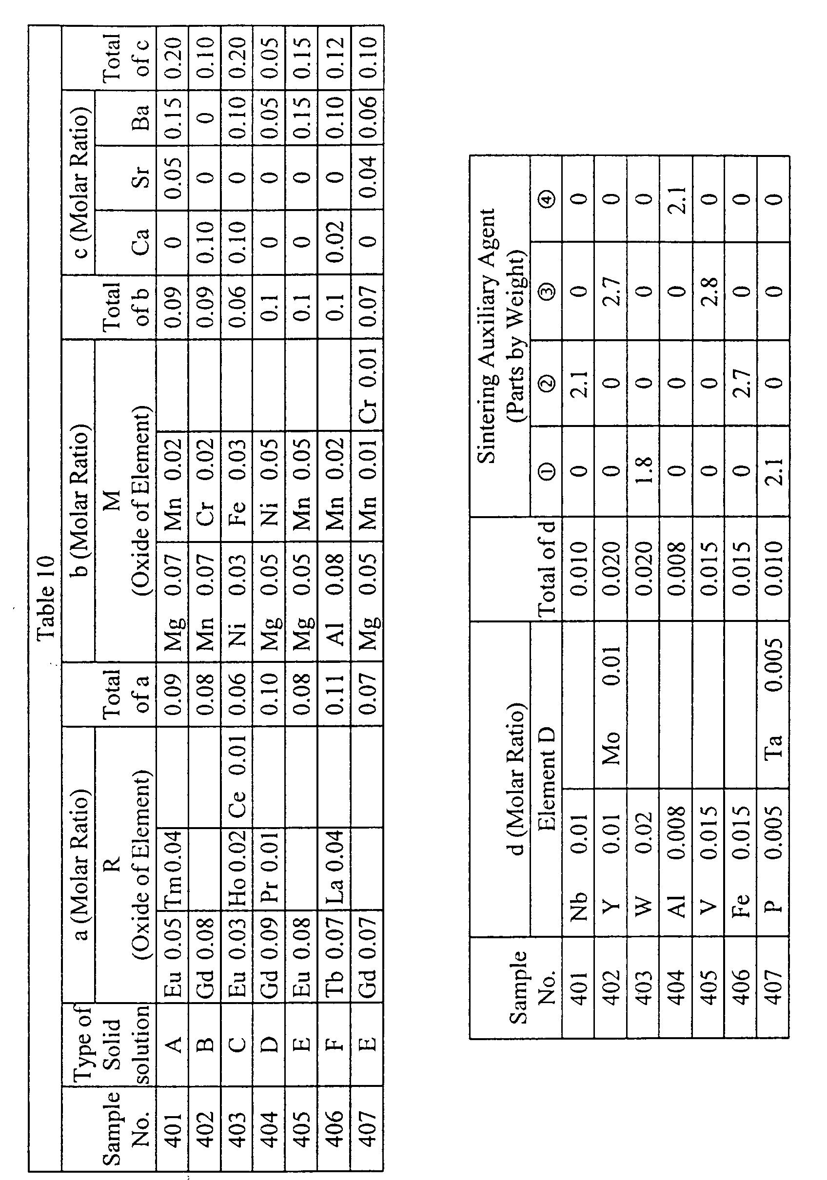
- Subsequently, in a manner equivalent to than in the first example, laminated ceramic capacitors to be used as samples were formed. In addition, in a manner equivalent to that in the first example, characteristics of the laminated ceramic capacitors and the dielectric ceramic compacts forming dielectric ceramic layers were measured. The results are shown in Table 11.

- In Tables 10 and 11, samples 401 and 402 were samples which were prepared by using barium titanates-based solid solution "A" and "B" shown in Table 9, respectively, in which at least one compound containing at least one element selected from the group consisting of S, Na and K in the form of SO3, Na2O, and K2O was contained at a content of more than about 0.5 part by weight with respect to 100 parts by weight of a barium titanate-based solid solution {(Ba1-x-ySrxCay)O}mTiO2, and sample 403 was prepared by using barium titanate-based solid solution "C" shown in Table 9 in which about 5 parts by weight or more of Cl was contained.
- According to samples 401 to 407, as shown in Tables 9 and 10, when the barium titanate-based solid solution was represented by the formula {(Ba1-x-ySrxCay)O}mTiO2 + aR + bM + cX(Zr,Hf)O3+ dD, x + y was in the range of from zero to about 0.20, a was in the range of from about 0.005 to 0.12, b was in the range of from about 0.005 to 0.12, c was about 0.20 or less, d was about 0.02 or less, m satisfied 1.000 < m ≤ 1.035, and in addition, the auxiliary sintering agent was contained in the range of from 0.2 to 4.0 parts by weight.
- According to samples 401 to 407, as shown in Table 11, sintering could be performed at 1,300°C or less, and hence, a base metal such as nickel could be used as the internal electrode material. In addition, the crystalline axis ratio c/a obtained by x-ray diffraction in a temperature range of -25°C or above satisfied 1.000 ≤ c/a ≤ 1.003.
- However, according to sample 401, since the content of S in the form of SO3 was more than about 0.5 part by weight, the continuity of the internal electrode was degraded, and hence, the evaluation could not be performed. As seen in the case of sample 402, when the contents of Na and K were more than 0.5 part by weight in the form of Na2O and K2O, respectively, the relative dielectric constant was decreased, and in addition, the average life time in the high temperature loading test was extremely decreased. In the case of sample 403, when the content of Cl was more than about 5 parts by weight, the relative dielectric constant was decreased, and the average life time in the high temperature loading test was extremely decreased.
- With samples 404 to 407, since the content of Na, S and K was less than about 0.5 part by weight in the form of Na2O, SO3 and K2O, respectively, and the content of Cl was less than about 5 parts by weight, the relative dielectric constant was more than 1,000, and the average life time in the high temperature loading test was more than 1,000 hours. In addition, the phase transition temperature was below -25°C; the CR product was high, such as more than 7,000 Ω·F; the heat generation (increase in temperature) was small, such as 14°C or less; the defect rate by the AC loading test could be suppressed to be 0%; and by the high temperature loading test, the average life time was increased to be more than 1,000 hours.
- In the first to the fifth examples described above, barium titanate-based powder prepared by a solid phase method was used; however, the present invention is not limited thereto, and for example, barium titanate-based material prepared by a wet method, such as an oxalic acid method, an alkoxide method or a hydrothermal synthetic method, may also be used. By using powder prepared by the latter method, characteristics improved than those obtained in the first to the fifth examples may be obtained in some cases.
- In addition, as starting materials for other than the barium titanate-based solid solution, various powdered oxides were used; however the present invention is not limited to those oxides, and instead of those described above, materials in the form of an alkoxide or an organic metal compound may also be used.
- Furthermore, in the examples described above, the phase transition temperature of a crystal forming a major portion of the dielectric ceramic compact was discussed, and even though the secondary phase is present, the practical characteristics will not be influenced.
- As has thus been described, according to the reduction-resistant dielectric ceramic compact of the present invention, since firing at 1,300°C or less in a non-oxidizing atmosphere can be performed, a base metal such as nickel, a nickel alloy, copper, or a copper alloy can be used as the internal electrode material in the laminated ceramic capacitor formed of this dielectric ceramic compact.
- According to the reduction-resistant dielectric ceramic compact of the present invention, in addition to a sufficient relative dielectric constant of 700 or more, the loss and the heat generation are low under high frequency conditions of high voltage or large current, and superior resistant characteristics under AC or DC high temperature loading conditions, that is, a stable insulating resistance, can be obtained. Consequently, when a laminated ceramic capacitor is formed of this dielectric ceramic compact, the reliability of the laminated ceramic capacitor can be improved.
Claims (21)
- A reduction-resistant dielectric ceramic compact comprising:a solid solution comprising barium titanate as a primary component and an auxiliary sintering agent which has an x-ray diffraction crystalline axis ratio c/a in a temperature range of -25°C or above of 1.000 ≤ c/a ≤ 1.003 and a maximum peak for temperature dependence of a dielectric constant measured at an electric strength of 2 Vrms/mm or less and at an AC frequency of 1 kHz at a temperature of below -25°C,wherein the primary component is represented by the formulaABO3 is a barium titanate-based perovskite compound having A-site and B-site elements such that 1.000 < A/B ≤ 1.035,R is a compound containing at least one element selected from the group consisting of La, Ce, Pr, Nd, Sm, Eu, Gd, Tb, Dy, Ho, Er, Tm, Yb and Lu,M is a compound containing at least one element selected from the group consisting of Mn, Ni, Mg, Fe, Al, Cr and Zn,and a and b are in moles such that 0.005 ≤ a ≤ 0.12, and 0.005 ≤ b ≤ 0.12.
- A reduction-resistant dielectric ceramic compact according to Claim 1, wherein the auxiliary sintering agent is about 0.2 to 4 parts by weight with respect to 100 parts by weight of the primary component.
- A reduction-resistant dielectric ceramic compact according to Claim 1, wherein the primary component comprises X(Zr,Hf)O3 in which X is at least one element selected from the group consisting of Ba, Sr and Ca.
- A reduction-resistant dielectric ceramic compact according to Claim 3, wherein the amount of X(Zr,Hf)O3 is greater than zero up to about 0.20 mole with respect to 1 mole of the ABO3 in the primary component.
- A reduction-resistant dielectric ceramic compact according to Claim 1, wherein the primary component further comprises a compound D containing at least one element selected from the group consisting of V, Nb, Ta, Mo, W, Y, Sc, P, Al and Fe.
- A reduction-resistant dielectric ceramic compact according to Claim 5, wherein the amount of D is more than zero up to about 0.02 mole with respect to 1 mole of the ABO3 in the primary component.
- A reduction-resistant dielectric ceramic compact according to Claim 5, wherein the primary component comprises X(Zr,Hf)O3 in which X is at least one element selected from the group consisting of Ba, Sr and Ca.
- A reduction-resistant dielectric ceramic compact according to Claim 3, wherein the amount of X(Zr,Hf)O3 and the amount of D are each greater than zero up to about 0.20 mole with respect to 1 mole of the ABO3 in the primary component.
- A reduction-resistant dielectric ceramic compact according to Claim 8, whereinABO3 is a barium titanate-based perovskite compound represented by the formula {(Ba1-x-ySrxCay)O}mTiO2 in which 0 ≤ x + y ≤ 0.20 and 1.000 < m ≤ 1.035, and the auxiliary sintering agent is selected from the group consisting of a compound containing boron, a compound containing silicon and a compound containing boron and silicon, andwhich further comprises, with respect to 100 parts by weight of the barium titanate-based perovskite compound, a positive amount up to about 0.5 part of a compound containing at least one element selected from the group consisting of S, Na and K, and a positive amount up to about 5 parts of a compound containing Cl.
- A reduction-resistant dielectric ceramic compact according to Claim 1, whereinABO3 is a barium titanate-based perovskite compound represented by the formula {(Ba1-x-ySrxCay)O}mTiO2 in which 0 ≤ x + y ≤ 0.20 and 1.000 < m ≤ 1.035, andfurther comprises, with respect to 100 parts by weight of the barium titanate-based perovskite compound, a positive amount up to about 0.5 part of a compound containing at least one element selected from the group consisting of S, Na and K, and a positive amount up to about 5 parts of a compound containing Cl.
- A reduction-resistant dielectric ceramic compact according to Claim 1, wherein the auxiliary sintering agent is selected from the group consisting of a compound containing boron, a compound containing silicon and a compound containing boron and silicon.
- A reduction-resistant dielectric ceramic compact according to Claim 11, wherein the compound containing silicon is silicon oxide.
- A laminated ceramic capacitor comprising:wherein the dielectric ceramic layers comprise a reduction-resistant dielectric ceramic compact according to Claim 9.a plurality of dielectric ceramic layers;a plurality of internal electrodes each of which sandwiches at least a part of a dielectric ceramic layer; anda pair of external electrodes electrically connected to the internal electrodes,
- A laminated ceramic capacitor according to Claim 13, wherein the internal electrodes comprise nickel, a nickel alloy, copper or a copper alloy.
- A laminated ceramic capacitor according to Claim 14, wherein each external electrodes comprises a first sintered layer comprising a powdered conductive metal and optionally glass frit, crystallized glass or ceramic; and a second layer disposed on the first layer and which is a plating layer.
- A laminated ceramic capacitor comprising:wherein the dielectric ceramic layers comprise a reduction-resistant dielectric ceramic compact according to Claim 7.a plurality of dielectric ceramic layers;a plurality of internal electrodes each of which sandwiches at least a part of a dielectric ceramic layer; anda pair of external electrodes electrically connected to the internal electrodes,
- A laminated ceramic capacitor according to Claim 16, wherein the internal electrodes comprise nickel, a nickel alloy, copper or a copper alloy.
- A laminated ceramic capacitor according to Claim 17, wherein each external electrodes comprises a first sintered layer comprising a powdered conductive metal and optionally glass frit, crystallized glass or ceramic; and a second layer disposed on the first layer and which is a plating layer.
- A laminated ceramic capacitor comprising:wherein the dielectric ceramic layers comprise a reduction-resistant dielectric ceramic compact according to Claim 1.a plurality of dielectric ceramic layers;a plurality of internal electrodes each of which sandwiches at least a part of a dielectric ceramic layer; anda pair of external electrodes electrically connected to the internal electrodes,
- A laminated ceramic capacitor according to Claim 19, wherein the internal electrodes comprise nickel, a nickel alloy, copper or a copper alloy.
- A laminated ceramic capacitor according to Claim 21, wherein each external electrodes comprises a first sintered layer comprising a powdered conductive metal and optionally glass frit, crystallized glass or ceramic; and a second layer disposed on the first layer and which is a plating layer.
Applications Claiming Priority (2)
| Application Number | Priority Date | Filing Date | Title |
|---|---|---|---|
| JP2000231084 | 2000-07-31 | ||
| JP2000231084A JP2002050536A (en) | 2000-07-31 | 2000-07-31 | Reduction-resistant dielectric ceramic and laminated ceramic capacitor |
Publications (2)
| Publication Number | Publication Date |
|---|---|
| EP1178024A2 true EP1178024A2 (en) | 2002-02-06 |
| EP1178024A3 EP1178024A3 (en) | 2004-03-03 |
Family
ID=18723958
Family Applications (1)
| Application Number | Title | Priority Date | Filing Date |
|---|---|---|---|
| EP01116386A Withdrawn EP1178024A3 (en) | 2000-07-31 | 2001-07-06 | Reduction-resistant dielectric ceramic compact and laminated ceramic capacitor |
Country Status (5)
| Country | Link |
|---|---|
| US (1) | US6522521B2 (en) |
| EP (1) | EP1178024A3 (en) |
| JP (1) | JP2002050536A (en) |
| KR (1) | KR100438517B1 (en) |
| TW (1) | TW493188B (en) |
Cited By (3)
| Publication number | Priority date | Publication date | Assignee | Title |
|---|---|---|---|---|
| US8179660B2 (en) | 2005-03-06 | 2012-05-15 | Murata Manufacturing Co., Ltd. | Electronic device and method for manufacturing the same |
| CN103113100A (en) * | 2013-03-01 | 2013-05-22 | 江苏大学 | High-temperature stabilization ceramic capacitor dielectric |
| CN103354672A (en) * | 2013-07-02 | 2013-10-16 | 中国核动力研究设计院 | Heating device simulating multiple kinds of heat flux density distribution patterns |
Families Citing this family (65)
| Publication number | Priority date | Publication date | Assignee | Title |
|---|---|---|---|---|
| JP4311124B2 (en) * | 2002-09-10 | 2009-08-12 | 株式会社村田製作所 | Chip-type electronic components |
| JP4003735B2 (en) * | 2002-11-22 | 2007-11-07 | 株式会社村田製作所 | Calculation method of active power related to capacitor, measurement method of active power consumed by capacitor, capacitor selection method, calculation device of active power related to capacitor, and recording medium recording the calculation program |
| JP4110978B2 (en) * | 2003-01-24 | 2008-07-02 | 株式会社村田製作所 | Dielectric ceramic, manufacturing method thereof, and multilayer ceramic capacitor |
| TWI240288B (en) * | 2003-01-31 | 2005-09-21 | Murata Manufacturing Co | Dielectric ceramic and the manufacturing method thereof, and the laminated ceramic condenser |
| JP4513278B2 (en) * | 2003-05-26 | 2010-07-28 | 株式会社村田製作所 | Non-reducing dielectric ceramic manufacturing method, non-reducing dielectric ceramic and multilayer ceramic capacitor |
| CN1922118B (en) | 2004-02-27 | 2011-08-17 | 株式会社村田制作所 | Dielectric ceramic composition and laminated ceramic capacitor |
| JP4506233B2 (en) * | 2004-03-30 | 2010-07-21 | 株式会社村田製作所 | Dielectric ceramic and multilayer ceramic capacitors |
| WO2005104148A1 (en) * | 2004-04-23 | 2005-11-03 | Murata Manufacturing Co., Ltd. | Electronic component and manufacturing method thereof |
| JP4095586B2 (en) * | 2004-06-29 | 2008-06-04 | Tdk株式会社 | Multilayer ceramic capacitor and manufacturing method thereof |
| WO2006006333A1 (en) | 2004-07-08 | 2006-01-19 | Murata Manufacturing Co., Ltd. | Dielectric ceramic composition and laminated ceramic capacitor |
| JP2006041393A (en) * | 2004-07-29 | 2006-02-09 | Tdk Corp | Multilayer ceramic capacitor |
| JP4370217B2 (en) * | 2004-07-29 | 2009-11-25 | Tdk株式会社 | Multilayer ceramic capacitor |
| US7365958B2 (en) * | 2004-10-27 | 2008-04-29 | Kyocera Corporation | Dielectric ceramics, multilayer ceramic capacitor and method for manufacturing the same |
| JP4548423B2 (en) * | 2004-12-24 | 2010-09-22 | 株式会社村田製作所 | Dielectric ceramic and multilayer ceramic capacitors |
| JP4622537B2 (en) * | 2005-01-20 | 2011-02-02 | Tdk株式会社 | Dielectric porcelain composition and electronic component |
| CN100391896C (en) * | 2005-05-13 | 2008-06-04 | 中国科学院上海硅酸盐研究所 | Hafnium oxide-gadolinium oxide solid solution transparent ceramic glaring material and its preparation method and uses |
| JP4752327B2 (en) * | 2005-05-17 | 2011-08-17 | 株式会社村田製作所 | Dielectric ceramic composition and multilayer ceramic capacitor |
| JP3901196B2 (en) * | 2005-05-26 | 2007-04-04 | 株式会社村田製作所 | Multilayer ceramic electronic components |
| KR100691437B1 (en) * | 2005-11-02 | 2007-03-09 | 삼성전기주식회사 | Polymer-ceramic composition for dielectrics, embedded capacitor and printed circuit board using the same |
| JP4782552B2 (en) * | 2005-11-28 | 2011-09-28 | 京セラ株式会社 | Dielectric porcelain |
| JP2007234828A (en) * | 2006-02-28 | 2007-09-13 | Tdk Corp | Electronic component and manufacturing method thereof |
| JP2007297258A (en) * | 2006-04-28 | 2007-11-15 | Taiyo Yuden Co Ltd | Dielectric ceramic and laminated ceramic capacitor |
| JP4936825B2 (en) * | 2006-08-02 | 2012-05-23 | 太陽誘電株式会社 | Multilayer ceramic capacitor |
| WO2008035727A1 (en) * | 2006-09-22 | 2008-03-27 | Murata Manufacturing Co., Ltd. | Laminated ceramic capacitor |
| JP4863005B2 (en) * | 2006-12-27 | 2012-01-25 | Tdk株式会社 | Dielectric porcelain composition and electronic component |
| JP4863007B2 (en) * | 2007-01-23 | 2012-01-25 | Tdk株式会社 | Dielectric porcelain composition and electronic component |
| WO2008123139A1 (en) * | 2007-03-26 | 2008-10-16 | Murata Manufacturing Co., Ltd. | Resistance memory element |
| JP5034839B2 (en) * | 2007-04-12 | 2012-09-26 | Tdk株式会社 | Dielectric porcelain composition and electronic component |
| TW201245098A (en) * | 2007-09-28 | 2012-11-16 | Tdk Corp | Dielectric ceramic composition and electronic device |
| JP4967963B2 (en) * | 2007-09-28 | 2012-07-04 | Tdk株式会社 | Dielectric porcelain composition and electronic component |
| JP4710908B2 (en) * | 2008-01-10 | 2011-06-29 | Tdk株式会社 | Dielectric porcelain composition and electronic component |
| JP5061961B2 (en) * | 2008-03-04 | 2012-10-31 | Tdk株式会社 | Dielectric porcelain composition |
| JP4959634B2 (en) * | 2008-03-26 | 2012-06-27 | 京セラ株式会社 | Dielectric porcelain and capacitor |
| JP5217609B2 (en) * | 2008-05-12 | 2013-06-19 | 株式会社村田製作所 | Multilayer ceramic electronic component and manufacturing method thereof |
| JP5115349B2 (en) * | 2008-06-13 | 2013-01-09 | 株式会社村田製作所 | Multilayer ceramic electronic component and manufacturing method thereof |
| EP2326239B1 (en) | 2008-07-03 | 2017-06-21 | Masimo Laboratories, Inc. | Protrusion for improving spectroscopic measurement of blood constituents |
| US8630691B2 (en) | 2008-08-04 | 2014-01-14 | Cercacor Laboratories, Inc. | Multi-stream sensor front ends for noninvasive measurement of blood constituents |
| JP2010040798A (en) * | 2008-08-06 | 2010-02-18 | Murata Mfg Co Ltd | Stacked ceramic capacitor |
| WO2010047181A1 (en) | 2008-10-21 | 2010-04-29 | 株式会社村田製作所 | Dielectric ceramic and laminated ceramic capacitor |
| JP5067401B2 (en) * | 2009-06-30 | 2012-11-07 | 株式会社村田製作所 | Dielectric ceramic, manufacturing method thereof, and multilayer ceramic capacitor |
| JP5330126B2 (en) * | 2009-07-06 | 2013-10-30 | 株式会社デンソー | Ceramic materials and capacitors |
| JP5293506B2 (en) * | 2009-08-31 | 2013-09-18 | Tdk株式会社 | Ceramic electronic component and method for manufacturing ceramic electronic component |
| US8688183B2 (en) | 2009-09-03 | 2014-04-01 | Ceracor Laboratories, Inc. | Emitter driver for noninvasive patient monitor |
| JP4894908B2 (en) * | 2009-11-17 | 2012-03-14 | Tdk株式会社 | Dielectric porcelain composition |
| KR101070068B1 (en) * | 2009-12-24 | 2011-10-04 | 삼성전기주식회사 | multilayer ceramic capacitor |
| JP5224147B2 (en) * | 2010-09-28 | 2013-07-03 | 株式会社村田製作所 | Dielectric ceramic and multilayer ceramic capacitor |
| JP2013048231A (en) * | 2011-08-29 | 2013-03-07 | Samsung Electro-Mechanics Co Ltd | Laminated ceramic electronic component and manufacturing method therefor |
| JP5910317B2 (en) * | 2012-05-28 | 2016-04-27 | Tdk株式会社 | Dielectric porcelain composition and electronic component |
| KR20150032840A (en) * | 2012-06-21 | 2015-03-30 | 트로피 | Method for production of a pellet for a direct-conversion detector of x-rays, direct-conversion detector of x-rays and dental radiology apparatus using such a detector |
| JP5994853B2 (en) * | 2012-07-10 | 2016-09-21 | 株式会社村田製作所 | Multilayer ceramic capacitor and manufacturing method thereof |
| KR20140083509A (en) * | 2012-12-26 | 2014-07-04 | 삼성전기주식회사 | Dielectric composition, and multilayer ceramic capacitor comprising dielectric layer the same |
| KR20140125111A (en) * | 2013-04-18 | 2014-10-28 | 삼성전기주식회사 | Multi-layered ceramic electronic part, manufacturing method thereof and board for mounting the same |
| KR101589687B1 (en) * | 2013-10-31 | 2016-01-29 | 알에프엠엔씨 주식회사 | Dielectric Ceramic Compositions for High Frequency and the Manufacturing Method of the Same |
| KR101983154B1 (en) * | 2013-11-05 | 2019-05-28 | 삼성전기주식회사 | Multi-Layered Ceramic Capacitor |
| US10569330B2 (en) * | 2014-04-01 | 2020-02-25 | Forge Nano, Inc. | Energy storage devices having coated passive components |
| US10918827B2 (en) | 2015-07-20 | 2021-02-16 | Strataca Systems Limited | Catheter device and method for inducing negative pressure in a patient's bladder |
| JP6696267B2 (en) * | 2016-03-30 | 2020-05-20 | Tdk株式会社 | Dielectric ceramic composition and multilayer ceramic capacitor |
| KR102653205B1 (en) | 2016-11-23 | 2024-04-01 | 삼성전기주식회사 | Multi-layered capacitor and board having the same mounted thereon |
| US10593475B2 (en) * | 2017-09-22 | 2020-03-17 | Taiyo Yuden Co., Ltd. | Multi-layer ceramic capacitor |
| JP2019134098A (en) * | 2018-01-31 | 2019-08-08 | Tdk株式会社 | Multilayer ceramic capacitor |
| JP7145652B2 (en) * | 2018-06-01 | 2022-10-03 | 太陽誘電株式会社 | Multilayer ceramic capacitor and manufacturing method thereof |
| JP7446705B2 (en) | 2018-06-12 | 2024-03-11 | 太陽誘電株式会社 | Multilayer ceramic capacitor and its manufacturing method |
| KR102292797B1 (en) * | 2019-02-13 | 2021-08-24 | 삼성전기주식회사 | Dielectric ceramic composition and multilayer ceramic capacitor comprising the same |
| CN111170735B (en) * | 2020-01-14 | 2022-03-18 | 西安工业大学 | Ceramic material with high electric energy storage efficiency and preparation method thereof |
| JP2022156320A (en) * | 2021-03-31 | 2022-10-14 | Tdk株式会社 | Multilayer electronic component |
Citations (4)
| Publication number | Priority date | Publication date | Assignee | Title |
|---|---|---|---|---|
| DE19902153A1 (en) * | 1998-01-20 | 1999-07-22 | Murata Manufacturing Co | Dielectric ceramic for a laminated ceramic electronic element e.g. a miniature capacitor |
| EP0977217A1 (en) * | 1998-05-12 | 2000-02-02 | Murata Manufacturing Co., Ltd. | Dielectric ceramic composition and laminated ceramic capacitor |
| EP0992469A2 (en) * | 1998-09-28 | 2000-04-12 | Murata Manufacturing Co., Ltd. | Dielectric ceramic composition and monolithic ceramic capacitor |
| EP1056102A2 (en) * | 1999-05-24 | 2000-11-29 | Murata Manufacturing Co., Ltd. | Nonreducing dielectric ceramic and monolithic ceramic capacitor |
Family Cites Families (18)
| Publication number | Priority date | Publication date | Assignee | Title |
|---|---|---|---|---|
| US4283753A (en) * | 1979-09-28 | 1981-08-11 | Sprague Electric Company | Low firing monolithic ceramic capacitor with high dielectric constant |
| JPS59184511A (en) * | 1983-04-04 | 1984-10-19 | 株式会社村田製作所 | Ceramic laminated condenser |
| JPS6114611A (en) | 1984-06-29 | 1986-01-22 | Fujitsu Ltd | Reinforcing method of connecting part of optical fiber |
| JP2848712B2 (en) | 1991-02-20 | 1999-01-20 | 太陽誘電株式会社 | Dielectric porcelain composition |
| JPH07118431B2 (en) | 1991-03-16 | 1995-12-18 | 太陽誘電株式会社 | Porcelain capacitor and method of manufacturing the same |
| JPH05109319A (en) | 1991-10-17 | 1993-04-30 | Tdk Corp | High dielectric constant dielectric porcilain composition |
| JP3269903B2 (en) | 1993-12-29 | 2002-04-02 | 太陽誘電株式会社 | Porcelain capacitor and method of manufacturing the same |
| JP3250923B2 (en) | 1994-11-28 | 2002-01-28 | 京セラ株式会社 | Dielectric porcelain composition |
| JP3269908B2 (en) | 1994-03-30 | 2002-04-02 | 太陽誘電株式会社 | Porcelain capacitor and method of manufacturing the same |
| JP3326513B2 (en) | 1994-10-19 | 2002-09-24 | ティーディーケイ株式会社 | Multilayer ceramic chip capacitors |
| JP3024536B2 (en) * | 1995-12-20 | 2000-03-21 | 株式会社村田製作所 | Multilayer ceramic capacitors |
| JP3039397B2 (en) * | 1996-01-18 | 2000-05-08 | 株式会社村田製作所 | Dielectric ceramic composition and multilayer ceramic capacitor using the same |
| JP2998639B2 (en) * | 1996-06-20 | 2000-01-11 | 株式会社村田製作所 | Multilayer ceramic capacitors |
| DE19737324A1 (en) * | 1997-08-28 | 1999-03-04 | Philips Patentverwaltung | Multi-layer capacitor with silver and rare earth doped barium titanate |
| JP3391269B2 (en) * | 1998-01-20 | 2003-03-31 | 株式会社村田製作所 | Dielectric ceramic and its manufacturing method, and multilayer ceramic electronic component and its manufacturing method |
| JP3344314B2 (en) * | 1998-04-08 | 2002-11-11 | 株式会社村田製作所 | Pulse generation capacitor |
| JP3019854B1 (en) * | 1998-09-28 | 2000-03-13 | 松下電器産業株式会社 | Dielectric ceramic composition, multilayer ceramic capacitor using the same, and method of manufacturing the same |
| JP2001126946A (en) * | 1999-10-28 | 2001-05-11 | Murata Mfg Co Ltd | Laminated ceramic electronic component and method for manufacturing the same |
-
2000
- 2000-07-31 JP JP2000231084A patent/JP2002050536A/en active Pending
-
2001
- 2001-06-27 TW TW090115599A patent/TW493188B/en not_active IP Right Cessation
- 2001-07-06 EP EP01116386A patent/EP1178024A3/en not_active Withdrawn
- 2001-07-31 KR KR10-2001-0046268A patent/KR100438517B1/en active IP Right Grant
- 2001-07-31 US US09/919,409 patent/US6522521B2/en not_active Expired - Lifetime
Patent Citations (4)
| Publication number | Priority date | Publication date | Assignee | Title |
|---|---|---|---|---|
| DE19902153A1 (en) * | 1998-01-20 | 1999-07-22 | Murata Manufacturing Co | Dielectric ceramic for a laminated ceramic electronic element e.g. a miniature capacitor |
| EP0977217A1 (en) * | 1998-05-12 | 2000-02-02 | Murata Manufacturing Co., Ltd. | Dielectric ceramic composition and laminated ceramic capacitor |
| EP0992469A2 (en) * | 1998-09-28 | 2000-04-12 | Murata Manufacturing Co., Ltd. | Dielectric ceramic composition and monolithic ceramic capacitor |
| EP1056102A2 (en) * | 1999-05-24 | 2000-11-29 | Murata Manufacturing Co., Ltd. | Nonreducing dielectric ceramic and monolithic ceramic capacitor |
Cited By (7)
| Publication number | Priority date | Publication date | Assignee | Title |
|---|---|---|---|---|
| US8179660B2 (en) | 2005-03-06 | 2012-05-15 | Murata Manufacturing Co., Ltd. | Electronic device and method for manufacturing the same |
| CN101189693B (en) * | 2005-06-03 | 2012-11-07 | 株式会社村田制作所 | Electronic device and method for manufacturing the same |
| US8894836B2 (en) | 2005-06-03 | 2014-11-25 | Murata Manufacturing Co., Ltd. | Electronic device and method for manufacturing the same |
| CN103113100A (en) * | 2013-03-01 | 2013-05-22 | 江苏大学 | High-temperature stabilization ceramic capacitor dielectric |
| CN103113100B (en) * | 2013-03-01 | 2014-10-29 | 江苏大学 | High-temperature stabilization ceramic capacitor dielectric |
| CN103354672A (en) * | 2013-07-02 | 2013-10-16 | 中国核动力研究设计院 | Heating device simulating multiple kinds of heat flux density distribution patterns |
| CN103354672B (en) * | 2013-07-02 | 2016-03-23 | 中国核动力研究设计院 | A kind of electro-heat equipment of simulating multiple heat flux distribution |
Also Published As
| Publication number | Publication date |
|---|---|
| KR20020011120A (en) | 2002-02-07 |
| TW493188B (en) | 2002-07-01 |
| US6522521B2 (en) | 2003-02-18 |
| KR100438517B1 (en) | 2004-07-03 |
| EP1178024A3 (en) | 2004-03-03 |
| US20020039272A1 (en) | 2002-04-04 |
| JP2002050536A (en) | 2002-02-15 |
Similar Documents
| Publication | Publication Date | Title |
|---|---|---|
| US6522521B2 (en) | Reduction-resistant dielectric ceramic compact and laminated ceramic capacitor | |
| KR100326951B1 (en) | Dielectric ceramic composition and monolithic ceramic capacitor | |
| KR100313234B1 (en) | Dielectric Ceramic Composition and Laminated Ceramic Capacitor | |
| EP0851444B1 (en) | Ceramic composition and multilayer ceramic capacitor made therefrom | |
| KR100259321B1 (en) | Dielectric ceramic composition and monolitic ceramic capacitor using the same | |
| EP0858086B1 (en) | Monolithic ceramic capacitor | |
| US6900977B2 (en) | Dielectric ceramic, manufacturing method thereof, and multilayer ceramic capacitor | |
| KR100256199B1 (en) | Monolithic ceramic capacitor | |
| KR100326950B1 (en) | Dielectric ceramic composition and laminated ceramic parts | |
| JP2001143955A (en) | Dielectric ceramic composition and laminated ceramic capacitor | |
| US6385035B1 (en) | Dielectric ceramic composition and monolithic ceramic component | |
| JPH1012479A (en) | Laminated ceramics capacitor | |
| JPH09171938A (en) | Multilayered ceramic capacitor | |
| JPH09232180A (en) | Laminated ceramic capacitor | |
| KR980009197A (en) | Multilayer Ceramic Capacitors | |
| JP3039409B2 (en) | Multilayer ceramic capacitors | |
| JP3039426B2 (en) | Multilayer ceramic capacitors | |
| US6259594B1 (en) | Nonreducing dielectric ceramic and monolithic ceramic capacitor | |
| JP3678072B2 (en) | Dielectric ceramic composition and multilayer ceramic component | |
| JP3678073B2 (en) | Dielectric ceramic composition and multilayer ceramic component | |
| JP4258172B2 (en) | Multilayer ceramic capacitor | |
| JPH10172857A (en) | Laminated layer ceramics capacitor | |
| JPH10172858A (en) | Laminated layer ceramics capacitor |
Legal Events
| Date | Code | Title | Description |
|---|---|---|---|
| PUAI | Public reference made under article 153(3) epc to a published international application that has entered the european phase |
Free format text: ORIGINAL CODE: 0009012 |
|
| 17P | Request for examination filed |
Effective date: 20010706 |
|
| AK | Designated contracting states |
Kind code of ref document: A2 Designated state(s): AT BE CH CY DE DK ES FI FR GB GR IE IT LI LU MC NL PT SE TR |
|
| AX | Request for extension of the european patent |
Free format text: AL;LT;LV;MK;RO;SI |
|
| PUAL | Search report despatched |
Free format text: ORIGINAL CODE: 0009013 |
|
| AK | Designated contracting states |
Kind code of ref document: A3 Designated state(s): AT BE CH CY DE DK ES FI FR GB GR IE IT LI LU MC NL PT SE TR |
|
| AX | Request for extension of the european patent |
Extension state: AL LT LV MK RO SI |
|
| 17Q | First examination report despatched |
Effective date: 20040416 |
|
| AKX | Designation fees paid |
Designated state(s): DE FR GB |
|
| STAA | Information on the status of an ep patent application or granted ep patent |
Free format text: STATUS: THE APPLICATION IS DEEMED TO BE WITHDRAWN |
|
| 18D | Application deemed to be withdrawn |
Effective date: 20041027 |