EP1176634A2 - Verfahren zum anisotropen Trockenätzen von organischer Antireflexionsschichten - Google Patents
Verfahren zum anisotropen Trockenätzen von organischer Antireflexionsschichten Download PDFInfo
- Publication number
- EP1176634A2 EP1176634A2 EP01115152A EP01115152A EP1176634A2 EP 1176634 A2 EP1176634 A2 EP 1176634A2 EP 01115152 A EP01115152 A EP 01115152A EP 01115152 A EP01115152 A EP 01115152A EP 1176634 A2 EP1176634 A2 EP 1176634A2
- Authority
- EP
- European Patent Office
- Prior art keywords
- etching
- layer
- nitrogen
- hydrogen
- organic anti
- Prior art date
- Legal status (The legal status is an assumption and is not a legal conclusion. Google has not performed a legal analysis and makes no representation as to the accuracy of the status listed.)
- Withdrawn
Links
Images



Classifications
-
- H—ELECTRICITY
- H10—SEMICONDUCTOR DEVICES; ELECTRIC SOLID-STATE DEVICES NOT OTHERWISE PROVIDED FOR
- H10P—GENERIC PROCESSES OR APPARATUS FOR THE MANUFACTURE OR TREATMENT OF DEVICES COVERED BY CLASS H10
- H10P76/00—Manufacture or treatment of masks on semiconductor bodies, e.g. by lithography or photolithography
- H10P76/20—Manufacture or treatment of masks on semiconductor bodies, e.g. by lithography or photolithography of masks comprising organic materials
- H10P76/204—Manufacture or treatment of masks on semiconductor bodies, e.g. by lithography or photolithography of masks comprising organic materials of organic photoresist masks
- H10P76/2041—Photolithographic processes
- H10P76/2043—Photolithographic processes using an anti-reflective coating
-
- H—ELECTRICITY
- H10—SEMICONDUCTOR DEVICES; ELECTRIC SOLID-STATE DEVICES NOT OTHERWISE PROVIDED FOR
- H10P—GENERIC PROCESSES OR APPARATUS FOR THE MANUFACTURE OR TREATMENT OF DEVICES COVERED BY CLASS H10
- H10P50/00—Etching of wafers, substrates or parts of devices
- H10P50/20—Dry etching; Plasma etching; Reactive-ion etching
- H10P50/28—Dry etching; Plasma etching; Reactive-ion etching of insulating materials
- H10P50/286—Dry etching; Plasma etching; Reactive-ion etching of insulating materials of organic materials
- H10P50/287—Dry etching; Plasma etching; Reactive-ion etching of insulating materials of organic materials by chemical means
-
- G—PHYSICS
- G03—PHOTOGRAPHY; CINEMATOGRAPHY; ANALOGOUS TECHNIQUES USING WAVES OTHER THAN OPTICAL WAVES; ELECTROGRAPHY; HOLOGRAPHY
- G03F—PHOTOMECHANICAL PRODUCTION OF TEXTURED OR PATTERNED SURFACES, e.g. FOR PRINTING, FOR PROCESSING OF SEMICONDUCTOR DEVICES; MATERIALS THEREFOR; ORIGINALS THEREFOR; APPARATUS SPECIALLY ADAPTED THEREFOR
- G03F7/00—Photomechanical, e.g. photolithographic, production of textured or patterned surfaces, e.g. printing surfaces; Materials therefor, e.g. comprising photoresists; Apparatus specially adapted therefor
- G03F7/004—Photosensitive materials
- G03F7/09—Photosensitive materials characterised by structural details, e.g. supports, auxiliary layers
- G03F7/091—Photosensitive materials characterised by structural details, e.g. supports, auxiliary layers characterised by antireflection means or light filtering or absorbing means, e.g. anti-halation, contrast enhancement
Definitions
- the invention relates to a method for anisotropic dry etching an organic anti-reflection layer.
- Integrated circuits on semiconductor wafers are manufactured using planar technology.
- the structuring of the semiconductor layers for training the individual components are carried out almost consistently with the help of lithographic technology.
- the desired component structures are first in a photo mask in a thin, radiation-sensitive film, usually an organic one Photoresist layer on the oxidized semiconductor wafer generated and with the help of special etching processes in the underlying layers transferred. Irradiation of the Photoresist layer takes place with narrow-band light, whereby before all high-pressure mercury lamps or lasers are used. However, the exposure is often pronounced Interference effects between the incident and the Semiconductor wafers reflected light waves that lead to line width fluctuations of light on the photoresist layer. Reduce this line width fluctuation or enlarge the one transferred to the photoresist with the mask Structure in an undesirable way.
- Anti-reflection layers are used to reduce the interference effects between the semiconductor substrate and the photoresist layer applied, which from the semiconductor substrate in the Absorb photoresist layer back-reflected light waves or wipe out by destructive interference.
- antireflection layers consisting of organic polymers used, which is characterized by high light absorption distinguished.
- Organic anti-reflective layers are suitable also to planarize edges and Steps in the semiconductor layers. Such a leveling is often especially before the application of a metal level in which Conductor tracks for wiring the components of the semiconductor chip trained, required. Because of the limited Conformity of the commonly used metal sputter coating can namely the thickness of the metallization steep edges on the semiconductor surface be so low that the conductor cross-sections are significantly smaller than on planar surfaces fail.
- a variant of the photoresist technology with an anti-reflection layer is the so-called trilevel resist technique.
- bottom resist layer on the semiconductor substrate spun on, which is a positive resist or its resin, that by an absorber additive or by high heating can be made highly light absorbing.
- Bottom resist layer becomes a spin-on-glass intermediate layer and then a so-called top resist layer applied.
- This top-most resist layer is actually that photochemically active layer.
- the bottom resist layer on the other hand ensures that practically no light from the semiconductor substrate reflected back into this top resist layer becomes.
- the bottom resist layer also becomes sufficient made thick to exist on the semiconductor substrate level steep steps so that the top resist layer with one that is unaffected by these surface levels Thickness can be thrown out.
- the top resist layer is then over a mask that the desired Semiconductor device structure contains, exposed and developed.
- the top resist layer is loosened by the development exposed areas, but the non-irradiated areas stay masked.
- the spin-on-glass intermediate layer etched at the exposed areas. Latter then serves as an etching mask during anisotropic etching of the bottom resist layer, which in turn is a masking layer for etching the underlying structure Semiconductor layer, e.g. Silicon dioxide is used.
- a Bilevel resist technology are used, in which on the Spin-on glass intermediate layer is dispensed with. Then this is possible if the top resist structure is resistant to etching the bottom resist etch is.
- the organic anti-reflection layer is opened conventionally using dry etching techniques, whereby the following requirements are placed on the etching process:
- the anisotropy factor of the etching should be as close as possible to 1 to ensure high profile accuracy, i.e. steep paint flanks achieve.
- the mask structure should be as precise as possible on the one under the organic anti-reflection layer Semiconductor layer are transferred, i.e. the etching is said to be CD (Critical Dimension) be loyal.
- CD Cosmetic Dimension
- the dry etching process usually uses gaseous media, through a gas discharge in a high-frequency alternating field be stimulated.
- the discharge process takes place in the vacuum area instead, so that a large free path length of the ions between two bumps.
- chemical-physical Dry etching process used, in which in addition to a purely physical Material removal by knocking out atoms or Molecules from the layer to be etched a chemical material removal done by a reactive gas.
- the most important Etching process in chemical-physical dry etching is the reactive ion etching, with anisotropic etching of organic anti-reflection layer as the reaction gas all oxygen is used because oxygen with the polymer components forms volatile reaction products.
- a physical-chemical dry etching with an oxygen-chlorine chemistry is characterized by a structurally accurate Transfer of the mask structure in the etching process to the below the organic anti-reflection layer semiconductor structure out.
- the profile accuracy is low and in addition, an undesirable co-etching of the semiconductor layer occurs on.
- an oxygen-nitrogen chemistry for chemical-physical dry etching of an organic Antireflection coating can improve selectivity to the semiconductor substrate under the anti-reflection layer achieved, but CD loyalty is low.
- Etching the organic anti-reflection layer with chlorine as a component of the reaction is also generally not compatible with the following chemistry for semiconductor layer etching, especially if there is a silicon dioxide layer to be etched.
- the reaction products of the Oxygen with the polymer components of the organic anti-reflection layer it’s very difficult to leave out remove the etching chamber and then combine with the etching chemistry of the subsequent semiconductor etching process, whereby the etching parameters and thus the etching structure in undesirable Change wise.
- the object of the present invention is to provide a method for anisotropic dry etching of an organic anti-reflection layer to provide, which is characterized by a high selectivity, improved structural fidelity and good tolerance with subsequent etching processes.
- the organic anti-reflection layer are called etching gases essentially used hydrogen and nitrogen.
- etching gases essentially used hydrogen and nitrogen.
- the etching chemistry which is called reactive Etching gases according to a preferred embodiment at least Contains 80% nitrogen and hydrogen, a selectivity the organic anti-reflective layer etching for etching of the underlying semiconductor layer of over 1:50.
- the reaction gas composition ensures a structurally accurate transfer from nitrogen and hydrogen the etching mask and high profile accuracy of the lacquer flanks.
- a hydrogen-nitrogen mixture as reaction gases for etching the organic Antireflection coating also good compatibility with the subsequent semiconductor layer etching, in particular of silicon dioxide etching, so that the etching processes can be carried out in the same reaction chamber.
- the reaction gas settles from equal proportions of hydrogen and nitrogen together.
- This reaction gas mixture enables a highly precise anisotropic etching of the organic anti-reflection layer even with very large layer thicknesses, such as then in particular are given if the organic anti-reflection layer is additional to planarize the steps and edges of the underlying Semiconductor layer is used.
- the organic Antireflection coating can be made with such a reaction gas composition structurally accurate even with a strong one Overetching can be opened without the or the semiconductor background is attacked. It can in particular reliably produce structures below 0.2 ⁇ m.
- the etching gas composition adjusted with hydrogen and nitrogen so that the vertical cut-off maximum of the etching rate of the organic anti-reflection layer equivalent. This ensures that only a slight faceting of the photoresist layer used as an etching mask occurs during the etching and the underlying organic anti-reflective layer continues after the etching process has a steep flank.
- the semiconductor circuits are processed locally using lithographic processes.
- the desired Structures are first created using a photomask in a thin radiation sensitive film on the oxidized Semiconductor wafer produced and then with the help of special Transfer etching process into the layers below.
- the photoresist layer should meet a wide variety of requirements fulfill. So a high photoresist contrast and a high sensitivity, i.e. short exposure times given his. Furthermore, the photoresist layer should only be a small one Show light absorption and also aim to cause interference effects avoided between incoming and outgoing light waves become. In addition, high dimensional stability of the Photoresist structures in reactive ion etching as well as a good one Removability of the photoresist mask desired.
- 1A-D are schematic cross sections of the process steps a bilevel photoresist technique with an anti-reflective layer shown.
- the organic anti-reflection layer 3 On the top layer 2 of the semiconductor substrate 1, which is generally a silicon dioxide layer, 1A, as shown in Fig. 1A, becomes the organic anti-reflection layer 3 sputtered on.
- an organic anti-reflection layer 3 essentially becomes a photoresist Similar material used by an absorber additive or made highly absorbent by heating to 200 ° becomes.
- Such an organic anti-reflection layer 3 then ensures that practically no more light from the semiconductor surface is reflected back.
- the Antireflection layer 3 preferably made so thick that the leveled steep steps present on the semiconductor surface can be.
- the organic anti-reflection layer 3 thus also serves for planarization, as is the case in particular the formation of the metallization levels is required.
- the actual photoresist layer 4 is spun on.
- This photoresist layer 4 is then covered with a Irradiated with laser or a high-pressure mercury vapor lamp, the photoresist layer 4 by interposition a mask is only exposed in the desired areas.
- the photoresist layer 4 then serves as an etching mask for the one below organic anti-reflection layer 3.
- the etching the organic antireflection layer 3 takes place in particular with the help of chemical-physical dry etching, because very fine structures can be created like this especially for forming component widths of less than 0.2 ⁇ m are required.
- This procedure uses bombardment especially with ions on the layer surface to be etched triggered a chemical-physical etching reaction. If the Particle bombardment vertical, so the mask structure are transferred to the underlying layer true to size, which is shown in Fig. 1D.
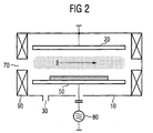
- the reactor exists essentially from a vacuum chamber 10 with an inlet 70 for the etching gas, a connection 30 for the vacuum pump and two parallel electrodes 20, 50.
- the semiconductor wafer to be etched is on one of the two electrodes, in the case shown on the lower electrode 50.
- the lower electrode 50 is also capacitively coupled to a high voltage 80.
- the upper electrode 20 is with the vacuum chamber 10 connected and grounded.
- the previously evacuated vacuum space 10 becomes suitable for the material to be etched via the inlet 70 Etching gas supplied.
- a substantially Etching gas mixture consisting of nitrogen and hydrogen is used.
- the etching gas mixture has reactive etching gases preferably at least 80% hydrogen and nitrogen.
- the ratio of hydrogen and nitrogen is preferably 1: 1.
- the etching gas mixture can also contain additives contain the etching gas properties in relation to the circumstances improve the dry etching method used in each case.
- the chemical-physical shown in the drawings Dry etching process in the form of reactive ion etching an etching gas mixture is used that, in addition to inevitable Impurities only from hydrogen and oxygen exists, each in equal proportions.
- the pressure range for etching the organic anti-reflection layer 3 is preferably in the range from 2.67 to 26.67 Pa (20 to 200 mTorr).
- the gas flow rate is preferably set to 0.17 to 1.67 10 -6 m 3 sec -1 (10 to 100 sccm).
- An applied high voltage causes the etching gas mixture between the electrodes 20, 50 to glow discharge.
- a low-pressure, low-temperature plasma with ions and electrons is created. Since the upper electrode 20 is connected to the vacuum chamber 10 and grounded, the upper electrode 20 has a larger surface area than the lower electrode 50. As a result, the lower electrode 50 charges more negatively than the upper electrode 20.
- the plasma On the way to the semiconductor wafer to be etched, the plasma thus receives sufficient kinetic energy to initiate a chemical reaction with the organic antireflection layer 3. In doing so, they arrive perpendicular to the surface to be etched and thus transfer the mask specified by the photoresist layer 4 to the organic antireflection layer , As shown in FIG. 2, the etching is preferably assisted by a magnetic field generated by magnets 90 in the vacuum chamber 10. The magnetic field compresses the plasma over the layer to be etched. This significantly increases the number of ions available for etching. A magnetic field up to 120 Gauss can be used.
- Etching the organic anti-reflective layer with an etching gas mixture of hydrogen and Nitrogen also ensures high-precision transmission the mask specified by the photoresist onto the one below Semiconductor layer.
- the etching is absolutely true to the profile steep paint flanks so that an anisotropy factor of essentially 1 is reached.
- losses of organic Anti-reflective layer when transferring the photoresist mask on the one under the organic anti-reflection layer Semiconductor layer reliably prevented, i.e. a high CD loyalty is achieved.
- the use of hydrogen-nitrogen chemistry also enables the etching of the semiconductor layer lying under the organic antireflection layer, in which the organic antireflection layer serves as a masking layer in one and the same etching reactor.
- the etching of the silicon dioxide layer, which is generally beneath the organic antireflection layer, is preferably also carried out by means of reactive-field-assisted reactive ion etching, a typical oxide etching process being carried out with the following process conditions.
- the pressure in the vacuum chamber is approx. 20 Pa (150 mTorr).
- CHF 3 and CF 4 are used as etching gases, the gas flow being 0.58 10 -6 m 3 sec -1 (35 sccm) and 0.42 10 -6 m 3 sec -1 (25 sccm). Furthermore, to improve the etching behavior, argon is fed in at a flow rate of 2.5 10 -6 m 3 sec -1 (approx. 150 sccm).
- the magnetic field to support the etching is preferably 15 gauss. Subsequent etching of an underlying oxide layer in the same etching chamber was not possible with the chemistry previously used as standard for etching the organic antireflection layer, since the chemistry for etching the organic antireflection layer was incompatible with the chemistry of the subsequent oxide etching.
- the use of hydrogen-nitrogen chemistry according to the invention which enables the etching chamber used for this purpose to be used for the subsequent oxide etching, achieves a substantial time and cost saving effect.
- 3 and 4 show electron micrographs of a lithography for structuring the first metallization level in an integrated semiconductor circuit with the conventional Chlorine-oxygen chemistry and with the hydrogen-nitrogen chemistry according to the invention.
- 3A is a cross section through a bilevel photoresist system on a silicon dioxide layer after opening the anti-reflective layer with the help conventional chlorine-oxygen chemistry.
- Figure 3B represents the same structure after opening with the invention Hydrogen-nitrogen chemistry. Like a comparison the figure shows occurs at the opening of the organic anti-reflection layer with the help of chlorine-oxygen chemistry slight etching of the silicon oxide layer.
- the hydrogen-nitrogen chemistry on the other hand is absolutely selective to the silicon oxide layer.
- the chlorine-oxygen etching a strong faceting of both the flanks of the photoresist as well as the organic anti-reflection layer
- the width of the etching profile also depends on the height is.
- 4A and 4B each show the opening of the anti-reflection layer etching to structure the first metallization level, the one used as the mask layer organic anti-reflection layer is already removed. If the hydrogen-nitrogen chemistry according to the invention, such as 4B to open the organic anti-reflection layer used results in the following Etching for structuring the metal layer clearly an improved Profile of the metal tracks.
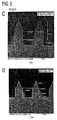
- Fig. 5 shows electron micrographs for opening the organic Antireflection layer in FIG. 5A before the Etching, in FIG. 5B after an etching time of 40 sec, in FIG. 5C after an etching time of 80 sec and in Fig. 5D after one Etching time of 120 sec.
- the vertical erosion of the top layer of photoresist with the Etching time increases, but the etching width is independent of the etching time remains constant, thus a perfect etching true to the CD is achieved.
- the flank shape of the Lacquer and the organic anti-reflection layer largely preserved, however, the height of the vertical side wall with time is decreasing.
Landscapes
- Drying Of Semiconductors (AREA)
- Surface Treatment Of Optical Elements (AREA)
Abstract
Description
- Fig. 1A-D
- schematische Darstellungen der Prozessschritte einer Lithographie mit einer organischer Antireflexionsschicht;
- Fig. 2
- den Aufbau eines Parallelplattenreaktors zum magnetfeldunterstützten reaktiven Ionenätzen;
- Fig. 3A/B
- Vergleichsaufnahmen einer Ätzung einer organischen Antireflexionsschicht mit einer Chlor-Sauerstoff-Chemie und der erfindungsgemäßen Wasserstoff-Stickstoff-Chemie;
- Fig. 4A/B
- Vergleichaufnahmen der Ätzung der ersten Metallebene nach dem Öffnen der organischen Antireflexionsschicht mit einer Chlor-Sauerstoff-Chemie bzw. der erfindungsgemäßen Wasserstoff-StickstoffChemie; und
- Fig. 5A-D
- Aufnahmen von der Ätzung einer organischen Antireflexionsschicht mit der erfindungsgemäßen Wasserstoff-Stickstoff-Chemie nach verschiedenen Ätzzeiten.
Claims (9)
- Verfahren zum anisotropen Trockenätzen einer organischen Antireflexionsschicht,
dadurch gekennzeichnet, dass
die Ätzgaszusammensetzung im Wesentlichen Wasserstoff und Stickstoff enthält. - Verfahren nach Anspruch 1, dadurch gekennzeichnet, dass Wasserstoff und Stickstoff im Verhältnis 1:1 verwendet werden.
- Verfahren nach Anspruch 1 oder 2, dadurch gekennzeichnet, dass die Ätzgaszusammensetzung als reaktive Ätzgase mindestens 80% Wasserstoff und Stickstoff enthält.
- Verfahren nach Anspruch 3, dadurch gekennzeichnet, dass die Ätzgaszusammensetzung als reaktive Ätzgase nur Wasserstoff und Stickstoff enthält.
- Verfahren nach einem der Ansprüche 1 bis 4, dadurch gekennzeichnet, dass die Ätzgaszusammensetzung Additive enthält, die Ätzgaseigenschaften in Bezug auf das verwendete Trockenätzverfahren verbessern.
- Verfahren nach einem der Ansprüche 1 bis 5, dadurch gekennzeichnet, dass eine Photolackschicht als Ätzmaske für die organische Antireflexionsschicht dient, wobei die Ätzgaszusammensetzung so eingestellt ist, dass der vertikale Äbbag des Photolacks maximal der Ätzrate der organischen Antireflexionsschicht entspricht.
- Verfahren nach einem der Ansprüche 1 bis 6, dadurch gekennzeichnet, dass folgende Prozeßparameter zum reaktiven Ionenätzen der organischen Antireflexionsschicht eingesetzt werden:Druck der Ätzgase im Bereich zwischen 2,67 bis 26,67 Pa (20 und 200 mTorr),Fluss der Ätzgase im Bereich zwischen 0,17 bis 1,67 10-6 m3sec-1 (10 und 100 sccm).
- Verfahren nach Anspruch 7, dadurch gekennzeichnet, dass ein magnetfeldunterstütztes reaktives Ionenätzen mit einer Feldstärke von 0 bis 120 Gauss eingesetzt wird.
- Verfahren nach einem der Ansprüche 1 bis 6, dadurch gekennzeichnet, dass zum Ätzen der organischen Antireflexionsschicht die Elektron-Zyklon-Resonanz-Plasmaquelle oder das induktiv gekoppelte Plasma oder die Helicon-Quelle eingesetzt wird.
Applications Claiming Priority (2)
| Application Number | Priority Date | Filing Date | Title |
|---|---|---|---|
| DE10037957A DE10037957C1 (de) | 2000-07-27 | 2000-07-27 | Verfahren zum anisotropen Trockenätzen organischer Antireflexionsschichten |
| DE10037957 | 2000-07-27 |
Publications (2)
| Publication Number | Publication Date |
|---|---|
| EP1176634A2 true EP1176634A2 (de) | 2002-01-30 |
| EP1176634A3 EP1176634A3 (de) | 2006-01-04 |
Family
ID=7651255
Family Applications (1)
| Application Number | Title | Priority Date | Filing Date |
|---|---|---|---|
| EP01115152A Withdrawn EP1176634A3 (de) | 2000-07-27 | 2001-06-22 | Verfahren zum anisotropen Trockenätzen von organischer Antireflexionsschichten |
Country Status (4)
| Country | Link |
|---|---|
| US (1) | US20020011462A1 (de) |
| EP (1) | EP1176634A3 (de) |
| DE (1) | DE10037957C1 (de) |
| TW (1) | TW555885B (de) |
Families Citing this family (10)
| Publication number | Priority date | Publication date | Assignee | Title |
|---|---|---|---|---|
| JP2003234331A (ja) * | 2001-12-05 | 2003-08-22 | Tokyo Electron Ltd | プラズマエッチング方法およびプラズマエッチング装置 |
| DE10241990B4 (de) * | 2002-09-11 | 2006-11-09 | Infineon Technologies Ag | Verfahren zur Strukturierung von Schichten auf Halbleiterbauelementen |
| JP4594235B2 (ja) * | 2002-12-23 | 2010-12-08 | 東京エレクトロン株式会社 | Arc層をエッチングする方法 |
| US7113717B2 (en) | 2004-03-30 | 2006-09-26 | Xerox Corporation | Closed loop control of nip pressure in a fuser system |
| WO2007024134A1 (en) * | 2005-08-26 | 2007-03-01 | Fujifilm Manufacturing Europe B.V. | Method and arrangement for generating and controlling a discharge plasma |
| JP2009538989A (ja) * | 2006-05-30 | 2009-11-12 | フジフィルム マニュファクチャリング ユーロプ ビー.ブイ. | パルス化大気圧グロー放電を使用する堆積の方法及び装置 |
| US8338307B2 (en) * | 2007-02-13 | 2012-12-25 | Fujifilm Manufacturing Europe B.V. | Substrate plasma treatment using magnetic mask device |
| WO2009096785A1 (en) * | 2008-02-01 | 2009-08-06 | Fujifilm Manufacturing Europe B.V. | Method and apparatus for plasma surface treatment of a moving substrate |
| US20100018944A1 (en) * | 2008-07-25 | 2010-01-28 | United Microelectronics Corp. | Patterning method |
| DE102009054630B4 (de) * | 2008-12-15 | 2013-02-14 | Qimonda Ag | Verfahren zum Herstellen eines photovoltaisches Bauelements |
Family Cites Families (6)
| Publication number | Priority date | Publication date | Assignee | Title |
|---|---|---|---|---|
| US4529860A (en) * | 1982-08-02 | 1985-07-16 | Motorola, Inc. | Plasma etching of organic materials |
| JPH08153704A (ja) * | 1994-11-28 | 1996-06-11 | Mitsubishi Electric Corp | 半導体装置の製造方法 |
| US5910453A (en) * | 1996-01-16 | 1999-06-08 | Advanced Micro Devices, Inc. | Deep UV anti-reflection coating etch |
| US6143476A (en) * | 1997-12-12 | 2000-11-07 | Applied Materials Inc | Method for high temperature etching of patterned layers using an organic mask stack |
| US5986344A (en) * | 1998-04-14 | 1999-11-16 | Advanced Micro Devices, Inc. | Anti-reflective coating layer for semiconductor device |
| US6114250A (en) * | 1998-08-17 | 2000-09-05 | Lam Research Corporation | Techniques for etching a low capacitance dielectric layer on a substrate |
-
2000
- 2000-07-27 DE DE10037957A patent/DE10037957C1/de not_active Expired - Fee Related
-
2001
- 2001-06-22 EP EP01115152A patent/EP1176634A3/de not_active Withdrawn
- 2001-07-25 TW TW090118145A patent/TW555885B/zh active
- 2001-07-27 US US09/917,549 patent/US20020011462A1/en not_active Abandoned
Also Published As
| Publication number | Publication date |
|---|---|
| EP1176634A3 (de) | 2006-01-04 |
| US20020011462A1 (en) | 2002-01-31 |
| DE10037957C1 (de) | 2002-02-28 |
| TW555885B (en) | 2003-10-01 |
Similar Documents
| Publication | Publication Date | Title |
|---|---|---|
| DE69718142T2 (de) | Verfahren zum ätzen von halbleiterscheiben | |
| DE2754396C2 (de) | ||
| DE69935100T2 (de) | Verfahren zur Ätzung einer Metallisierung mittels einer harten Maske | |
| EP0015403B1 (de) | Verfahren zum reaktiven Ionenätzen von Silicium | |
| DE102004043855B4 (de) | Verfahren zur Herstellung einer Magnet-Tunnel-Junction-Vorrichtung | |
| DE3856022T2 (de) | Selektives Ätzen dünner Schichten | |
| DE69126455T2 (de) | Verfahren zum Ätzen von Mehrschicht-Photolack mit geringer Unterätzeigenschaft und keiner Veränderung des Photolacks während des Ätzens | |
| DE3140890C2 (de) | Photolithographisches Verfahren zum Herstellen einer integrierten Schaltungsvorrichtung | |
| DE69228044T2 (de) | Verfahren zur Strukturierung von Wolframschichten | |
| DE69724192T2 (de) | Verfahren zum Ätzen von Polyzidstrukturen | |
| DE69513758T2 (de) | Ätzverfahren und Plasmareaktor zur Durchführung desselben | |
| DE4201661A1 (de) | Verfahren zur herstellung einer halbleiteranordnung | |
| DE4300983C2 (de) | Ätzverfahren für die Herstellung einer Halbleitervorrichtung | |
| EP0008359A2 (de) | Verfahren zum Herstellen einer Dünnfilmstruktur | |
| EP0002669B1 (de) | Verfahren zum Entfernen von Material von einem Substrat durch selektive Trockemätzung und Anwendung dieses Verfahrens bei der Herstellung von Leitungsmustern | |
| DE10051380C2 (de) | Verfahren zur Herstellung eines Halbleiterbauteils unter Anwendung eines Schrumpfprozesses eines Strukturmerkmals | |
| DE10252337A1 (de) | Verfahren zum Herstellen eines Halbleiterbauteils | |
| DE10037957C1 (de) | Verfahren zum anisotropen Trockenätzen organischer Antireflexionsschichten | |
| EP0013711A2 (de) | Verfahren zum Ätzen von Chrom | |
| EP0338102A1 (de) | Verfahren zur Herstellung von integrierten Halbleiterstrukturen welche Feldeffekttransistoren mit Kanallängen im Submikrometerbereich enthalten | |
| DE19903196A1 (de) | Verfahren zur Verbesserung der Erkennbarkeit von Alignmentmarken | |
| DE112007001243T5 (de) | Verfahren zum Trockenätzen einer Zwischenisolierschicht | |
| DE112006000811B4 (de) | Ätzprozess für CD-Reduzierung eines ARC-Materials | |
| DE10226603A1 (de) | Verfahren zum Strukturieren einer Siliziumschicht sowie dessen Verwendung zur Herstellung einer integrierten Halbleiterschaltung | |
| DE3219284C2 (de) |
Legal Events
| Date | Code | Title | Description |
|---|---|---|---|
| PUAI | Public reference made under article 153(3) epc to a published international application that has entered the european phase |
Free format text: ORIGINAL CODE: 0009012 |
|
| AK | Designated contracting states |
Kind code of ref document: A2 Designated state(s): AT BE CH CY DE DK ES FI FR GB GR IE IT LI LU MC NL PT SE TR |
|
| AX | Request for extension of the european patent |
Free format text: AL;LT;LV;MK;RO;SI |
|
| PUAL | Search report despatched |
Free format text: ORIGINAL CODE: 0009013 |
|
| AK | Designated contracting states |
Kind code of ref document: A3 Designated state(s): AT BE CH CY DE DK ES FI FR GB GR IE IT LI LU MC NL PT SE TR |
|
| AX | Request for extension of the european patent |
Extension state: AL LT LV MK RO SI |
|
| 17P | Request for examination filed |
Effective date: 20060131 |
|
| AKX | Designation fees paid |
Designated state(s): DE FR GB IE IT |
|
| STAA | Information on the status of an ep patent application or granted ep patent |
Free format text: STATUS: THE APPLICATION IS DEEMED TO BE WITHDRAWN |
|
| RAP1 | Party data changed (applicant data changed or rights of an application transferred) |
Owner name: INFINEON TECHNOLOGIES AG |
|
| 18D | Application deemed to be withdrawn |
Effective date: 20100105 |