EP1175774B1 - Schaltung zum verarbeiten eines zeitdiskreten analogsignals und bildsensor - Google Patents
Schaltung zum verarbeiten eines zeitdiskreten analogsignals und bildsensor Download PDFInfo
- Publication number
- EP1175774B1 EP1175774B1 EP00922578A EP00922578A EP1175774B1 EP 1175774 B1 EP1175774 B1 EP 1175774B1 EP 00922578 A EP00922578 A EP 00922578A EP 00922578 A EP00922578 A EP 00922578A EP 1175774 B1 EP1175774 B1 EP 1175774B1
- Authority
- EP
- European Patent Office
- Prior art keywords
- terminal
- node
- transistor
- circuit
- potential
- Prior art date
- Legal status (The legal status is an assumption and is not a legal conclusion. Google has not performed a legal analysis and makes no representation as to the accuracy of the status listed.)
- Expired - Lifetime
Links
Images

Classifications
-
- H—ELECTRICITY
- H03—ELECTRONIC CIRCUITRY
- H03F—AMPLIFIERS
- H03F3/00—Amplifiers with only discharge tubes or only semiconductor devices as amplifying elements
- H03F3/50—Amplifiers in which input is applied to, or output is derived from, an impedance common to input and output circuits of the amplifying element, e.g. cathode follower
-
- H—ELECTRICITY
- H03—ELECTRONIC CIRCUITRY
- H03F—AMPLIFIERS
- H03F3/00—Amplifiers with only discharge tubes or only semiconductor devices as amplifying elements
- H03F3/50—Amplifiers in which input is applied to, or output is derived from, an impedance common to input and output circuits of the amplifying element, e.g. cathode follower
- H03F3/505—Amplifiers in which input is applied to, or output is derived from, an impedance common to input and output circuits of the amplifying element, e.g. cathode follower with field-effect devices
-
- H—ELECTRICITY
- H03—ELECTRONIC CIRCUITRY
- H03F—AMPLIFIERS
- H03F3/00—Amplifiers with only discharge tubes or only semiconductor devices as amplifying elements
- H03F3/72—Gated amplifiers, i.e. amplifiers which are rendered operative or inoperative by means of a control signal
-
- H—ELECTRICITY
- H04—ELECTRIC COMMUNICATION TECHNIQUE
- H04N—PICTORIAL COMMUNICATION, e.g. TELEVISION
- H04N25/00—Circuitry of solid-state image sensors [SSIS]; Control thereof
-
- H—ELECTRICITY
- H04—ELECTRIC COMMUNICATION TECHNIQUE
- H04N—PICTORIAL COMMUNICATION, e.g. TELEVISION
- H04N25/00—Circuitry of solid-state image sensors [SSIS]; Control thereof
- H04N25/70—SSIS architectures; Circuits associated therewith
- H04N25/76—Addressed sensors, e.g. MOS or CMOS sensors
- H04N25/78—Readout circuits for addressed sensors, e.g. output amplifiers or A/D converters
-
- H—ELECTRICITY
- H03—ELECTRONIC CIRCUITRY
- H03F—AMPLIFIERS
- H03F2200/00—Indexing scheme relating to amplifiers
- H03F2200/417—A switch coupled in the output circuit of an amplifier being controlled by a circuit
-
- H—ELECTRICITY
- H03—ELECTRONIC CIRCUITRY
- H03F—AMPLIFIERS
- H03F2200/00—Indexing scheme relating to amplifiers
- H03F2200/75—Indexing scheme relating to amplifiers the amplifier stage being a common source configuration MOSFET
Definitions
- the present invention relates generally to the Processing of analogue signals and in particular to the Processing of time-discrete analog signals, as for example at the output of an image sensor with a plurality of pixel cells occur.
- Discrete-time analog signals are special analog signals, which in a certain interval is a substantially constant Have levels that theoretically directly to one other constant level in a next interval jumps.
- time-discrete analog signals with real Circuits that have inherent low-pass characteristics, be processed this leads to the theoretical infinitely steep flanks at the interval boundaries flatter and the time-discrete signal level of an interval not at the edge of the interval but only after a certain "settling time” sets. Only when the level has been set is the time-discrete analog signal meaningful, which is why this section of the interval as information-bearing section of the time-discrete analog signal referred to as.
- image sensors that are read serially deliver such a time-discrete analog signal.
- a Image sensor with a line of 512 pixels is considered so the 512 pixels are sequentially controlled by one Clock signal, read out, so that at the output of the image sensor a discrete-time analog signal results in his first interval, an illumination value of the first pixel represents and in its last interval an illumination value of the 512th pixel.
- a sensor could have multiple outputs, such that no full serial readout takes place, but a mixed serial / parallel readout.
- a Image sensor generally less analog outputs than pixels having. Therefore, the analog values must have several pixels by multiplexing with the highest possible rate be transmitted via the outputs of the image sensor.
- JP 62-220010 discloses a circuit for selective Reducing a base potential of a second transistor, its base with an output node of a first transistor connected is. Between the output node of the first Transistor and a ground potential is a Power source.
- the first transistor, called npn transistor is executed, is connected such that its emitter terminal is connected to the output node that its collector terminal connected to a battery voltage, and in that an input potential is applied to the base terminal of the npn transistor can be applied.
- JP-07245536-A discloses an amplifier circuit with an output control function, this circuit a inverted Darlington circuit used.
- the Darlington circuit consists of a first transistor and a second transistor, wherein the emitter terminal of the first Transistor via a switch with the collector terminal the second transistor is connected. Further, the collector terminal the first switch via a power supply connected, in turn, to the emitter terminal the second transistor is in communication.
- the input connection the circuit is connected through the base terminal of the first Transistor formed while the output terminal of the Circuit through the collector terminal of the second transistor is formed.
- Post-published EP 0952730 A2 discloses a solid-state imaging device, at the one pixel one Photodiode, a transfer switch, a reset switch, a pixel amplifier and a row selection switch.
- the row select switch turns the pixel amplifier connected to a node to intervene with one Source and ground lying current source as a source follower work. If the row selection switch is not open, so the pixel amplifier works in triode mode to be on its Gate capacitance as large a charge of the photodiode take.
- Between the source terminal of the pixel amplifier and a latch unit are transfer gates intended. Further, the source terminal of the pixel amplifier connected to ground via a reset switch. The reset switch and the transfer gates will be so switched, that the signal storage unit always from the Power source and the source terminal is disconnected when the Reset switch the source terminal and the power source with the circuit ground connects.
- the object of the present invention is to provide a Circuit for processing a time-discrete analog signal to create, despite low effort a high speed reached.
- Another object of the present invention is to create a fast image sensor.
- the present invention is based on the knowledge that for a quick settling of an amplifier stage on a certain voltage value in addition to the size of the load capacity and in addition to the transhipment of this load capacity for Available current and the starting value of the output voltage is crucial at the beginning of the transient process. Therefore, in order to obtain a fast amplifier stage According to the invention, the starting value of the output voltage at the beginning the transient manipulated to the time required by Amplifier stages for settling to an output voltage value to minimize with given accuracy.
- the Output node of the circuit according to the invention at an embodiment corresponds to the emitter or the source, preferably at the end and / or at the beginning of each interval, z.
- a reference node From the end of the preceding interval until to begin the following interval with a reference node connects to discharge the load capacity (npn emitter follower or n-channel source follower) or charge (pnp emitter follower or p-channel source follower) such that all transshipment of capacity due to time discrete Analog signal due to the previously described fast effect take place and no transhipment of the load capacity via a high-impedance resistor or via a high-impedance power source must take place.
- load capacity npn emitter follower or n-channel source follower
- charge pnp emitter follower or p-channel source follower
- the invention will be an npn emitter follower and an n-channel source follower, respectively used.
- the reference potential less than or equal to the smallest voltage level the time-discrete analog signal.
- the reference potential is greater or equal to the largest signal level of the analog signal.
- Invention is also a second switch between the collector or drain terminal of the respective transistor and a node to which a supply potential is applied, or between the emitter and source terminals and the other Node to which the other supply voltage potential is applied, provided, which is substantially synchronous is actuated to the first switch in order to in which the output is shorted to the reference potential is to "disconnect" the voltage supply of the transistor, high cross currents through the transistor during this time to reduce power dissipation.
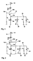
- Fig. 1 shows a circuit for processing an analogue signal U e which has a temporal sequence of discrete voltage levels and for purposes of the present invention is referred to as discrete-time analogue signal.
- the discrete-time analog signal comprises a plurality of time intervals, wherein each time interval is associated with a discrete signal level representing an information-bearing portion of the corresponding interval, while the remainder of the time interval is a non-information-bearing portion.
- the discrete-time analog signal U e is applied to an npn transistor (10) and in particular to a first gate (10a) of the transistor, which is the base terminal of the transistor (10).
- a second gate (10b) of the transistor, which is the collector terminal thereof, is connected to means (14) for applying a voltage supply U B via a switch (12) which will be discussed later.
- the expression "Gate” generally has an external access to a transistor should mean that with a voltage or a current can be applied.
- a voltage applied to the "basistor" of a transistor so means this is that an output of the voltage source to the base terminal the transistor is connected while the other Output of the voltage source with a reference node, such. B. the ground node, is connected.
- a power to the Basistor created it means that a connection of a Current source connected to the base terminal of the transistor while the other connection of the power source with a any reference node, z. B. mass, is connected.
- a load current source I DC (20) which is a DC source and the operating point of the Transistor (10) defined.
- I DC (20) which is a DC source and the operating point of the Transistor (10) defined.
- an emitter resistor could be provided instead of the load current source (20). Both the load current source (20) and the emitter resistor can be considered as means for supplying a direct current between the emitter terminal (10c) of the transistor (10) and the ground node (18). If a constant current source is used instead of a high-resistance emitter resistor, the high voltage drop across the emitter resistor can be avoided, as is known to those skilled in the art.
- An output node 19 of the circuit shown in Fig. 1 forms the emitter terminal (10c) of the transistor (10) together with the second node (18), wherein between these two nodes an output voltage U a is applied.
- the output voltage U a of the input voltage U e follows, wherein the amount of the output voltage U a is approximately the amount of the input voltage U e less about 0.6 V.
- this circuit is also referred to as emitter follower.
- the emitter follower may also be considered as an impedance converter, which allows a high-impedance stage to be coupled to a low-resistance stage without loss of voltage.
- the output node 19 of an amplifier stage is capacitively loaded, which is shown in FIG. 1 and also in FIGS. 2 to 4 as a load capacitance C L.
- This load capacitance C L (22) can be composed on the one hand of a capacitive impedance of a subsequent circuit or on the other hand of line capacitances or parasitic capacitances between the output and ground.
- this load capacitance C L (22) is treated as a lumped element in the figures.
- a first switch (24) provided to the third Gate (10c), d. H. the emitter terminal with a reference potential (26) to short circuit, which in Fig. 1 identical to the ground potential (18).
- the reference potential (26) could also, for example, a low-impedance Source for discharging the load capacity (22), for example in the form of a power supply or a charged Be capacity.
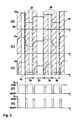
- the partial image 5 (a) of FIG. 5 represents a time-discrete analog signal U e over the time t, which is obtained, for example, when an image sensor is read out ideally, ie without the low-pass effect always present in real circuits.
- the sub-image 5 (b) shows the same time-discrete analog signal as in the sub-image 5 (a), which has already been subjected to a low-pass effect inherent in real circuits, for which reason the transitions from one interval to the next are no longer infinitely steep, but one have a certain flatter or curved course.
- the partial image 5 (a) 5 (b) and 5 (c) show hatched areas (38) representing the non-information bearing portions of the waveform, and it can be seen that they are arranged around the interval boundaries, which are known to be known in advance occurring voltage values are indeterminate, since they are subjected to a transient response, as shown for example in the field 5 (b) for the input voltage U e .
- the areas 38 extend not only from an interval boundary to the right, but also from an interval boundary to the left, such that the information-bearing, non-hatched portions remain, which are characterized in that in them the respective signal level of the time-discrete analog signal is substantially constant. Only the information-carrying sections of the intervals 30, 32, 34, 36 are important for an information evaluation, but not the non-information-bearing hatched sections 38 and the hatched portion of an interval preceding the interval 30.
- the left edge of the interval 30 is considered.
- Left of the left edge of the interval 30 is the input signal U e and therefore also the output signal U a at a high level.
- the input signal U e then assumes a low level in the interval 30, which should also take the output signal U a as quickly as possible.
- the load capacitance C L 22 must be discharged to the low level of the output signal U a in the interval 30. From Fig. 1 it can be seen that this discharge is possible only via the high-impedance load current source 20 and an alternative existing high-resistance emitter resistor. The discharge would therefore take place very slowly, which significantly affects the speed of the emitter follower stages according to the prior art.
- the switch 24 is now short-circuited in the non-information-bearing portion of the interval 30, such that the charge of the load capacitor 22, which is proportional to the applied voltage U a from the interval before the interval 30, can flow to the reference potential 26.
- This discharge takes place very rapidly, since a "short circuit" connection which is low in comparison to the load current source is produced by the switch 24.
- the term "short circuit” is not to be understood as having a resistance of 0 ohms. If the switch is realized as a transistor, it could well have an on-resistance in the range of a few hundred ohms when closed. However, this value is small in comparison to the resistance of the current source or to a very high-impedance emitter resistor and can therefore be referred to for the sake of clarity as a "short circuit".
- This charge is dynamically amplified because the transistor 10 is turned on. If the simple case is considered that the output voltage U a is discharged by the operation of the switch 24 to ground and a certain input voltage U e is applied, this results in that the emitter voltage is initially at 0 volts, which is why a large base Emitter voltage is applied and the transistor allows a large current flow from the collector terminal 10 b to the emitter terminal 10 c, which charges the capacitor C L 22. With increasing output voltage U a , the transistor 10 is increasingly blocked because the base-emitter voltage continues to decrease until the transistor has again reached the operating point defined by the current source. Due to the dynamic effect, however, it has been achieved that the capacitor C L 22 is charged faster than is possible by the constant current source 20 alone.
- the charging of the load capacitance 22 is a fast process due to the dynamic current increase.
- the capacitor C L is again discharged by briefly closing the switch 24, in order then to be charged to the level which is provided for the information-carrying part of the interval 32.
- the capacitor 22 is discharged again, in order then to be recharged after opening the switch 24 to the information-carrying value of the interval 34.
- the capacitor in a non-information carrying section is always set to a start value at the beginning of each interval, which ensures that charging of the capacitor C L to the corresponding discrete signal level occurs at substantially every interval.
- ⁇ 1 For the control signal of the switch 24, which is referred to as ⁇ 1 , results in a course, as shown in part 5 (e).
- the second switch 12 is controlled by a signal referred to as ⁇ 2 and in figure 5 (d).
- ⁇ 2 and in figure 5 (d) In order to ensure that the switch 12 is opened in any case when the switch 24 is closed, it is preferred that the opening time of the switch 12 is slightly greater than the closing time of the switch 24.
- the two control signals ⁇ 1 and ⁇ 2 for the Both switches 24 and 12 therefore do not have to be completely complementary to one another.
- the reference potential at the reference node 26 is equal to the ground potential at the ground node 18 shown.
- the reference node 26 could also be a low-resistance voltage source or a capacitor charged to the reference potential, such that the capacitor C L 22 is not discharged exactly to 0 V, ie ground, in each interval, but only on a value less than the lowest value that is expected to occur in the discrete-time analog signal.
- a circuit such as shown in FIG. 1 could have a battery voltage U B that produces a +5 V potential to ground.
- the discrete voltage levels may be such that they are never less than z. B. 1 V are.
- the low-resistance power source defining the reference potential in this case would be a voltage source set to 1V. This ensures that the output capacitor C L 22 will not discharge too much to still take up more time than necessary for subsequent charging, although it proceeds quickly. Another point is that an amplifier stage fed, for example, with the output signal U a is not driven into saturation by the strong wastes present in the output signal U a and subsequent charging processes (reference numeral 40 in FIG. 5).
- the reference potential can also be selected to be a discharge to reach a voltage level between the highest and lowest expected discrete signal levels the discrete-time analog signal, for example a lot of high discrete signal levels expected and only a few are low. In this case could There is already a speed advantage, since the vast majority of signal levels are reached very quickly while only a few are reached very slowly. Therefore, it can be seen that the reference potential in certain Borders can be varied, not least of all depend on the time-discrete analog signal to be processed. So it represents only a preferred embodiment of the present invention, the reference potential is smaller or equal to the lowest expected discrete level to select the time-discrete analog signal.
- Another possibility is to operate the switch 24 only so short that the capacitor can not fully discharge to the actual potential applied to the reference node 26, whereby the reference potential, after reopening the switch 24 to the emitter 10c of the Transistor 10 is applied, does not correspond to the potential at the reference node 26 but is correspondingly larger. Also in this case, the load capacitor C L 22 is discharged, but not exactly to the potential at the reference node 26 but to a depending on the closing duration of the switch 24 correspondingly higher potential.
- switch 12 between the node 16 and the Collector terminal 10b could be the same between the emitter terminal 10c and the output node 19 are provided be, so also to the DC path through the Transistor to break when the switch 24 is closed is, so that the power loss can be kept low.
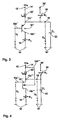
- Fig. 2 is a Circuit according to a second embodiment of the present Invention shows.
- Fig. 2 and the others Figures should be noted that parts with the same reference numerals are essentially identical and therefore, so they already described, not described again become.
- the field effect transistor 10' in FIG. 2 is drawn as a self-locking type. Alternatively could however, also a normally-on type or a junction FET be used.
- the bipolar transistor is drawn as emitter follower is the illustrated in Fig. 2 field effect transistor 10 'in Source follower configuration shown. It also includes a bulk port 10d ', in the usual way with the Ground potential 18 is connected.
- the operation of the n-channel source follower circuit of Fig. 2 is related to the Fig. 1 described analog manner.
- Fig. 3 shows a circuit according to a third embodiment of the present invention, which is complementary to the circuit shown in Fig. 1 according to the first embodiment of the present invention, such that instead of the npn bipolar transistor, a pnp bipolar transistor 10 '' is used ,
- the emitter 10b '' is now not connected to ground but via the constant current source I DC 20 'to the power supply potential U B.
- the collector of the pnp transistor 10 ", ie the gate 10c” is now connected to the ground potential via the switch 12.
- the capacitor 24 is not discharged to ground as in FIG.
- reference potential 26 ' This reference potential could be equal to the power supply potential or could be a potential that is greater than or equal to the highest expected discrete signal level of the time discrete analog signal.
- the reference potential 26 'could also be less than the highest expected value, if in analogy to the previously described only a few large discrete signal levels occur, such that only a short and rare long charge of the load capacitor C L 22 is accepted to limit the amount of charge that must be discharged mostly for smaller discrete signal levels. This, as previously described, has the effect that subsequent amplifier stages, ie amplifier stages which are switched in parallel with the load capacitance C L 22, are not loaded with high peaks and may thereby be driven into saturation.
- the reference potential 26 'could be provided either by a reference voltage source that provides the desired voltage for the reference potential, or by a capacitor charged to such a voltage value, the better the higher the capacitance of such a capacitor over the load capacitance C L 22 , Alternatively, the reference potential 26 'can also be controlled by the on-time of the switch 24, such that the switch 24 is closed only very briefly, whereby the potential to which the positive electrode of the capacitor C L 22 to a smaller potential than at the reference node is charged. In this case, the potential at the reference node should be chosen such that a desired reference potential is obtained, which is, for example, greater than or equal to the highest expected discrete signal level.
- the switch 24 thus enables the capacitance C L 22 to be charged very quickly to the reference potential, since the current is supplied to the capacitor C L 22 for low-impedance transfer. Thus, a slow charging via the load current source 20 'or alternatively via a high-impedance emitter resistor is avoided. On the other hand, a discharge of the capacitance C L 22 via the transistor 10 '' will happen very quickly and even dynamically amplified, since the transistor 10 '' is "turned on" when the input voltage U e is smaller than the output voltage U a . This is the case, since the difference between U e and U a directly applied as the base-emitter voltage of the transistor 10 ''.
- Fig. 4 shows a circuit according to a fourth embodiment of the present invention, which is identical to the circuit of Fig. 3 with the difference that instead of the pnp bipolar transistor 10 '' a p-channel field effect transistor 10 '''is present , whose bulk terminal bd '''is connected to the power supply potential U B , as is common in the art. Depending on the technology, the bulk potential can also be connected to the source terminal. Although a self-locking field-effect transistor is used in FIG. 4, a self-conducting type or a junction FET could be used analogously thereto.
- switches 12, 24 so far generally as Switches have been described, it should be noted that they are preferably realized as transistors be, these transistors in the same technology as the transistors of the follower stages are executed.
- the transistor type is arbitrary.
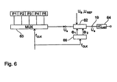
- Fig. 6 shows an application of the circuit according to the invention, which has been described with reference to Figs. 1 to 5, in an image sensor.
- the image sensor, the z. B. may be a line sensor for a line scan camera comprises a plurality of pixel elements P1 to P5.
- P1 to P5 pixel elements
- FIG. 6 shows only five pixel elements are drawn in FIG. 6 for the sake of illustration, it goes without saying that the number of pixel elements in a real application is arbitrary and depends on the implementation. For example, 512 or 1024 pixel elements can be used with a line scan camera. Alternatively, an array consisting of a plurality of pixel rows may also be used.
- the number of output lines will be smaller than the number of pixel elements, and therefore the output signals of the individual pixel elements are parallel / serial-converted via a multiplexer 60 to be output on an output line of the multiplexer.
- the output line of the multiplexer 60 is then applied to the discrete-time analog signal, which is the input signal U e for the circuit 62 for rapidly processing an analog signal, which is only generally shown in Fig. 6 and with reference to Figs. 1 to 4 explained in detail has been.
- any load capacitance will be present at the output of the circuit 62, be it that this load capacitance is the input capacitance of a subsequent amplifier stage, or represents the capacitance of the transmission lines present at the output of the circuit 62 or also comprises parasitic capacitances.
- the speed with which the discrete-time analog signals can be output is therefore substantially influenced by a capacitive loading of the output of the circuit 62.
- the read-out frequency f CLK must be selected to be very high.
- the circuit 62 comprises an input for the power supply potential U B and for the reference node or the reference potential U REF and is further connected to a timer 66 which consists of the clock signal with the frequency f CLK clock signals ⁇ 1 and ⁇ 2 for controlling the switch 24th and 12 ( Figure 1).
- Fig. 7 shows a detailed block diagram for a preferred one Embodiment of an image sensor of Fig. 6.
- the circuit 62 according to the invention is so separated, that part 62a thereof, i. H. the voltage source 14 and the transistor 10 '(FIG. 2), "multiplexed" on the individual ones Pixel sits while the other part 62b, d. H. the Current source 20, the load capacity 22 and the switch 24th (Fig. 1), is present only once.
- the alternative is used, in which the Switch 12, which is used to interrupt the DC path serve the transistor when the switch 24 is closed, to keep power consumption low.
- these can Switch which in Fig. 7 also with SEL1, SEL2, ..., SELN are designated to be used simultaneously for multiplexing, what should be indicated by the reference numeral 60. If the pixel with the number 1 is read, then during the selector switch SEL1 be closed while the other SELn switches and the switch 24 are open. Then, the switch SEL1 is opened to be in a non-informational part of the switch 24 to close to the effect of resetting according to the invention to reach a reference potential. After that then, only to read out the second pixel with the # 2 the switch SEL2 closed, etc.
- the switches meet 12 on the one hand, the dual function of multiplexing and on the other hand, interrupting the DC path through the Transistors when the switch 24 is closed.
Landscapes
- Engineering & Computer Science (AREA)
- Power Engineering (AREA)
- Multimedia (AREA)
- Signal Processing (AREA)
- Transforming Light Signals Into Electric Signals (AREA)
- Amplifiers (AREA)
- Inspection Of Paper Currency And Valuable Securities (AREA)
- Solid State Image Pick-Up Elements (AREA)
- Studio Devices (AREA)
- Color Television Image Signal Generators (AREA)
- Computer Vision & Pattern Recognition (AREA)
- Facsimile Heads (AREA)
Description
- Fig. 1
- eine Schaltung gemäß einem ersten Ausführungsbeispiel der vorliegenden Erfindung, die als npn-Emitterfolger ausgeführt ist;
- Fig. 2
- eine Schaltung gemäß einem zweiten Ausführungsbeispiel der vorliegenden Erfindung, die als n-Kanal-Sourcefolger ausgeführt ist;
- Fig. 3
- eine Schaltung gemäß einem dritten Ausführungsbeispiel der vorliegenden Erfindung, die als pnp-Emitterfolger ausgeführt ist;
- Fig. 4
- eine Schaltung gemäß einem vierten Ausführungsbeispiel der vorliegenden Erfindung, die als p-Kanal-Sourcefolger ausgeführt ist;
- Fig. 5
- ein Zeitdiagramm von Signalen, wie sie bei der in Fig. 1 gezeigten Schaltung auftreten;
- Fig. 6
- ein prinzipielles Blockdiagramm eines erfindungsgemäßen Bildsensors mit schneller Analogsignalverarbeitung; und
- Fig. 7
- ein detailliertes Blockdiagramm für ein bevorzugtes Ausführungsbeispiel eines Bildsensors von Fig. 6.
Claims (18)
- Schaltung zum Verarbeiten eines Analogsignals, das eine zeitliche Folge von diskreten Signalpegeln aufweist, wobei jeder diskrete Signalpegel in einem zeitlichen Intervall (30 - 36) liegt und einen informationstragenden Abschnitt des Intervalls darstellt, während der Rest (38) des Intervalls ein nicht-informationstragender Abschnitt ist, mit folgenden Merkmalen:einem Transistor (10; 10'; 10''; 10''') mit einem ersten (10a; 10a'; 10a''; 10a'''), einem zweiten (10b; 10b'; 10b''; 10b''') und einem dritten Anschluß (10c; 10c'; 10c''; 10c'''), wobei der Transistor derart angeordnet ist, daß durch ein Signal an dem ersten Anschluß ein Stromfluß zwischen dem zweiten und dem dritten Anschluß steuerbar ist, daß das zeitdiskrete Analogsignal (Ue) an den ersten Anschluß anlegbar ist, und daß der dritte Anschluß mit einem Ausgangsknoten (19) der Schaltung koppelbar ist;einer Einrichtung (14) zum Anlegen einer Spannung zwischen einem ersten Knoten (16; 16') mit einem ersten Potential (DB; 0V) und einem zweiten Knoten (18; 18') mit einem zweiten Potential (0 V; UB), wobei der erste Knoten (16) mit dem zweiten Anschluß des Transistors koppelbar ist;einer Einrichtung (20; 20') zum Liefern eines Gleichstroms (IDC) zwischen zwei Anschlüssen, wobei ein Anschluß mit dem Ausgangsknoten (19) und der andere Anschluß mit dem zweiten Knoten (18; 18') verbunden ist;einem ersten Schalter (24), der normalerweise geöffnet ist, und der steuerbar ist (Φ1), um in einem geschlossenen Zustand den Ausgangsknoten (19) zumindest einen Teil des nicht-informationstragenden Abschnitts (38) des Intervalls (30, 32, 34, 36) mit einem Referenzknoten (26; 26') zu verbinden, um ein Referenzpotential am Ausgangsknoten (19) der Schaltung zu erzeugen; undeinem zweiten Schalter (12), der zwischen den zweiten Anschluß des Transistors (10; 10'; 10''; 10''') und den ersten Knoten (16; 16') geschaltet ist, und der steuerbar ist, um eine elektrisch leitfähige Verbindung zwischen dem ersten Knoten (16; 16') und dem zweiten AnSchluß (10b; 10b'; 10b''; 10b''') des Transistors (10; 10'; 10''; 10''') zumindest solange zu unterbrechen, wie der erste Schalter (24) den dritten Anschluß (10c; 10c'; 10c''; 10c''') des Transistors mit dem Referenzknoten (26; 26') verbindet.
- Schaltung zum Verarbeiten eines Analogsignals, das eine zeitliche Folge von diskreten Signalpegeln aufweist, wobei jeder diskrete Signalpegel in einem zeitlichen Intervall (30 - 36) liegt und einen informationstragenden Abschnitt des Intervalls darstellt, während der Rest (38) des Intervalls ein nicht-informationstragender Abschnitt ist, mit folgenden Merkmalen:wobei der zweite Schalter (12) steuerbar ist, um eine elektrisch leitfähige Verbindung zwischen dem Ausgangsknoten (19) und dem dritten Anschluß des Transistors zumindest solange zu unterbrechen, wie der erste Schalter (24) den Ausgangsknoten mit dem zweiten Knoten verbindet.einem Transistor (10; 10'; 10''; 10''') mit einem ersten (10a; 10a'; 10a''; 10a'''), einem zweiten (10b; 10b'; 10b''; 10b''') und einem dritten Anschluß (10c; 10c'; 10c''; 10c'''), wobei der Transistor derart angeordnet ist, daß durch ein Signal an dem ersten Anschluß ein Stromfluß zwischen dem zweiten und dem dritten Anschluß steuerbar ist, daß das zeitdiskrete Analogsignal (Ue) an den ersten Anschluß anlegbar ist, und daß der dritte Anschluß mit einem Ausgangsknoten (19) der Schaltung koppelbar ist;einer Einrichtung (14) zum Anlegen einer Spannung zwischen einem ersten Knoten (16; 16') mit einem ersten Potential (UB; 0V) und einem zweiten Knoten (18; 18') mit einem zweiten Potential (0 V; UB), wobei der erste Knoten (16) mit dem zweiten Anschluß des Transistors koppelbar ist;einer Einrichtung (20; 20') zum Liefern eines Gleichstroms (IDC) zwischen zwei Anschlüssen, wobei ein Anschluß mit dem Ausgangsknoten (19) und der andere Anschluß mit dem zweiten Knoten (18; 18') verbunden ist;einem ersten Schalter (24), der normalerweise geöffnet ist, und der steuerbar ist (Φ1), um in einem geschlossenen Zustand den Ausgangsknoten (19) zumindest einen Teil des nicht-informationstragenden Abschnitts (38) des Intervalls (30, 32, 34, 36) mit einem Referenzknoten (26; 26') zu verbinden, um ein Referenzpotential am Ausgangsknoten (19) der Schaltung zu erzeugen; undeinem zweiten Schalter (12), der zwischen den dritten Anschluß (10c; 10c'; 10c''; 10c''') des Transistors und den Ausgangsknoten (19) der Schaltung geschaltet ist,
- Schaltung nach einem der vorhergehenden Ansprüche, bei der der Referenzknoten (26; 26') mit dem zweiten Knoten (18; 18') elektrisch leitfähig verbunden ist, derart, daß das Potential an dem Referenzknoten (26; 26') gleich dem Potential (0 V; UB) an dem zweiten Knoten (18; 18') ist.
- Schaltung nach Anspruch 1 oder 2, bei der der Referenzknoten (26; 26') ein Anschluß eines Kondensators ist, der aufgeladen ist, um das Referenzpotential zu erzeugen.
- Schaltung nach Anspruch 1 oder 2, bei der der Referenzknoten (26; 26') ein Anschluß einer Spannungsversorgung ist, die sich von einer Spannungsversorgung unterscheidet, die mit der Einrichtung (14) zum Anlegen einer Spannung verbindbar ist.
- Schaltung nach einem der vorhergehenden Ansprüche, bei der die Intervalle des Analogsignals (30, 32, 34, 36) eine konstante Länge aufweisen, die eine Taktfrequenz (fCLK) eines Taktsignals definiert, und bei der der erste Schalter durch ein Steuert (Φ1) steuerbar ist, das von dem Taktsignal abgeleitet ist.
- Schaltung nach einem der vorhergehenden Ansprüche, bei der die Einrichtung (20; 20') zum Liefern eines Gleichstroms (IDC) eine Konstantstromquelle mit hohem Innenwiderstand oder ein hochohmiger ohmscher Widerstand ist..
- Schaltung nach einem der vorhergehenden Ansprüche,
bei der der Transistor (10) ein npn-Transistor ist, wobei der erste Anschluß (10a) ein Basisanschluß ist, der zweite Anschluß (10b) ein Kollektoranschluß ist und der dritte Anschluß (10c) ein Emitteranschluß ist, und
bei der die Einrichtung (14) zum Anlegen einer Spannung angeordnet ist, um an dem ersten Knoten (16) ein positives Potential (UB) und an dem zweiten Knoten (18) ein Massepotential (0 V) zu erzeugen. - Schaltung nach einem der Ansprüche 1 bis 8,
bei der der Transistor (10') ein n-Kanal-FET ist, wobei der erste Anschluß (10a') ein Gate-Anschluß des Transistors ist, der zweite Anschluß (10b') ein Drain-Anschluß des Transistors ist und der dritte Anschluß (10c') ein Source-Anschluß des Transistors ist, und
bei der die Einrichtung (14) zum Anlegen einer Spannung angeordnet ist, um an dem ersten Knoten (16) ein positives Potential (UB) und an dem zweiten Knoten (18) ein Massepotential (0 V) zu erzeugen. - Schaltung nach Anspruch 8 oder 9, bei der der erste Schalter (24) angeordnet ist, um zumindest so lange geschlossen zu sein, bis das Potential an dem Ausgangsknoten (19) kleiner oder gleich einem kleinsten zu erwartenden diskreten Signalpegel des Analogsignals ist.
- Schaltung nach Anspruch 8 oder 9,
bei der das Potential an dem Referenzknoten (26) kleiner oder gleich dem niedrigsten zu erwartenden diskreten Signalpegel des Analogsignals ist, und
bei der der Schalter (24) angeordnet ist, um solange geschlossen zu sein, bis das Potential an dem Ausgangsknoten als Referenzpotential das Potential des Referenzknotens (26) hat. - Schaltung nach einem der Ansprüche 1 bis 7,
bei der der Transistor ein pnp-Transistor (10'') ist, wobei der erste Anschluß (10a'') eine Basis des Transistors ist, der zweite Anschluß (10b'') ein Kollektor des Transistors ist und der dritte Anschluß (10c'') ein Emitter des Transistors ist, und
bei der die Einrichtung (14) zum Anlegen einer Spannung angeordnet ist, um an dem ersten Knoten (16') ein Massepotential (0 V) und an dem zweiten Knoten (18') ein positives Spannungsversorgungspotential (UB) zu erzeugen. - Schaltung nach einem der Ansprüche 1 bis 7,
bei der der Transistor ein p-Kanal-FET (10''') ist, wobei der erste Anschluß (10a''') ein Gate-Anschluß des Transistors ist, der zweite Anschluß (10b''') ein Drain-Anschluß des Transistors ist und der dritte Anschluß (10c''') ein Source-Anschluß des Transistors ist, und
bei der die Einrichtung (14) zum Anlegen einer Spannung angeordnet ist, um an dem ersten Knoten (16') ein Massepotential (0 V) und an dem zweiten Knoten (18') ein positives Spannungsversorgungspotential (UB) zu erzeugen. - Schaltung nach Anspruch 12 oder 13, bei der der erste Schalter (24) angeordnet ist, um zumindest solange geschlossen zu sein, bis das Potential an dem Ausgangsknoten (19) größer oder gleich dem größten zu erwartenden diskreten Signalpegel ist.
- Schaltung nach Anspruch 12 oder 13,
bei der ein an den Referenzknoten (26') anlegbares Signal größer oder gleich dem größten zu erwartenden diskreten Signalpegel des Analogsignals ist, und
bei der der erste Schalter (24) angeordnet ist, um solange geschlossen zu sein, bis das Referenzpotential an dem Ausgangsknoten (19) der Schaltung das erwünschte Potential ist. - Schaltung nach einem der vorhergehenden Ansprüche, die ferner eine Kapazität (CL) zwischen dem Ausgangsknoten (19) der Schaltung und dem zweiten Knoten aufweist.
- Bildsensor mit einer Mehrzahl von Pixelelementen (P1 bis P5), mit folgenden Merkmalen:einer Einrichtung (60) zum seriellen Auslesen der Mehrzahl von Pixelelementen (P1 bis P5), um ein Analogsignal (Ue) zu liefern, das eine zeitliche Folge von diskreten Signalpegeln aufweist;einer Schaltung (62) zum Verarbeiten des Analogsignals nach einem der Ansprüche 1 bis 15, um ein Ausgangssignal (Ua) zu liefern, das dem Eingangssignal (Ue) entspricht; undeiner Kapazität (64), die parallel zu einem Ausgang der Schaltung (62) angeordnet ist.
- Bildsensor, mit folgenden Merkmalen:einer Mehrzahl von Pixelelementen (P1 bis PN) wobei jedes Pixelelement folgende Merkmale aufweist:einen Transistor (10; 10'; 10''; 10''') mit einem ersten (10a; 10a'; 10a''; 10a'''), einem zweiten (10b; 10b'; 10b''; 10b''') und einem dritten Anschluß (10c; 10c'; 10c''; 10c'''), wobei der Transistor derart angeordnet ist, daß durch ein Signal an dem ersten Anschluß ein Stromfluß zwischen dem zweiten und dem dritten Anschluß steuerbar ist, daß ein Pixelsignal (Ue1, Ue2, ..., UeN) an den ersten Anschluß anlegbar ist, und daß der dritte Anschluß mit einem Ausgangsknoten (19) des Bildsensors koppelbar ist;eine Einrichtung (14) zum Anlegen einer Spannung zwischen einem ersten Knoten (16; 16') mit einem ersten Potential (UB; 0V) und einem zweiten Knoten (18; 18') mit einem zweiten Potential (0 V; UB), wobei der erste Knoten (16) mit dem zweiten Anschluß des Transistors koppelbar ist; undeinen zweiten Schalter (SEL1, SEL2, ..., SELN) mit einem ersten und einem zweiten Anschluß, wobei der erste Anschluß des zweiten Schalters mit dem dritten Anschluß (10c; 10c'; 10c''; 10c''') des Transistors verbunden ist, und wobei der zweite Schalter (12) steuerbar ist, um seinen zweiten Anschluß mit dem dritten Anschluß des Transistors zu koppeln;einer gemeinsamen Ausgangsleitung für die Mehrzahl von Pixelelementen, die mit dem Ausgangsknoten (19) des Bildsensors und den zweiten Anschlüssen der zweiten Schalter (SEL1, SEL2, ..., SELN) der Pixelelemente verbunden ist;einer Einrichtung (20; 20') zum Liefern eines Gleichstroms (IDC) zwischen zwei Anschlüssen, wobei ein Anschluß mit der Ausgangsleitung und der andere Anschluß mit dem zweiten Knoten (18; 18') verbunden ist;einem ersten Schalter (24), der normalerweise geöffnet ist, und der steuerbar ist (Φ1), um in einem geschlossenen Zustand die gemeinsame Ausgangsleitung zumindest einen Teil eines nicht-informationstragenden Abschnitts (38) eines Pixelsignals (Ue1, Ue2, ..., UeN) mit einem Referenzknoten (26; 26') zu verbinden, um ein Referenzpotential am Ausgangsknoten (19) des Bildsensors zu erzeugen; undeiner Einrichtung (60) zum seriellen Auslesen der Mehrzahl von Pixelementen durch Steuern der zweiten Schalter (SEL1, SEL2, SELN), die angeordnet ist, um zum Liefern des Pixelsignals (Ue1) eines Pixelelements (SEL1) zum Ausgangsknoten (19) nur den zweiten Schalter (SEL1) dieses Pixelelements (PIXEL 1) zu schließen, während die zweiten Schalter (SEL2, ..., SELN) der anderen Pixelelemente (PIXEL 2, ..., PIXEL N) offen sind.
Applications Claiming Priority (3)
| Application Number | Priority Date | Filing Date | Title |
|---|---|---|---|
| DE19917863A DE19917863C1 (de) | 1999-04-20 | 1999-04-20 | Schaltung zum Verarbeiten eines Analogsignals und Bildsensor |
| DE19917863 | 1999-04-20 | ||
| PCT/EP2000/002834 WO2000064142A1 (de) | 1999-04-20 | 2000-03-30 | Schaltung zum verarbeiten eines zeitdiskreten analogsignals und bildsensor |
Publications (2)
| Publication Number | Publication Date |
|---|---|
| EP1175774A1 EP1175774A1 (de) | 2002-01-30 |
| EP1175774B1 true EP1175774B1 (de) | 2003-05-21 |
Family
ID=7905220
Family Applications (1)
| Application Number | Title | Priority Date | Filing Date |
|---|---|---|---|
| EP00922578A Expired - Lifetime EP1175774B1 (de) | 1999-04-20 | 2000-03-30 | Schaltung zum verarbeiten eines zeitdiskreten analogsignals und bildsensor |
Country Status (9)
| Country | Link |
|---|---|
| US (3) | US7295236B1 (de) |
| EP (1) | EP1175774B1 (de) |
| AT (1) | ATE241242T1 (de) |
| DE (2) | DE19917863C1 (de) |
| DK (1) | DK1175774T3 (de) |
| ES (1) | ES2195885T3 (de) |
| IL (2) | IL146014A0 (de) |
| PT (1) | PT1175774E (de) |
| WO (1) | WO2000064142A1 (de) |
Families Citing this family (8)
| Publication number | Priority date | Publication date | Assignee | Title |
|---|---|---|---|---|
| JP2001298663A (ja) * | 2000-04-12 | 2001-10-26 | Semiconductor Energy Lab Co Ltd | 半導体装置およびその駆動方法 |
| JP4654866B2 (ja) * | 2005-03-30 | 2011-03-23 | ソニー株式会社 | 容量性インピーダンスを持つ素子を駆動する駆動方法および駆動装置並びに撮像装置 |
| US20130127515A1 (en) * | 2011-11-22 | 2013-05-23 | Taiwan Semiconductor Manufacturing Company, Ltd. | Voltage dividing circuit |
| US8618865B1 (en) | 2012-11-02 | 2013-12-31 | Palo Alto Research Center Incorporated | Capacitive imaging device with active pixels |
| US10101373B2 (en) * | 2014-04-21 | 2018-10-16 | Palo Alto Research Center Incorporated | Capacitive imaging device with active pixels and method |
| US9148481B1 (en) | 2014-09-04 | 2015-09-29 | Sandia Corporation | Embedded instrumentation architecture |
| US10097192B2 (en) * | 2016-12-12 | 2018-10-09 | Mediatek Inc. | Circuits for current recycling and related methods |
| CN112653405B (zh) * | 2020-12-16 | 2024-06-21 | 宁波铼微半导体有限公司 | 宽带功率放大器及其构造方法 |
Family Cites Families (6)
| Publication number | Priority date | Publication date | Assignee | Title |
|---|---|---|---|---|
| JPH0732336B2 (ja) | 1986-03-21 | 1995-04-10 | ソニー株式会社 | スイツチング電流発生回路 |
| JP3129077B2 (ja) * | 1994-03-07 | 2001-01-29 | 株式会社日立製作所 | 半導体試験装置 |
| US6043525A (en) * | 1997-04-07 | 2000-03-28 | Chen; Pao-Jung | High speed CMOS photodetectors with wide range operating region |
| US5869857A (en) * | 1997-04-07 | 1999-02-09 | Chen; Pao-Jung | CMOS photodetectors with wide range operating region |
| US6157016A (en) * | 1997-09-30 | 2000-12-05 | Intel Corporation | Fast CMOS active-pixel sensor array readout circuit with predischarge circuit |
| US6963372B1 (en) | 1998-04-24 | 2005-11-08 | Canon Kabushiki Kaisha | Solid-state image sensing apparatus and method of operating the same |
-
1999
- 1999-04-20 DE DE19917863A patent/DE19917863C1/de not_active Expired - Fee Related
-
2000
- 2000-03-30 EP EP00922578A patent/EP1175774B1/de not_active Expired - Lifetime
- 2000-03-30 IL IL14601400A patent/IL146014A0/xx active IP Right Grant
- 2000-03-30 DE DE50002270T patent/DE50002270D1/de not_active Expired - Lifetime
- 2000-03-30 DK DK00922578T patent/DK1175774T3/da active
- 2000-03-30 US US09/958,870 patent/US7295236B1/en not_active Expired - Fee Related
- 2000-03-30 AT AT00922578T patent/ATE241242T1/de active
- 2000-03-30 ES ES00922578T patent/ES2195885T3/es not_active Expired - Lifetime
- 2000-03-30 PT PT00922578T patent/PT1175774E/pt unknown
- 2000-03-30 WO PCT/EP2000/002834 patent/WO2000064142A1/de not_active Ceased
-
2001
- 2001-10-17 IL IL146014A patent/IL146014A/en not_active IP Right Cessation
-
2007
- 2007-10-31 US US11/933,223 patent/US7961236B2/en not_active Expired - Fee Related
-
2011
- 2011-05-26 US US13/116,329 patent/US8830365B2/en not_active Expired - Fee Related
Also Published As
| Publication number | Publication date |
|---|---|
| US20080055447A1 (en) | 2008-03-06 |
| DE19917863C1 (de) | 2001-01-25 |
| IL146014A (en) | 2006-10-05 |
| US8830365B2 (en) | 2014-09-09 |
| EP1175774A1 (de) | 2002-01-30 |
| PT1175774E (pt) | 2003-10-31 |
| ATE241242T1 (de) | 2003-06-15 |
| DE50002270D1 (de) | 2003-06-26 |
| US20110285884A1 (en) | 2011-11-24 |
| DK1175774T3 (da) | 2003-09-22 |
| WO2000064142A1 (de) | 2000-10-26 |
| US7295236B1 (en) | 2007-11-13 |
| IL146014A0 (en) | 2002-07-25 |
| ES2195885T3 (es) | 2003-12-16 |
| US7961236B2 (en) | 2011-06-14 |
Similar Documents
| Publication | Publication Date | Title |
|---|---|---|
| DE69308978T2 (de) | Verzögerungsschaltung | |
| DE69800530T2 (de) | Spannungserhöhungsschaltung des Ladungspumpe-Typs mit variabler Anzahl von Stufen | |
| DE68912979T2 (de) | CMOS-Spannungsmultiplikator. | |
| DE69627930T2 (de) | Breitbandverstärker | |
| DE2545450A1 (de) | Bootstrapschaltung mit feldeffekttransistoren | |
| DE1541954B2 (de) | Kondensator-Überladungsvorrichtung | |
| DE69019665T2 (de) | CMOS-Treiberschaltung. | |
| DE2544974B2 (de) | Schaltkreis zur Realisierung logischer Funktionen | |
| DE2233286A1 (de) | Schaltungsanordnung zur datenuebertragung | |
| DE2359151A1 (de) | Steuerschaltung fuer feldeffekttransistoren | |
| DE2608119A1 (de) | Schaltkreis zum abtasten und auffrischen eines halbleiterspeichers | |
| DE2222521B2 (de) | N-stufiger Ringzähler | |
| DE69128500T2 (de) | Emittergekoppelte logische Schaltung | |
| DE19917863C1 (de) | Schaltung zum Verarbeiten eines Analogsignals und Bildsensor | |
| DE2835692C3 (de) | Binäres logisches ODER-Glied für programmierte logische Anordnungen | |
| DE2802595C2 (de) | Schaltungsanordnung mit Feldeffekttransistoren zur Spannungspegelumsetzung | |
| EP0000169B1 (de) | Halbleitersperrschichtkapazität in integrierter Bauweise und Bootstrap-Schaltung mit einer derartigen Halbleitersperrschichtkapazität | |
| DE2415098A1 (de) | Ausschnittdetektor | |
| EP0148395B1 (de) | Breitbandkoppelfeld in Matrixform | |
| DE19949144C1 (de) | Digitale Treiberschaltung | |
| EP0345623B1 (de) | Breitbandsignal-Koppeleinrichtung | |
| DE2314015C3 (de) | Signalverstärker | |
| EP0252540B1 (de) | Schaltungsanordnung zum Einstellen eines Referenzpegels in einem periodischen Signal | |
| DE10355509A1 (de) | Schaltung und Verfahren zum verzögerten Einschalten einer elektrischen Last | |
| DE2426447C2 (de) | Komplementäre Transistorschaltung zur Durchführung boole'scher Verknüpfungen |
Legal Events
| Date | Code | Title | Description |
|---|---|---|---|
| PUAI | Public reference made under article 153(3) epc to a published international application that has entered the european phase |
Free format text: ORIGINAL CODE: 0009012 |
|
| 17P | Request for examination filed |
Effective date: 20010831 |
|
| AK | Designated contracting states |
Kind code of ref document: A1 Designated state(s): AT BE CH CY DE DK ES FI FR GB GR IE IT LI LU MC NL PT SE |
|
| 17Q | First examination report despatched |
Effective date: 20020327 |
|
| GRAH | Despatch of communication of intention to grant a patent |
Free format text: ORIGINAL CODE: EPIDOS IGRA |
|
| GRAH | Despatch of communication of intention to grant a patent |
Free format text: ORIGINAL CODE: EPIDOS IGRA |
|
| GRAA | (expected) grant |
Free format text: ORIGINAL CODE: 0009210 |
|
| AK | Designated contracting states |
Designated state(s): AT BE CH CY DE DK ES FI FR GB GR IE IT LI LU MC NL PT SE |
|
| REG | Reference to a national code |
Ref country code: GB Ref legal event code: FG4D Free format text: NOT ENGLISH |
|
| REG | Reference to a national code |
Ref country code: CH Ref legal event code: EP |
|
| REG | Reference to a national code |
Ref country code: IE Ref legal event code: FG4D Free format text: GERMAN |
|
| REF | Corresponds to: |
Ref document number: 50002270 Country of ref document: DE Date of ref document: 20030626 Kind code of ref document: P |
|
| GBT | Gb: translation of ep patent filed (gb section 77(6)(a)/1977) |
Effective date: 20030804 |
|
| REG | Reference to a national code |
Ref country code: SE Ref legal event code: TRGR |
|
| REG | Reference to a national code |
Ref country code: DK Ref legal event code: T3 |
|
| REG | Reference to a national code |
Ref country code: GR Ref legal event code: EP Ref document number: 20030403035 Country of ref document: GR |
|
| RAP2 | Party data changed (patent owner data changed or rights of a patent transferred) |
Owner name: FRAUNHOFER-GESELLSCHAFT ZUR FOERDERUNG DERANGEWAND |
|
| NLT2 | Nl: modifications (of names), taken from the european patent patent bulletin |
Owner name: FRAUNHOFER-GESELLSCHAFT ZUR FOERDERUNG DER |
|
| REG | Reference to a national code |
Ref country code: ES Ref legal event code: FG2A Ref document number: 2195885 Country of ref document: ES Kind code of ref document: T3 |
|
| REG | Reference to a national code |
Ref country code: CH Ref legal event code: PFA Owner name: FRAUNHOFER-GESELLSCHAFT ZUR FOERDERUNG DER ANGEWA Free format text: FRAUNHOFER-GESELLSCHAFT ZUR FOERDERUNG DER ANGEWANDTEN FORSCHUNG E.V.#LEONRODSTRASSE 54#80636 MUENCHEN (DE) -TRANSFER TO- FRAUNHOFER-GESELLSCHAFT ZUR FOERDERUNG DER ANGEWANDTEN FORSCHUNG E.V.#HANSASTRASSE 27 C#80686 MUENCHEN (DE) |
|
| ET | Fr: translation filed | ||
| PLBE | No opposition filed within time limit |
Free format text: ORIGINAL CODE: 0009261 |
|
| STAA | Information on the status of an ep patent application or granted ep patent |
Free format text: STATUS: NO OPPOSITION FILED WITHIN TIME LIMIT |
|
| 26N | No opposition filed |
Effective date: 20040224 |
|
| REG | Reference to a national code |
Ref country code: FR Ref legal event code: PLFP Year of fee payment: 17 |
|
| PGFP | Annual fee paid to national office [announced via postgrant information from national office to epo] |
Ref country code: NL Payment date: 20160322 Year of fee payment: 17 Ref country code: LU Payment date: 20160322 Year of fee payment: 17 Ref country code: ES Payment date: 20160322 Year of fee payment: 17 Ref country code: CH Payment date: 20160322 Year of fee payment: 17 Ref country code: DE Payment date: 20160322 Year of fee payment: 17 Ref country code: MC Payment date: 20160321 Year of fee payment: 17 Ref country code: IE Payment date: 20160322 Year of fee payment: 17 Ref country code: DK Payment date: 20160322 Year of fee payment: 17 |
|
| PGFP | Annual fee paid to national office [announced via postgrant information from national office to epo] |
Ref country code: BE Payment date: 20160322 Year of fee payment: 17 Ref country code: GB Payment date: 20160322 Year of fee payment: 17 Ref country code: AT Payment date: 20160318 Year of fee payment: 17 Ref country code: FI Payment date: 20160318 Year of fee payment: 17 Ref country code: GR Payment date: 20160318 Year of fee payment: 17 Ref country code: PT Payment date: 20160316 Year of fee payment: 17 Ref country code: SE Payment date: 20160322 Year of fee payment: 17 Ref country code: FR Payment date: 20160322 Year of fee payment: 17 |
|
| PGFP | Annual fee paid to national office [announced via postgrant information from national office to epo] |
Ref country code: CY Payment date: 20160322 Year of fee payment: 17 |
|
| PGFP | Annual fee paid to national office [announced via postgrant information from national office to epo] |
Ref country code: IT Payment date: 20160318 Year of fee payment: 17 |
|
| REG | Reference to a national code |
Ref country code: DE Ref legal event code: R119 Ref document number: 50002270 Country of ref document: DE |
|
| REG | Reference to a national code |
Ref country code: DK Ref legal event code: EBP Effective date: 20170331 |
|
| PG25 | Lapsed in a contracting state [announced via postgrant information from national office to epo] |
Ref country code: FI Free format text: LAPSE BECAUSE OF NON-PAYMENT OF DUE FEES Effective date: 20170330 Ref country code: CY Free format text: LAPSE BECAUSE OF NON-PAYMENT OF DUE FEES Effective date: 20170330 |
|
| REG | Reference to a national code |
Ref country code: SE Ref legal event code: EUG Ref country code: CH Ref legal event code: PL |
|
| REG | Reference to a national code |
Ref country code: NL Ref legal event code: MM Effective date: 20170401 |
|
| REG | Reference to a national code |
Ref country code: AT Ref legal event code: MM01 Ref document number: 241242 Country of ref document: AT Kind code of ref document: T Effective date: 20170330 |
|
| GBPC | Gb: european patent ceased through non-payment of renewal fee |
Effective date: 20170330 |
|
| PG25 | Lapsed in a contracting state [announced via postgrant information from national office to epo] |
Ref country code: MC Free format text: LAPSE BECAUSE OF NON-PAYMENT OF DUE FEES Effective date: 20170331 Ref country code: SE Free format text: LAPSE BECAUSE OF NON-PAYMENT OF DUE FEES Effective date: 20170331 |
|
| REG | Reference to a national code |
Ref country code: IE Ref legal event code: MM4A |
|
| REG | Reference to a national code |
Ref country code: FR Ref legal event code: ST Effective date: 20171130 |
|
| PG25 | Lapsed in a contracting state [announced via postgrant information from national office to epo] |
Ref country code: FR Free format text: LAPSE BECAUSE OF NON-PAYMENT OF DUE FEES Effective date: 20170331 Ref country code: LU Free format text: LAPSE BECAUSE OF NON-PAYMENT OF DUE FEES Effective date: 20170330 Ref country code: NL Free format text: LAPSE BECAUSE OF NON-PAYMENT OF DUE FEES Effective date: 20170401 Ref country code: DE Free format text: LAPSE BECAUSE OF NON-PAYMENT OF DUE FEES Effective date: 20171003 Ref country code: AT Free format text: LAPSE BECAUSE OF NON-PAYMENT OF DUE FEES Effective date: 20170330 |
|
| PG25 | Lapsed in a contracting state [announced via postgrant information from national office to epo] |
Ref country code: IE Free format text: LAPSE BECAUSE OF NON-PAYMENT OF DUE FEES Effective date: 20170330 Ref country code: GB Free format text: LAPSE BECAUSE OF NON-PAYMENT OF DUE FEES Effective date: 20170330 Ref country code: CH Free format text: LAPSE BECAUSE OF NON-PAYMENT OF DUE FEES Effective date: 20170331 Ref country code: IT Free format text: LAPSE BECAUSE OF NON-PAYMENT OF DUE FEES Effective date: 20170330 Ref country code: LI Free format text: LAPSE BECAUSE OF NON-PAYMENT OF DUE FEES Effective date: 20170331 Ref country code: PT Free format text: LAPSE BECAUSE OF NON-PAYMENT OF DUE FEES Effective date: 20171002 Ref country code: GR Free format text: LAPSE BECAUSE OF NON-PAYMENT OF DUE FEES Effective date: 20171005 |
|
| REG | Reference to a national code |
Ref country code: BE Ref legal event code: MM Effective date: 20170331 |
|
| PG25 | Lapsed in a contracting state [announced via postgrant information from national office to epo] |
Ref country code: DK Free format text: LAPSE BECAUSE OF NON-PAYMENT OF DUE FEES Effective date: 20170331 |
|
| REG | Reference to a national code |
Ref country code: ES Ref legal event code: FD2A Effective date: 20180507 |
|
| PG25 | Lapsed in a contracting state [announced via postgrant information from national office to epo] |
Ref country code: BE Free format text: LAPSE BECAUSE OF NON-PAYMENT OF DUE FEES Effective date: 20170331 |
|
| PG25 | Lapsed in a contracting state [announced via postgrant information from national office to epo] |
Ref country code: ES Free format text: LAPSE BECAUSE OF NON-PAYMENT OF DUE FEES Effective date: 20170331 |