EP1175600B2 - Integrierter optoelektronischer dünnschichtsensor - Google Patents
Integrierter optoelektronischer dünnschichtsensor Download PDFInfo
- Publication number
- EP1175600B2 EP1175600B2 EP00929380A EP00929380A EP1175600B2 EP 1175600 B2 EP1175600 B2 EP 1175600B2 EP 00929380 A EP00929380 A EP 00929380A EP 00929380 A EP00929380 A EP 00929380A EP 1175600 B2 EP1175600 B2 EP 1175600B2
- Authority
- EP
- European Patent Office
- Prior art keywords
- semiconductor layer
- scale
- measuring system
- light source
- layer
- Prior art date
- Legal status (The legal status is an assumption and is not a legal conclusion. Google has not performed a legal analysis and makes no representation as to the accuracy of the status listed.)
- Expired - Lifetime
Links
- 239000010409 thin film Substances 0.000 title abstract description 18
- 230000005693 optoelectronics Effects 0.000 title abstract description 14
- 239000004065 semiconductor Substances 0.000 claims abstract description 96
- 229910052710 silicon Inorganic materials 0.000 claims description 8
- 239000010703 silicon Substances 0.000 claims description 8
- 239000000758 substrate Substances 0.000 claims description 8
- 238000002161 passivation Methods 0.000 claims description 3
- 229910052581 Si3N4 Inorganic materials 0.000 claims description 2
- VYPSYNLAJGMNEJ-UHFFFAOYSA-N Silicium dioxide Chemical compound O=[Si]=O VYPSYNLAJGMNEJ-UHFFFAOYSA-N 0.000 claims description 2
- 239000005388 borosilicate glass Substances 0.000 claims description 2
- 229910052594 sapphire Inorganic materials 0.000 claims description 2
- 239000010980 sapphire Substances 0.000 claims description 2
- HQVNEWCFYHHQES-UHFFFAOYSA-N silicon nitride Chemical compound N12[Si]34N5[Si]62N3[Si]51N64 HQVNEWCFYHHQES-UHFFFAOYSA-N 0.000 claims description 2
- 229910052814 silicon oxide Inorganic materials 0.000 claims description 2
- 238000004519 manufacturing process Methods 0.000 abstract description 10
- 239000000463 material Substances 0.000 description 23
- 238000000034 method Methods 0.000 description 20
- 230000003287 optical effect Effects 0.000 description 18
- 230000005855 radiation Effects 0.000 description 11
- XUIMIQQOPSSXEZ-UHFFFAOYSA-N Silicon Chemical compound [Si] XUIMIQQOPSSXEZ-UHFFFAOYSA-N 0.000 description 7
- 230000005540 biological transmission Effects 0.000 description 7
- 238000012545 processing Methods 0.000 description 7
- 238000005516 engineering process Methods 0.000 description 6
- JBRZTFJDHDCESZ-UHFFFAOYSA-N AsGa Chemical compound [As]#[Ga] JBRZTFJDHDCESZ-UHFFFAOYSA-N 0.000 description 4
- 229910001218 Gallium arsenide Inorganic materials 0.000 description 4
- 238000000429 assembly Methods 0.000 description 4
- 230000000712 assembly Effects 0.000 description 4
- 230000005670 electromagnetic radiation Effects 0.000 description 3
- 230000000737 periodic effect Effects 0.000 description 3
- 230000035945 sensitivity Effects 0.000 description 3
- 125000006850 spacer group Chemical group 0.000 description 3
- VYZAMTAEIAYCRO-UHFFFAOYSA-N Chromium Chemical compound [Cr] VYZAMTAEIAYCRO-UHFFFAOYSA-N 0.000 description 2
- KRHYYFGTRYWZRS-UHFFFAOYSA-N Fluorane Chemical compound F KRHYYFGTRYWZRS-UHFFFAOYSA-N 0.000 description 2
- 229910004298 SiO 2 Inorganic materials 0.000 description 2
- 239000004020 conductor Substances 0.000 description 2
- 238000005530 etching Methods 0.000 description 2
- 230000010354 integration Effects 0.000 description 2
- 229910052751 metal Inorganic materials 0.000 description 2
- 239000002184 metal Substances 0.000 description 2
- 238000001465 metallisation Methods 0.000 description 2
- 238000001020 plasma etching Methods 0.000 description 2
- 229920003229 poly(methyl methacrylate) Polymers 0.000 description 2
- 239000004926 polymethyl methacrylate Substances 0.000 description 2
- 238000002360 preparation method Methods 0.000 description 2
- 238000005070 sampling Methods 0.000 description 2
- RZVAJINKPMORJF-UHFFFAOYSA-N Acetaminophen Chemical compound CC(=O)NC1=CC=C(O)C=C1 RZVAJINKPMORJF-UHFFFAOYSA-N 0.000 description 1
- 238000004026 adhesive bonding Methods 0.000 description 1
- 229910052782 aluminium Inorganic materials 0.000 description 1
- XAGFODPZIPBFFR-UHFFFAOYSA-N aluminium Chemical compound [Al] XAGFODPZIPBFFR-UHFFFAOYSA-N 0.000 description 1
- 238000013459 approach Methods 0.000 description 1
- 239000002800 charge carrier Substances 0.000 description 1
- 238000006243 chemical reaction Methods 0.000 description 1
- 238000005229 chemical vapour deposition Methods 0.000 description 1
- 238000000576 coating method Methods 0.000 description 1
- 238000010276 construction Methods 0.000 description 1
- 238000001816 cooling Methods 0.000 description 1
- 239000013078 crystal Substances 0.000 description 1
- 230000001419 dependent effect Effects 0.000 description 1
- 230000006866 deterioration Effects 0.000 description 1
- 238000011161 development Methods 0.000 description 1
- 238000006073 displacement reaction Methods 0.000 description 1
- 238000010292 electrical insulation Methods 0.000 description 1
- 238000009429 electrical wiring Methods 0.000 description 1
- 238000000609 electron-beam lithography Methods 0.000 description 1
- 238000011156 evaluation Methods 0.000 description 1
- 239000010408 film Substances 0.000 description 1
- 239000011521 glass Substances 0.000 description 1
- 230000036039 immunity Effects 0.000 description 1
- 239000012535 impurity Substances 0.000 description 1
- 229920000592 inorganic polymer Polymers 0.000 description 1
- 238000009434 installation Methods 0.000 description 1
- 238000001459 lithography Methods 0.000 description 1
- 229920000620 organic polymer Polymers 0.000 description 1
- CNRZQDQNVUKEJG-UHFFFAOYSA-N oxo-bis(oxoalumanyloxy)titanium Chemical compound O=[Al]O[Ti](=O)O[Al]=O CNRZQDQNVUKEJG-UHFFFAOYSA-N 0.000 description 1
- 230000035515 penetration Effects 0.000 description 1
- 229920006254 polymer film Polymers 0.000 description 1
- 229910021426 porous silicon Inorganic materials 0.000 description 1
- 239000005297 pyrex Substances 0.000 description 1
- 238000004544 sputter deposition Methods 0.000 description 1
Images

Classifications
-
- H—ELECTRICITY
- H10—SEMICONDUCTOR DEVICES; ELECTRIC SOLID-STATE DEVICES NOT OTHERWISE PROVIDED FOR
- H10F—INORGANIC SEMICONDUCTOR DEVICES SENSITIVE TO INFRARED RADIATION, LIGHT, ELECTROMAGNETIC RADIATION OF SHORTER WAVELENGTH OR CORPUSCULAR RADIATION
- H10F55/00—Radiation-sensitive semiconductor devices covered by groups H10F10/00, H10F19/00 or H10F30/00 being structurally associated with electric light sources and electrically or optically coupled thereto
- H10F55/20—Radiation-sensitive semiconductor devices covered by groups H10F10/00, H10F19/00 or H10F30/00 being structurally associated with electric light sources and electrically or optically coupled thereto wherein the electric light source controls the radiation-sensitive semiconductor devices, e.g. optocouplers
- H10F55/205—Radiation-sensitive semiconductor devices covered by groups H10F10/00, H10F19/00 or H10F30/00 being structurally associated with electric light sources and electrically or optically coupled thereto wherein the electric light source controls the radiation-sensitive semiconductor devices, e.g. optocouplers wherein the radiation-sensitive semiconductor devices have no potential barriers, e.g. photoresistors
- H10F55/207—Radiation-sensitive semiconductor devices covered by groups H10F10/00, H10F19/00 or H10F30/00 being structurally associated with electric light sources and electrically or optically coupled thereto wherein the electric light source controls the radiation-sensitive semiconductor devices, e.g. optocouplers wherein the radiation-sensitive semiconductor devices have no potential barriers, e.g. photoresistors wherein the electric light source comprises semiconductor devices having potential barriers, e.g. light emitting diodes
-
- G—PHYSICS
- G01—MEASURING; TESTING
- G01D—MEASURING NOT SPECIALLY ADAPTED FOR A SPECIFIC VARIABLE; ARRANGEMENTS FOR MEASURING TWO OR MORE VARIABLES NOT COVERED IN A SINGLE OTHER SUBCLASS; TARIFF METERING APPARATUS; MEASURING OR TESTING NOT OTHERWISE PROVIDED FOR
- G01D5/00—Mechanical means for transferring the output of a sensing member; Means for converting the output of a sensing member to another variable where the form or nature of the sensing member does not constrain the means for converting; Transducers not specially adapted for a specific variable
- G01D5/26—Mechanical means for transferring the output of a sensing member; Means for converting the output of a sensing member to another variable where the form or nature of the sensing member does not constrain the means for converting; Transducers not specially adapted for a specific variable characterised by optical transfer means, i.e. using infrared, visible, or ultraviolet light
- G01D5/32—Mechanical means for transferring the output of a sensing member; Means for converting the output of a sensing member to another variable where the form or nature of the sensing member does not constrain the means for converting; Transducers not specially adapted for a specific variable characterised by optical transfer means, i.e. using infrared, visible, or ultraviolet light with attenuation or whole or partial obturation of beams of light
- G01D5/34—Mechanical means for transferring the output of a sensing member; Means for converting the output of a sensing member to another variable where the form or nature of the sensing member does not constrain the means for converting; Transducers not specially adapted for a specific variable characterised by optical transfer means, i.e. using infrared, visible, or ultraviolet light with attenuation or whole or partial obturation of beams of light the beams of light being detected by photocells
- G01D5/347—Mechanical means for transferring the output of a sensing member; Means for converting the output of a sensing member to another variable where the form or nature of the sensing member does not constrain the means for converting; Transducers not specially adapted for a specific variable characterised by optical transfer means, i.e. using infrared, visible, or ultraviolet light with attenuation or whole or partial obturation of beams of light the beams of light being detected by photocells using displacement encoding scales
- G01D5/34707—Scales; Discs, e.g. fixation, fabrication, compensation
- G01D5/34715—Scale reading or illumination devices
-
- H—ELECTRICITY
- H10—SEMICONDUCTOR DEVICES; ELECTRIC SOLID-STATE DEVICES NOT OTHERWISE PROVIDED FOR
- H10F—INORGANIC SEMICONDUCTOR DEVICES SENSITIVE TO INFRARED RADIATION, LIGHT, ELECTROMAGNETIC RADIATION OF SHORTER WAVELENGTH OR CORPUSCULAR RADIATION
- H10F39/00—Integrated devices, or assemblies of multiple devices, comprising at least one element covered by group H10F30/00, e.g. radiation detectors comprising photodiode arrays
- H10F39/10—Integrated devices
- H10F39/103—Integrated devices the at least one element covered by H10F30/00 having potential barriers, e.g. integrated devices comprising photodiodes or phototransistors
Definitions
- the invention relates to an integrated optoelectronic thin-film sensor for a measuring system according to claim 1.
- a measuring system in which the displacement of a first assembly relative to a second assembly is determined.
- two grids are provided which have a constant distance from each other and of which one is attached to an assembly.
- the first grating produces a periodic image of the second grating, this image moving when there is relative movement between the two assemblies.
- photodetectors are provided which have a periodic structure and are fixedly connected to the second assembly.
- the first is a reflective grating and the second grating and the photodetectors are substantially in one plane.
- the light source and the second grating can also be replaced by a structured light source that produces the same image as a conventional light source and a grating.
- the structure of the photodetectors interacts with the image such that a periodic change in the output signal of the photodetectors occurs when there is relative movement between the first and second assemblies.
- the DE 19524725 C1 shows a position measuring system in which the components light source, photodetector and subsequent electronics are constructed discretely. These components are arranged together with a grid on a transparent support.
- a scanning grid is arranged on the scale-facing side of a translucent carrier.
- the scanning grating is irradiated by a light source such that an image of the grating is projected onto the scale.
- the scanning grid is arranged on the side facing away from the scale of the transparent carrier.
- an optochip is disposed on the same transparent support including the photodetector. It is also achieved by these arrangements that the scanning grid and structured photodetector have approximately the same distance from the scale.
- the transparent substrate on which the scanning grating is mounted must be connected to the semiconductor material in which the patterned photodetector is realized.
- This connection must be very accurate so that the structure of the photodetector is aligned parallel to the grating and the structure and grating are equidistant from the scale. This exact connection between carrier and semiconductor material is therefore very difficult to realize.
- the second embodiment has the disadvantage that an optochip must be mounted on the translucent support. The attachment in chip-on-glass technology inevitably creates a distance between the optochip and the carrier, whereby the distance between the transmission grid and scale and between the photodetector and scale substantially different, resulting in a significant deterioration of the optical properties of the device.
- This sensor has the disadvantage that the photodetector structure and the structured light source can not necessarily have the same distance to a scale, since light emitting diode and photodetector are realized one above the other. This different distance from the scale in turn significantly degrades the optical properties of the sensor.
- both a structured photodetector and a structured light source in the form of at least one light emitting diode of a sensor are realized on a common semiconductor layer of III / V semiconductor material, such as gallium arsenide GaAs.
- III / V semiconductor material such as gallium arsenide GaAs.
- the requirement that the transmission and reception structuring can be realized as far as possible in one plane can be met very well.
- a one-field scan is performed, in which the photoelements are offset by 90 ° + k * 360 °, with integer k.
- several photoelements are arranged offset from one another by ninety angular degrees plus integral multiples of three hundred and sixty angular degrees in the measuring direction. As a result, the sampling is particularly insensitive to interference.
- an optical sensor for a measuring system which has a light-emitting component, a light-receiving component, and at least one optical component which acts on the light beam emitted by the light-emitting component before it reaches the light-receiving component.
- This sensor has a spacer element which defines a distance between the light-emitting or the light-receiving component and the optical component.
- the spacer element is designed such that it is connected to another component. This ensures that the optical sensor sends and receives optical signals on one side, which is why optical components are arranged on this side, and on its other side has lines for electrical signals.
- the light-receiving component, the light-emitting component, the at least one optical component and the spacer element all consist of separate components which must be manufactured and assembled separately. This is very expensive for the required accuracies for optical sensors of measuring systems. Furthermore, the optical sensor is relatively bulky, since the individual components must also be handled separately.
- An electronic hybrid component in which an implanted chip is arranged on a carrier substrate in a chip-on-chip arrangement.
- the carrier substrate has at least one cavity in which there is an electrical insulation layer with an overlying metal layer.
- the implanted into the cavity chip is contacted with the metal layer, whereby it is used as an electrical line.
- the implanted chip is a light-emitting diode, the metallization layer can also be used to reflect its radiation on the walls of the cavity.
- This arrangement has the disadvantage that both the radiation direction of the light-emitting diode and its electrical contacts are arranged on one side of the semiconductor layer or are emitted on this one side.
- a radiation-sensitive detector element with an active region wherein the active region is formed between two adjoining layer regions of a layer arrangement with different charge carriers and within which a conversion of incident electromagnetic radiation into electrical signals takes place.
- the position of the active region relative to the two delimiting surfaces, taking into account the penetration depth of the radiation, is selected such that at least two contact elements for connecting the detector element to an evaluation circuit can be mounted on a surface opposite to the radiation-sensitive surface onto which the incident surface is located Radiation hits.
- An etch stop layer is formed in a defined doped semiconductor layer just below a confining first surface.
- a scanhead for a scale with a pitch is known, the scanhead essentially consisting of a single semiconductor layer having on the scale-facing side a plurality of patterned photodetectors, which further comprises a blind hole, which on the scale side facing by a transmission grid is limited.
- the transmission grating is realized in a layer applied to the semiconductor layer or by a special embodiment of the process for introducing the blind hole.
- a light source is arranged in the blind hole, which radiates in the direction of the transmission grid.
- an integrated optoelectronic sensor for sampling a pitch is known.
- the sensor consists of a single semiconductor layer, which has a plurality of photodetectors on the side facing away from the division. In the area of the photodetectors, the semiconductor material is at least partially removed, so that light from the side of the sensor facing the graduation can penetrate into the light-detecting area of the photodetectors.
- the sensor On the side facing away from the division, the sensor has a light source, in the region of which the entire thickness of the opaque components of the sensor is broken, so that the light source radiates through the sensor.
- the semiconductor layer is connected on the side facing the division with a transparent carrier body, which has at least one further division, by which the radiation of the light source is optically influenced.
- the applied on the support body at least one division in the area the photodetectors are relatively far away from the photodetectors and relatively far from the light source in the region of the light source. As a result, the optical properties deteriorate.
- a further disadvantage is that in the area of the photodetectors in a special process step, semiconductor material has to be removed during production.
- Out JP 06268254 A is the integration of a light emitting diode in a porous silicon substrate known.
- the sensor according to the invention has the advantage that the semiconductor layer in which the photodetectors are realized is made very thin. As a result, the distance between the grids applied to the carrier and the photodetectors as well as the light source and the photodetectors is very small. This improves the optical properties of the sensor.
- a further advantage is that no special method step is required in order to reduce the thickness of the semiconductor layer in the area of the photodetectors. The semiconductor layer is already so thin that the detecting areas of the photodetectors extend to the boundary to the carrier.
- the thin film sensor will be explained below with reference to examples including a length measuring system. However, it is possible, without significant changes, to use the thin-film sensor also in an angle measuring system or a two-dimensional measuring system.
- FIG. 1 is an optoelectronic thin-film sensor and a scale 10 shown schematically.
- the thin-film sensor consists of a thin semiconductor layer 11.3, preferably of silicon, in which photodetectors 2.1 and 2.2 are integrated.
- On the side facing away from the scale 10 side of the semiconductor layer 11.3 Passivitationstiken 11.1 and 11.2, which consist of silicon oxide and / or silicon nitride arranged.
- the photodiodes 2.1 and 2.2 are generated directly in the semiconductor layer 11.3, which forms the thin-film sensor.
- the two photodiodes 2.1 and 2.2 merely symbolize at least one functional module which can contain a plurality of photodiodes or else a plurality of groups of photodiodes which are interconnected with one another, for example for a single-field scan. Furthermore, the photodiodes 2.1 and 2.2 can be designed structured.
- These functional modules photodiodes 2.1 and 2.2 are arranged symmetrically to a radiation source 1 for electromagnetic radiation, in particular light, which is preferably realized by a light-emitting diode 1.
- the light-emitting diode 1 can be connected as a separate component with the semiconductor layer 11.3, as shown in the figure.
- the photodiodes 2.1 and 2.2 can also be realized in the semiconductor layer 11.3.
- a light-emitting diode 1 is produced in a semiconductor layer 11.3 of suitable semiconductor material, for example gallium arsenide.
- the light-emitting diode 1 may alternatively be realized by an organic or inorganic polymer film. This is then applied directly to the carrier 7. The contacts 3.2 for the light-emitting diode 1 are then guided from the side facing away from the scale 10 side of the semiconductor layer 11.3 to the polymer film.
- the semiconductor layer 11.3 is connected on the side facing the scale 10 with a support 7 that is transparent to the radiation emitted by the light-emitting diode 1.
- This connection can be achieved by gluing, thermal and / or anodic bonding.
- This transparent support 7 has one or more divisions 8.1, 8.2 and 8.3, the exact structure and lattice constant of which depends on the measuring system to be realized. These divisions 8.1, 8.2 and 8.3 are applied to the scale-facing side of the carrier 7, as in the FIG. 1 shown.
- the divisions 8.1, 8.2 and 8.3 can also be introduced into the surface of the carrier 7, if corresponding recesses were previously provided in the carrier 7 for the divisions 8.1, 8.2 and 8.3, as shown in FIG. 7 is shown.
- FIG. 1 constructed optoelectronic thin-film sensor is arranged opposite a scale 10, which carries a division 9. If the light-emitting diode 1 sends a light bundle in the direction of scale 10, this light bundle is diffracted at the graduation 8.2 for the first time, then hits the graduation 9 of the scale 10, is diffracted there again and diffracted again at the divisions 8.1 and 8.3 before the light bundle touches the light beam Photodiodes 2.1 and 2.2 hits, by which the intensity of the light beam is detected. The output signal of the photodiodes 2.1 and 2.2 is fed to at least one amplifier 12 and its output signal to at least one interpolator 12, wherein all these modules can be integrated into the semiconductor layer 11.3.
- the photoelements 2.1 and 2.2 are formed on the surface of the semiconductor layer 11.3 on the side facing away from the scale 10, as in FIG FIG. 1 shown.
- the thickness of the active layer of the photodetectors 2.1 and 2.2 can be optimized adjusted depending on the wavelength, z. B. 25 microns thickness of the active region of the photodiodes 2.1 and 2.2 at 860 nm wavelength of the radiated from the light emitting diode 1 electromagnetic radiation. By this thickness required for the photoelements 2.1 and 2.2, the total thickness of the semiconductor layer 11.3 is determined.
- a reflector 4.1 and 4.2 can be applied to the surface of the photoelements 2.1 and 2.2, under the passivation layer 11.2. This consists for example of aluminum and is applied in sputtering on the photo elements 2.1 and 2.2. If this reflector 4.1 and 4.2 conductive, it can also be used as an electrical connection of the photodiodes 2.1 and 2.2. By the reflector 4.1 and 4.2 otherwise emerging light rays are again reflected in the active region of the photodiodes 2.1 and 2.2, thereby increasing the photocurrent. In addition, a structuring of the contacts of the photodiodes 2.1 and 2.2 is possible.
- the contacts have a meandering or finger-shaped structure. This causes a locally homogeneous sensitivity over the entire surface of the photo elements 2.1 and 2.2.
- the side facing the light entrance that is to say the underside of the carrier 7 is antireflected by additional layers of SiO 2 and / or Si 3 N 4 .
- the layer thickness of this anti-reflection layer is selected depending on the wavelength of the radiation emitted by the light-emitting diode 1.
- the light source for example a light-emitting diode 1
- the light source is integrated and electrically contacted at the same level as the photodiodes 2.1 and 2.2 and the amplifier and interpolation unit 12, as in FIG FIG. 1 shown.
- the conductor tracks for contacting the light-emitting diode are then either completely arranged on the carrier 7 or they run first on the side facing away from the scale 10 side of the semiconductor layer 11.3, then perpendicular thereto along the thickness of the semiconductor layer to the support 10, to the arranged there light emitting diode 1 to contact.
- a porous semiconductor structure is integrated, for example by an anodic etching process in hydrofluoric acid. Furthermore, corresponding PN junctions are arranged by doping in the region of the porous semiconductor structure, so that a light-emitting diode 1 is generated.
- the electrical connection lines 3.1 to processing assemblies 12 for the output signals of the optoelectronic components 2.1, 2.2 can be easily run.
- a preferred technology is a CMOS compatible technology process for integrating amplifier and interpolation unit 12.
- passivation layers 11. 1 and 11. 2 for example of SiO 2 and Si 3 N 4 , which, like the semiconductor layer 11. 3 , are likewise applied in accordance with a CVD process (chemical vapor deposition).
- Preferred material for the semiconductor layer 11.3 is silicon with a crystal orientation (1-0-0).
- silicon with this orientation is also to be preferred.
- the lattice structures 8.1, 8.2 and 8.3 can be implemented as phase gratings and / or as amplitude gratings in the form of chrome gratings.
- the grating structures 8.1, 8.2 and 8.3 are applied on the side facing away from the semiconductor layer 11.3.
- the support 7 may have at least one lattice structure both on its side facing away from the scale 10 and the scale 10 on the side facing the scale 10.
- These at least two grating structures applied on both sides of the carrier 7 can be realized both as a phase grating and as an amplitude grating as well as a combination of phase and amplitude gratings.
- the structuring of the phase grating can not only be arranged parallel to the grid lines of the graduation 9 on the scale 10, but can also be selected perpendicular thereto. Such an azimuthal arrangement of the grating structures simultaneously scans more areas on the graduation 9, thereby reducing the soiling sensitivity.
- an optical lens 1.1 in the carrier 7 below the radiation plane of the light-emitting diode 1, as in FIG. 3 shown.
- the lens 1.1 can be applied in the carrier 7 on the scale 10 on and / or facing away from the carrier 7.
- Technologically, such a lens 1.1 is produced for example by electron lithography in PMMA resist.
- the curvature of the lens 1.1 in the resist is produced by different irradiation doses in the resist, the resist pattern is then transferred by plasma etching in the carrier 7.
- the lens 1.1 itself a structure, ie, for. B. impose a phase grating 8.2.
- the method step for introducing an optical lens 1.1 into the carrier 7 can also take place before the semiconductor layer 11.3 is deposited.
- the carrier 7 may advantageously consist of the material Pyrex, which has the same coefficient of thermal expansion as silicon. This reduces stresses, increases the mechanical stability in the silicon and thus avoids dislocation lines in the silicon, which can lead to electrical impurities.
- Other suitable materials for the carrier 7 are sapphire and suitable borosilicate glasses.
- the measuring system using the sensor according to the invention can be both a one-dimensional measuring system, such as a length or angle measuring systems, and a two-dimensional measuring system, such as a cross-grating measuring system, which has as a scale a cross-line or checkerboard grid.
- the scanning system required for this purpose either has two sensors according to the invention, which are advantageously orthogonal to one another.
- the transmission grid is then designed as a two-dimensional grid, such as cross-line or checkerboard grid, and is therefore only required.
- further electronic circuits 12 can also be integrated in a separate semiconductor layer 11. 4, which is arranged spatially above the semiconductor layer 11. 3 with the optoelectronic components, as shown in FIG. 5 is pictured. Since the electrical contacts are already arranged exclusively on the top side of the semiconductor layer 11.3 with the optoelectronic assemblies, contacting with the semiconductor layer 11 .4 arranged above in chip-on-chip technology is very easily possible. As a result, the lengths of the connecting lines between the optoelectronic and the electronic modules can be significantly shortened, which leads to an improved noise immunity and allows faster signal processing due to a higher clock rate.
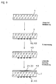
- the manufacturing process is divided into the three areas: processing of the carrier 7, processing of the semiconductor layer 11.3 and connection of the two parts.
- carrier 7 and semiconductor layer 11.3 can be processed either separately from one another or when they are already connected to one another.
- first the carrier 7 is processed and then either the already completed semiconductor layer 11.3 applied or the semiconductor layer is still processed after the connection with the carrier 7.
- first of all the semiconductor layer 11.3, possibly already finished can be applied to the carrier 7 and then the carrier 7 - and optionally the semiconductor layer 11.3 - finished.
- the order of processing of carrier 7, semiconductor layer 11.3 and their connection with each other can be chosen essentially freely, resulting in several alternative procedures. There is only the restriction that after connecting the semiconductor layer 11.3 with the side facing away from the scale 10 side of the carrier 7 on this side facing away from the scale 10 side of the carrier 7 no grid structures 8.1, 8.2 and 8.3 can be applied more.
- semiconductor material preferably silicon
- semiconductor material is applied in the desired thickness on the side of the carrier 7 facing away from the scale 10. This can be done in a CVD process or other methods known in the art. In this case, a crystalline, polycrystalline, amorphous, porous, microcrystalline or nanocrystalline semiconductor layer 11.3 is deposited.
- the semiconductor layer 11.3 may first be processed on a wafer and connected to the carrier 7 later.
- the semiconductor layer 11.3 can also be sputtered on and subsequently melted with a laser, so that after cooling of the semiconductor material, the required semiconductor layer 11.3 is formed.
- semiconductor material can be reduced by mechanical processing to a thickness of about 30 microns and then leached chemically.
- This thin semiconductor layer 11.3 is then connected to the carrier 7, for example by bonding methods.
- the photodiodes 2.1 and 2.2 are generated by appropriate doping of the areas in which the photodetectors are to be arranged. In this step, the generation of further modules such as amplifier and interpolator 12 can also be done.
- conductor tracks 3.1 and contacts 3.2, as well as metallic coatings 4.1 and 4.2 of the back sides of the photodiodes 2.1 and 2.2 are applied. This is done by applying a metallization layer of aluminum-titanium oxide, which is patterned according to known photochemical processes, on the semiconductor layer 11.3.
- the carrier 7 In the method for producing the carrier 7, it is possible to integrate a lens 1.1 in the carrier 7, which collimates the light of the light-emitting diode 1.
- a template for the lens is formed by electron beam lithography in a PMMA resist. The dose during the exposure with electrons is changed so that the shape of an optical lens 1.1 results after the development process. This is transmitted, for example by means of plasma etching, into the material of the carrier 7.
- phase gratings may be formed in the same manner as that just described for a lens on the carrier 7.
- Amplitude gratings are applied to the carrier 7 by known methods, for example as chrome gratings.
- connection of carrier 7 and semiconductor layer 11.3 can according to the FIGS. 8 . 9 and 10 done at any time. It is advantageous to carry out the connection when the carrier 7 and the semiconductor layer 11.3 have been finished, since then the carrier 7 and the semiconductor layer 11.3 can be processed separately, as in FIG FIG. 8 shown. Alternatively, it may be advantageous to deposit the semiconductor layer 11.3 directly on the carrier 7, which is in an arbitrary processing stage.
- semiconductor material can also be applied selectively only there on the support 7, where semiconductor components are also provided.
Landscapes
- Physics & Mathematics (AREA)
- General Physics & Mathematics (AREA)
- Optical Transform (AREA)
- Length Measuring Devices By Optical Means (AREA)
- Diffracting Gratings Or Hologram Optical Elements (AREA)
- Micromachines (AREA)
- Light Receiving Elements (AREA)
Priority Applications (1)
| Application Number | Priority Date | Filing Date | Title |
|---|---|---|---|
| EP07003460A EP1788361A3 (de) | 1999-04-21 | 2000-04-18 | Integrierter optoelektronischer Dünnschichtsensor für ein Linear-Verschiebungs-Messsystem |
Applications Claiming Priority (3)
| Application Number | Priority Date | Filing Date | Title |
|---|---|---|---|
| DE19917950 | 1999-04-21 | ||
| DE19917950A DE19917950A1 (de) | 1999-04-21 | 1999-04-21 | Integrierter optoelektronischer Dünnschichtsensor und Verfahren zu dessen Herstellung |
| PCT/EP2000/003509 WO2000063654A1 (de) | 1999-04-21 | 2000-04-18 | Integrierter optoelektronischer dünnschichtsensor und verfahren zu dessen herstellung |
Related Child Applications (2)
| Application Number | Title | Priority Date | Filing Date |
|---|---|---|---|
| EP07003460A Division EP1788361A3 (de) | 1999-04-21 | 2000-04-18 | Integrierter optoelektronischer Dünnschichtsensor für ein Linear-Verschiebungs-Messsystem |
| EP07003460.8 Division-Into | 2007-02-20 |
Publications (3)
| Publication Number | Publication Date |
|---|---|
| EP1175600A1 EP1175600A1 (de) | 2002-01-30 |
| EP1175600B1 EP1175600B1 (de) | 2007-02-28 |
| EP1175600B2 true EP1175600B2 (de) | 2010-10-27 |
Family
ID=7905268
Family Applications (2)
| Application Number | Title | Priority Date | Filing Date |
|---|---|---|---|
| EP00929380A Expired - Lifetime EP1175600B2 (de) | 1999-04-21 | 2000-04-18 | Integrierter optoelektronischer dünnschichtsensor |
| EP07003460A Ceased EP1788361A3 (de) | 1999-04-21 | 2000-04-18 | Integrierter optoelektronischer Dünnschichtsensor für ein Linear-Verschiebungs-Messsystem |
Family Applications After (1)
| Application Number | Title | Priority Date | Filing Date |
|---|---|---|---|
| EP07003460A Ceased EP1788361A3 (de) | 1999-04-21 | 2000-04-18 | Integrierter optoelektronischer Dünnschichtsensor für ein Linear-Verschiebungs-Messsystem |
Country Status (6)
| Country | Link |
|---|---|
| US (1) | US6621104B1 (enExample) |
| EP (2) | EP1175600B2 (enExample) |
| JP (1) | JP4688297B2 (enExample) |
| AT (1) | ATE355506T1 (enExample) |
| DE (2) | DE19917950A1 (enExample) |
| WO (1) | WO2000063654A1 (enExample) |
Families Citing this family (13)
| Publication number | Priority date | Publication date | Assignee | Title |
|---|---|---|---|---|
| JP4812189B2 (ja) * | 2001-06-15 | 2011-11-09 | オリンパス株式会社 | 光学式検出装置 |
| JP2003152299A (ja) * | 2001-07-10 | 2003-05-23 | Canon Inc | 配線接続構造及びその製造方法 |
| US7038288B2 (en) | 2002-09-25 | 2006-05-02 | Microsemi Corporation | Front side illuminated photodiode with backside bump |
| JP4021382B2 (ja) | 2003-07-28 | 2007-12-12 | オリンパス株式会社 | 光学式エンコーダ及びその製造方法並びに光学レンズモジュール |
| DE102004042670B4 (de) | 2003-09-02 | 2018-07-12 | CiS Forschungsinstitut für Mikrosensorik GmbH | Mikrooptisches Strahler- und Empfängersystem |
| GB0621487D0 (en) | 2006-10-28 | 2006-12-06 | Renishaw Plc | Opto-electronic read head |
| DE102010002902A1 (de) * | 2010-03-16 | 2011-09-22 | Dr. Johannes Heidenhain Gmbh | Abtasteinheit für eine optische Positionsmesseinrichtung |
| WO2012022003A1 (de) * | 2010-08-19 | 2012-02-23 | Elesta Relays Gmbh | Sensorkopfhalter |
| DE102015218702A1 (de) * | 2015-09-29 | 2017-03-30 | Dr. Johannes Heidenhain Gmbh | Optisches Schichtsystem |
| DE102018103869B3 (de) * | 2018-02-21 | 2019-05-09 | Physik Instrumente (Pi) Gmbh & Co. Kg | Maßelement für eine optische Messvorrichtung |
| CN111678888A (zh) * | 2020-06-09 | 2020-09-18 | 南方科技大学 | 一种液体折射率检测传感器、装置及方法 |
| US20240044675A1 (en) * | 2022-08-08 | 2024-02-08 | Hengstler Gmbh | Optoelectronic device comprising light processing device with a through-opening |
| EP4603801B1 (de) * | 2024-02-14 | 2025-12-31 | Sick Ag | Optischer encoder |
Citations (2)
| Publication number | Priority date | Publication date | Assignee | Title |
|---|---|---|---|---|
| DE3201185A1 (de) † | 1981-03-31 | 1982-10-14 | Jenoptik Jena Gmbh, Ddr 6900 Jena | Silizium-fotodetektor |
| DE19701941A1 (de) † | 1996-01-23 | 1997-07-24 | Mitutoyo Corp | Optischer Codierer |
Family Cites Families (25)
| Publication number | Priority date | Publication date | Assignee | Title |
|---|---|---|---|---|
| NL185178C (nl) | 1974-03-15 | 1990-02-01 | Nat Res Dev | Inrichting voor het foto-elektrisch meten van een relatieve verschuiving tussen twee elementen. |
| GB1504691A (en) | 1974-03-15 | 1978-03-22 | Nat Res Dev | Measurement apparatus |
| DE3625327C1 (de) | 1986-07-26 | 1988-02-18 | Heidenhain Gmbh Dr Johannes | Lichtelektrische Positionsmesseinrichtung |
| DE8717558U1 (de) | 1987-02-21 | 1989-02-23 | Dr. Johannes Heidenhain Gmbh, 8225 Traunreut | Lichtelektrische Positionsmeßeinrichtung |
| US5055894A (en) * | 1988-09-29 | 1991-10-08 | The Boeing Company | Monolithic interleaved LED/PIN photodetector array |
| DE3836703A1 (de) | 1988-10-28 | 1990-05-03 | Heidenhain Gmbh Dr Johannes | Winkelmesseinrichtung |
| JPH0656304B2 (ja) | 1989-09-05 | 1994-07-27 | 株式会社ミツトヨ | 光電型エンコーダ |
| ATE92622T1 (de) | 1989-12-23 | 1993-08-15 | Heidenhain Gmbh Dr Johannes | Einrichtung mit wenigstens einem wellenleiterkoppler. |
| DE4011718A1 (de) | 1990-04-11 | 1991-10-17 | Heidenhain Gmbh Dr Johannes | Integriert-optische sensoreinrichtung |
| US5204524A (en) * | 1991-03-22 | 1993-04-20 | Mitutoyo Corporation | Two-dimensional optical encoder with three gratings in each dimension |
| US5155355A (en) | 1991-04-25 | 1992-10-13 | Mitutoyo Corporation | Photoelectric encoder having a grating substrate with integral light emitting elements |
| DE59102268D1 (de) | 1991-05-24 | 1994-08-25 | Heidenhain Gmbh Dr Johannes | Vorrichtung zum Ein- und/oder Auskoppeln von Lichtstrahlen mit einem integriert-optischen Baustein. |
| EP0843159A3 (en) * | 1991-11-06 | 1999-06-02 | Renishaw Transducer Systems Limited | Opto-electronic scale-reading apparatus |
| SE470116B (sv) * | 1992-04-03 | 1993-11-08 | Asea Brown Boveri | Detektorkrets med en som detektor arbetande halvledardiod och en med dioden integrerad förstärkarkrets |
| DE4302313C2 (de) | 1993-01-28 | 1996-12-05 | Heidenhain Gmbh Dr Johannes | Mehrkoordinaten-Meßeinrichtung |
| JPH06268254A (ja) | 1993-03-15 | 1994-09-22 | Toshiba Corp | 半導体装置 |
| JP3082516B2 (ja) * | 1993-05-31 | 2000-08-28 | キヤノン株式会社 | 光学式変位センサおよび該光学式変位センサを用いた駆動システム |
| JP3244205B2 (ja) | 1993-06-17 | 2002-01-07 | 信越半導体株式会社 | 半導体装置 |
| JPH08178702A (ja) | 1994-12-27 | 1996-07-12 | Canon Inc | 光学式センサ |
| US5852322A (en) | 1995-05-19 | 1998-12-22 | Dr. Johannes Heidenhain Gmbh | Radiation-sensitive detector element and method for producing it |
| DE19524725C1 (de) | 1995-07-07 | 1996-07-11 | Zeiss Carl Jena Gmbh | Fotoelektrischer Kodierer zum Abtasten optischer Strukturen |
| DE19720300B4 (de) | 1996-06-03 | 2006-05-04 | CiS Institut für Mikrosensorik gGmbH | Elektronisches Hybrid-Bauelement und Verfahren zu seiner Herstellung |
| GB2315594B (en) * | 1996-07-22 | 2000-08-16 | Cambridge Display Tech Ltd | Sensing device |
| DE19859670A1 (de) | 1998-12-23 | 2000-06-29 | Heidenhain Gmbh Dr Johannes | Abtastkopf und Verfahren zu dessen Herstellung |
| DE19859669A1 (de) | 1998-12-23 | 2000-06-29 | Heidenhain Gmbh Dr Johannes | Integrierter optoelektronischer Sensor und Verfahren zu dessen Herstellung |
-
1999
- 1999-04-21 DE DE19917950A patent/DE19917950A1/de not_active Withdrawn
-
2000
- 2000-04-18 WO PCT/EP2000/003509 patent/WO2000063654A1/de not_active Ceased
- 2000-04-18 DE DE50014119T patent/DE50014119D1/de not_active Expired - Lifetime
- 2000-04-18 US US09/959,357 patent/US6621104B1/en not_active Expired - Fee Related
- 2000-04-18 EP EP00929380A patent/EP1175600B2/de not_active Expired - Lifetime
- 2000-04-18 AT AT00929380T patent/ATE355506T1/de not_active IP Right Cessation
- 2000-04-18 JP JP2000612707A patent/JP4688297B2/ja not_active Expired - Fee Related
- 2000-04-18 EP EP07003460A patent/EP1788361A3/de not_active Ceased
Patent Citations (2)
| Publication number | Priority date | Publication date | Assignee | Title |
|---|---|---|---|---|
| DE3201185A1 (de) † | 1981-03-31 | 1982-10-14 | Jenoptik Jena Gmbh, Ddr 6900 Jena | Silizium-fotodetektor |
| DE19701941A1 (de) † | 1996-01-23 | 1997-07-24 | Mitutoyo Corp | Optischer Codierer |
Also Published As
| Publication number | Publication date |
|---|---|
| EP1788361A2 (de) | 2007-05-23 |
| US6621104B1 (en) | 2003-09-16 |
| EP1175600B1 (de) | 2007-02-28 |
| DE50014119D1 (de) | 2007-04-12 |
| EP1788361A3 (de) | 2007-05-30 |
| ATE355506T1 (de) | 2006-03-15 |
| JP4688297B2 (ja) | 2011-05-25 |
| EP1175600A1 (de) | 2002-01-30 |
| DE19917950A1 (de) | 2000-10-26 |
| WO2000063654A1 (de) | 2000-10-26 |
| JP2002542616A (ja) | 2002-12-10 |
Similar Documents
| Publication | Publication Date | Title |
|---|---|---|
| EP1014034B1 (de) | Integrierter optoelektronischer Sensor und Verfahren zu dessen Herstellung | |
| EP1175600B2 (de) | Integrierter optoelektronischer dünnschichtsensor | |
| EP1014043B1 (de) | Abtastkopf | |
| DE69320716T2 (de) | Gerät zur Detektion von Verschiebungsinformation | |
| DE10133266A1 (de) | Lichtfleckpositionssensor und Auslenkungsmessgerät | |
| DE19618593A1 (de) | Strahlungsempfindliches Detektorelement und Verfahren zur Herstellung desselben | |
| DE102007042984A1 (de) | Vorrichtung zur optischen Navigation | |
| DE112014002312T5 (de) | Integrierte Bildgebungsvorrichtung für Infrarotstrahlung und Herstellungsverfahren | |
| EP2520906A1 (de) | Optische Positionsmesseinrichtung | |
| DE3220560A1 (de) | Fotoelektrischer kodierer | |
| EP1436647B1 (de) | Verfahren zur herstellung eines massstabes, sowie derart hergestellter massstab und eine positionsmesseinrichtung | |
| DE10159855A1 (de) | Optischer Codierer | |
| DE3209043C2 (de) | Fotoelektrische Bewegungs-Meßeinrichtung | |
| DE69101393T2 (de) | Kodierer. | |
| DE10022676A1 (de) | Optische Verschiebungsdetektoreinrichtung | |
| DE10037981A1 (de) | Verschiebungsmessvorrichtung | |
| DE10328873B4 (de) | Codierer vom Projektionstyp | |
| EP1695391A1 (de) | Abtastkopf für optische positionsmesssysteme | |
| DE4091517C2 (de) | Photoelektrische Codiereinrichtung | |
| DE102020200098A1 (de) | LIDAR-Sensor und Verfahren zur optischen Erfassung eines Sichtfeldes | |
| DE10131608B4 (de) | Photosensor für ein Durchlichtverfahren zur Detektion der Bewegungsrichtung von Intensitätsmaxima und Intensitätsminima einer optischen stehenden Welle | |
| DE10013813A1 (de) | Optischer Kodierer | |
| DE19518303C2 (de) | Optische Linsen-/Detektoranordnung | |
| DE102004022569A1 (de) | Projektionscodierer | |
| DE3828050C2 (enExample) |
Legal Events
| Date | Code | Title | Description |
|---|---|---|---|
| PUAI | Public reference made under article 153(3) epc to a published international application that has entered the european phase |
Free format text: ORIGINAL CODE: 0009012 |
|
| 17P | Request for examination filed |
Effective date: 20011121 |
|
| AK | Designated contracting states |
Kind code of ref document: A1 Designated state(s): AT BE CH CY DE DK ES FI FR GB GR IE IT LI LU MC NL PT SE |
|
| 17Q | First examination report despatched |
Effective date: 20050811 |
|
| GRAP | Despatch of communication of intention to grant a patent |
Free format text: ORIGINAL CODE: EPIDOSNIGR1 |
|
| RTI1 | Title (correction) |
Free format text: INTEGRATED OPTOELECTRONIC THIN-FILM SENSOR |
|
| GRAS | Grant fee paid |
Free format text: ORIGINAL CODE: EPIDOSNIGR3 |
|
| GRAA | (expected) grant |
Free format text: ORIGINAL CODE: 0009210 |
|
| AK | Designated contracting states |
Kind code of ref document: B1 Designated state(s): AT BE CH CY DE DK ES FI FR GB GR IE IT LI LU MC NL PT SE |
|
| PG25 | Lapsed in a contracting state [announced via postgrant information from national office to epo] |
Ref country code: IE Free format text: LAPSE BECAUSE OF FAILURE TO SUBMIT A TRANSLATION OF THE DESCRIPTION OR TO PAY THE FEE WITHIN THE PRESCRIBED TIME-LIMIT Effective date: 20070228 Ref country code: NL Free format text: LAPSE BECAUSE OF FAILURE TO SUBMIT A TRANSLATION OF THE DESCRIPTION OR TO PAY THE FEE WITHIN THE PRESCRIBED TIME-LIMIT Effective date: 20070228 Ref country code: DK Free format text: LAPSE BECAUSE OF FAILURE TO SUBMIT A TRANSLATION OF THE DESCRIPTION OR TO PAY THE FEE WITHIN THE PRESCRIBED TIME-LIMIT Effective date: 20070228 Ref country code: FI Free format text: LAPSE BECAUSE OF FAILURE TO SUBMIT A TRANSLATION OF THE DESCRIPTION OR TO PAY THE FEE WITHIN THE PRESCRIBED TIME-LIMIT Effective date: 20070228 |
|
| REG | Reference to a national code |
Ref country code: GB Ref legal event code: FG4D Free format text: NOT ENGLISH |
|
| GBT | Gb: translation of ep patent filed (gb section 77(6)(a)/1977) |
Effective date: 20070228 |
|
| REG | Reference to a national code |
Ref country code: CH Ref legal event code: NV Representative=s name: TROESCH SCHEIDEGGER WERNER AG Ref country code: CH Ref legal event code: EP |
|
| REF | Corresponds to: |
Ref document number: 50014119 Country of ref document: DE Date of ref document: 20070412 Kind code of ref document: P |
|
| REG | Reference to a national code |
Ref country code: IE Ref legal event code: FG4D Free format text: LANGUAGE OF EP DOCUMENT: GERMAN |
|
| PG25 | Lapsed in a contracting state [announced via postgrant information from national office to epo] |
Ref country code: SE Free format text: LAPSE BECAUSE OF FAILURE TO SUBMIT A TRANSLATION OF THE DESCRIPTION OR TO PAY THE FEE WITHIN THE PRESCRIBED TIME-LIMIT Effective date: 20070531 |
|
| PG25 | Lapsed in a contracting state [announced via postgrant information from national office to epo] |
Ref country code: ES Free format text: LAPSE BECAUSE OF FAILURE TO SUBMIT A TRANSLATION OF THE DESCRIPTION OR TO PAY THE FEE WITHIN THE PRESCRIBED TIME-LIMIT Effective date: 20070608 |
|
| ET | Fr: translation filed | ||
| PG25 | Lapsed in a contracting state [announced via postgrant information from national office to epo] |
Ref country code: PT Free format text: LAPSE BECAUSE OF FAILURE TO SUBMIT A TRANSLATION OF THE DESCRIPTION OR TO PAY THE FEE WITHIN THE PRESCRIBED TIME-LIMIT Effective date: 20070730 |
|
| NLV1 | Nl: lapsed or annulled due to failure to fulfill the requirements of art. 29p and 29m of the patents act | ||
| REG | Reference to a national code |
Ref country code: IE Ref legal event code: FD4D |
|
| PLBI | Opposition filed |
Free format text: ORIGINAL CODE: 0009260 |
|
| BERE | Be: lapsed |
Owner name: DR. JOHANNES HEIDENHAIN G.M.B.H. Effective date: 20070430 |
|
| 26 | Opposition filed |
Opponent name: SICK STEGMANN GMBH Effective date: 20071128 |
|
| PLAX | Notice of opposition and request to file observation + time limit sent |
Free format text: ORIGINAL CODE: EPIDOSNOBS2 |
|
| PG25 | Lapsed in a contracting state [announced via postgrant information from national office to epo] |
Ref country code: BE Free format text: LAPSE BECAUSE OF NON-PAYMENT OF DUE FEES Effective date: 20070430 |
|
| PG25 | Lapsed in a contracting state [announced via postgrant information from national office to epo] |
Ref country code: IT Free format text: LAPSE BECAUSE OF FAILURE TO SUBMIT A TRANSLATION OF THE DESCRIPTION OR TO PAY THE FEE WITHIN THE PRESCRIBED TIME-LIMIT Effective date: 20070228 Ref country code: GR Free format text: LAPSE BECAUSE OF FAILURE TO SUBMIT A TRANSLATION OF THE DESCRIPTION OR TO PAY THE FEE WITHIN THE PRESCRIBED TIME-LIMIT Effective date: 20070529 |
|
| PLAF | Information modified related to communication of a notice of opposition and request to file observations + time limit |
Free format text: ORIGINAL CODE: EPIDOSCOBS2 |
|
| PG25 | Lapsed in a contracting state [announced via postgrant information from national office to epo] |
Ref country code: AT Free format text: LAPSE BECAUSE OF NON-PAYMENT OF DUE FEES Effective date: 20070418 |
|
| PLBB | Reply of patent proprietor to notice(s) of opposition received |
Free format text: ORIGINAL CODE: EPIDOSNOBS3 |
|
| PG25 | Lapsed in a contracting state [announced via postgrant information from national office to epo] |
Ref country code: MC Free format text: LAPSE BECAUSE OF NON-PAYMENT OF DUE FEES Effective date: 20070430 |
|
| PG25 | Lapsed in a contracting state [announced via postgrant information from national office to epo] |
Ref country code: CY Free format text: LAPSE BECAUSE OF FAILURE TO SUBMIT A TRANSLATION OF THE DESCRIPTION OR TO PAY THE FEE WITHIN THE PRESCRIBED TIME-LIMIT Effective date: 20070228 |
|
| PG25 | Lapsed in a contracting state [announced via postgrant information from national office to epo] |
Ref country code: LU Free format text: LAPSE BECAUSE OF NON-PAYMENT OF DUE FEES Effective date: 20070418 |
|
| PUAH | Patent maintained in amended form |
Free format text: ORIGINAL CODE: 0009272 |
|
| STAA | Information on the status of an ep patent application or granted ep patent |
Free format text: STATUS: PATENT MAINTAINED AS AMENDED |
|
| 27A | Patent maintained in amended form |
Effective date: 20101027 |
|
| AK | Designated contracting states |
Kind code of ref document: B2 Designated state(s): AT BE CH CY DE DK ES FI FR GB GR IE IT LI LU MC NL PT SE |
|
| REG | Reference to a national code |
Ref country code: CH Ref legal event code: AEN Free format text: AUFRECHTERHALTUNG DES PATENTES IN GEAENDERTER FORM |
|
| REG | Reference to a national code |
Ref country code: FR Ref legal event code: PLFP Year of fee payment: 16 |
|
| PGFP | Annual fee paid to national office [announced via postgrant information from national office to epo] |
Ref country code: GB Payment date: 20150420 Year of fee payment: 16 Ref country code: CH Payment date: 20150420 Year of fee payment: 16 |
|
| PGFP | Annual fee paid to national office [announced via postgrant information from national office to epo] |
Ref country code: FR Payment date: 20150421 Year of fee payment: 16 |
|
| REG | Reference to a national code |
Ref country code: CH Ref legal event code: PL |
|
| GBPC | Gb: european patent ceased through non-payment of renewal fee |
Effective date: 20160418 |
|
| REG | Reference to a national code |
Ref country code: FR Ref legal event code: ST Effective date: 20161230 |
|
| PG25 | Lapsed in a contracting state [announced via postgrant information from national office to epo] |
Ref country code: CH Free format text: LAPSE BECAUSE OF NON-PAYMENT OF DUE FEES Effective date: 20160430 Ref country code: GB Free format text: LAPSE BECAUSE OF NON-PAYMENT OF DUE FEES Effective date: 20160418 Ref country code: LI Free format text: LAPSE BECAUSE OF NON-PAYMENT OF DUE FEES Effective date: 20160430 Ref country code: FR Free format text: LAPSE BECAUSE OF NON-PAYMENT OF DUE FEES Effective date: 20160502 |
|
| PGFP | Annual fee paid to national office [announced via postgrant information from national office to epo] |
Ref country code: DE Payment date: 20170419 Year of fee payment: 18 |
|
| REG | Reference to a national code |
Ref country code: DE Ref legal event code: R119 Ref document number: 50014119 Country of ref document: DE |
|
| PG25 | Lapsed in a contracting state [announced via postgrant information from national office to epo] |
Ref country code: DE Free format text: LAPSE BECAUSE OF NON-PAYMENT OF DUE FEES Effective date: 20181101 |