EP1174921A2 - Semiconductor device - Google Patents
Semiconductor device Download PDFInfo
- Publication number
- EP1174921A2 EP1174921A2 EP01305966A EP01305966A EP1174921A2 EP 1174921 A2 EP1174921 A2 EP 1174921A2 EP 01305966 A EP01305966 A EP 01305966A EP 01305966 A EP01305966 A EP 01305966A EP 1174921 A2 EP1174921 A2 EP 1174921A2
- Authority
- EP
- European Patent Office
- Prior art keywords
- lead frame
- base substrate
- semiconductor device
- insulating layer
- bent
- Prior art date
- Legal status (The legal status is an assumption and is not a legal conclusion. Google has not performed a legal analysis and makes no representation as to the accuracy of the status listed.)
- Granted
Links
Images




Classifications
-
- H—ELECTRICITY
- H10—SEMICONDUCTOR DEVICES; ELECTRIC SOLID-STATE DEVICES NOT OTHERWISE PROVIDED FOR
- H10W—GENERIC PACKAGES, INTERCONNECTIONS, CONNECTORS OR OTHER CONSTRUCTIONAL DETAILS OF DEVICES COVERED BY CLASS H10
- H10W72/00—Interconnections or connectors in packages
- H10W72/01—Manufacture or treatment
- H10W72/013—Manufacture or treatment of die-attach connectors
-
- H—ELECTRICITY
- H10—SEMICONDUCTOR DEVICES; ELECTRIC SOLID-STATE DEVICES NOT OTHERWISE PROVIDED FOR
- H10W—GENERIC PACKAGES, INTERCONNECTIONS, CONNECTORS OR OTHER CONSTRUCTIONAL DETAILS OF DEVICES COVERED BY CLASS H10
- H10W70/00—Package substrates; Interposers; Redistribution layers [RDL]
- H10W70/40—Leadframes
-
- H—ELECTRICITY
- H10—SEMICONDUCTOR DEVICES; ELECTRIC SOLID-STATE DEVICES NOT OTHERWISE PROVIDED FOR
- H10W—GENERIC PACKAGES, INTERCONNECTIONS, CONNECTORS OR OTHER CONSTRUCTIONAL DETAILS OF DEVICES COVERED BY CLASS H10
- H10W70/00—Package substrates; Interposers; Redistribution layers [RDL]
- H10W70/40—Leadframes
- H10W70/479—Leadframes on or in insulating or insulated package substrates, interposers, or redistribution layers
-
- H—ELECTRICITY
- H10—SEMICONDUCTOR DEVICES; ELECTRIC SOLID-STATE DEVICES NOT OTHERWISE PROVIDED FOR
- H10W—GENERIC PACKAGES, INTERCONNECTIONS, CONNECTORS OR OTHER CONSTRUCTIONAL DETAILS OF DEVICES COVERED BY CLASS H10
- H10W90/00—Package configurations
-
- H—ELECTRICITY
- H10—SEMICONDUCTOR DEVICES; ELECTRIC SOLID-STATE DEVICES NOT OTHERWISE PROVIDED FOR
- H10W—GENERIC PACKAGES, INTERCONNECTIONS, CONNECTORS OR OTHER CONSTRUCTIONAL DETAILS OF DEVICES COVERED BY CLASS H10
- H10W72/00—Interconnections or connectors in packages
- H10W72/071—Connecting or disconnecting
- H10W72/073—Connecting or disconnecting of die-attach connectors
-
- H—ELECTRICITY
- H10—SEMICONDUCTOR DEVICES; ELECTRIC SOLID-STATE DEVICES NOT OTHERWISE PROVIDED FOR
- H10W—GENERIC PACKAGES, INTERCONNECTIONS, CONNECTORS OR OTHER CONSTRUCTIONAL DETAILS OF DEVICES COVERED BY CLASS H10
- H10W72/00—Interconnections or connectors in packages
- H10W72/071—Connecting or disconnecting
- H10W72/073—Connecting or disconnecting of die-attach connectors
- H10W72/07331—Connecting techniques
- H10W72/07336—Soldering or alloying
-
- H—ELECTRICITY
- H10—SEMICONDUCTOR DEVICES; ELECTRIC SOLID-STATE DEVICES NOT OTHERWISE PROVIDED FOR
- H10W—GENERIC PACKAGES, INTERCONNECTIONS, CONNECTORS OR OTHER CONSTRUCTIONAL DETAILS OF DEVICES COVERED BY CLASS H10
- H10W72/00—Interconnections or connectors in packages
- H10W72/071—Connecting or disconnecting
- H10W72/075—Connecting or disconnecting of bond wires
-
- H—ELECTRICITY
- H10—SEMICONDUCTOR DEVICES; ELECTRIC SOLID-STATE DEVICES NOT OTHERWISE PROVIDED FOR
- H10W—GENERIC PACKAGES, INTERCONNECTIONS, CONNECTORS OR OTHER CONSTRUCTIONAL DETAILS OF DEVICES COVERED BY CLASS H10
- H10W72/00—Interconnections or connectors in packages
- H10W72/071—Connecting or disconnecting
- H10W72/075—Connecting or disconnecting of bond wires
- H10W72/07551—Connecting or disconnecting of bond wires characterised by changes in properties of the bond wires during the connecting
- H10W72/07554—Connecting or disconnecting of bond wires characterised by changes in properties of the bond wires during the connecting changes in dispositions
-
- H—ELECTRICITY
- H10—SEMICONDUCTOR DEVICES; ELECTRIC SOLID-STATE DEVICES NOT OTHERWISE PROVIDED FOR
- H10W—GENERIC PACKAGES, INTERCONNECTIONS, CONNECTORS OR OTHER CONSTRUCTIONAL DETAILS OF DEVICES COVERED BY CLASS H10
- H10W72/00—Interconnections or connectors in packages
- H10W72/30—Die-attach connectors
- H10W72/351—Materials of die-attach connectors
- H10W72/353—Materials of die-attach connectors not comprising solid metals or solid metalloids, e.g. ceramics
- H10W72/354—Materials of die-attach connectors not comprising solid metals or solid metalloids, e.g. ceramics comprising polymers
-
- H—ELECTRICITY
- H10—SEMICONDUCTOR DEVICES; ELECTRIC SOLID-STATE DEVICES NOT OTHERWISE PROVIDED FOR
- H10W—GENERIC PACKAGES, INTERCONNECTIONS, CONNECTORS OR OTHER CONSTRUCTIONAL DETAILS OF DEVICES COVERED BY CLASS H10
- H10W72/00—Interconnections or connectors in packages
- H10W72/50—Bond wires
- H10W72/541—Dispositions of bond wires
- H10W72/547—Dispositions of multiple bond wires
-
- H—ELECTRICITY
- H10—SEMICONDUCTOR DEVICES; ELECTRIC SOLID-STATE DEVICES NOT OTHERWISE PROVIDED FOR
- H10W—GENERIC PACKAGES, INTERCONNECTIONS, CONNECTORS OR OTHER CONSTRUCTIONAL DETAILS OF DEVICES COVERED BY CLASS H10
- H10W72/00—Interconnections or connectors in packages
- H10W72/50—Bond wires
- H10W72/551—Materials of bond wires
- H10W72/552—Materials of bond wires comprising metals or metalloids, e.g. silver
- H10W72/5524—Materials of bond wires comprising metals or metalloids, e.g. silver comprising aluminium [Al]
-
- H—ELECTRICITY
- H10—SEMICONDUCTOR DEVICES; ELECTRIC SOLID-STATE DEVICES NOT OTHERWISE PROVIDED FOR
- H10W—GENERIC PACKAGES, INTERCONNECTIONS, CONNECTORS OR OTHER CONSTRUCTIONAL DETAILS OF DEVICES COVERED BY CLASS H10
- H10W72/00—Interconnections or connectors in packages
- H10W72/851—Dispositions of multiple connectors or interconnections
- H10W72/874—On different surfaces
- H10W72/884—Die-attach connectors and bond wires
-
- H—ELECTRICITY
- H10—SEMICONDUCTOR DEVICES; ELECTRIC SOLID-STATE DEVICES NOT OTHERWISE PROVIDED FOR
- H10W—GENERIC PACKAGES, INTERCONNECTIONS, CONNECTORS OR OTHER CONSTRUCTIONAL DETAILS OF DEVICES COVERED BY CLASS H10
- H10W74/00—Encapsulations, e.g. protective coatings
-
- H—ELECTRICITY
- H10—SEMICONDUCTOR DEVICES; ELECTRIC SOLID-STATE DEVICES NOT OTHERWISE PROVIDED FOR
- H10W—GENERIC PACKAGES, INTERCONNECTIONS, CONNECTORS OR OTHER CONSTRUCTIONAL DETAILS OF DEVICES COVERED BY CLASS H10
- H10W90/00—Package configurations
- H10W90/701—Package configurations characterised by the relative positions of pads or connectors relative to package parts
- H10W90/731—Package configurations characterised by the relative positions of pads or connectors relative to package parts of die-attach connectors
- H10W90/736—Package configurations characterised by the relative positions of pads or connectors relative to package parts of die-attach connectors between a chip and a stacked lead frame, conducting package substrate or heat sink
-
- H—ELECTRICITY
- H10—SEMICONDUCTOR DEVICES; ELECTRIC SOLID-STATE DEVICES NOT OTHERWISE PROVIDED FOR
- H10W—GENERIC PACKAGES, INTERCONNECTIONS, CONNECTORS OR OTHER CONSTRUCTIONAL DETAILS OF DEVICES COVERED BY CLASS H10
- H10W90/00—Package configurations
- H10W90/701—Package configurations characterised by the relative positions of pads or connectors relative to package parts
- H10W90/751—Package configurations characterised by the relative positions of pads or connectors relative to package parts of bond wires
- H10W90/753—Package configurations characterised by the relative positions of pads or connectors relative to package parts of bond wires between laterally-adjacent chips
-
- H—ELECTRICITY
- H10—SEMICONDUCTOR DEVICES; ELECTRIC SOLID-STATE DEVICES NOT OTHERWISE PROVIDED FOR
- H10W—GENERIC PACKAGES, INTERCONNECTIONS, CONNECTORS OR OTHER CONSTRUCTIONAL DETAILS OF DEVICES COVERED BY CLASS H10
- H10W90/00—Package configurations
- H10W90/701—Package configurations characterised by the relative positions of pads or connectors relative to package parts
- H10W90/751—Package configurations characterised by the relative positions of pads or connectors relative to package parts of bond wires
- H10W90/754—Package configurations characterised by the relative positions of pads or connectors relative to package parts of bond wires between a chip and a stacked insulating package substrate, interposer or RDL
-
- H—ELECTRICITY
- H10—SEMICONDUCTOR DEVICES; ELECTRIC SOLID-STATE DEVICES NOT OTHERWISE PROVIDED FOR
- H10W—GENERIC PACKAGES, INTERCONNECTIONS, CONNECTORS OR OTHER CONSTRUCTIONAL DETAILS OF DEVICES COVERED BY CLASS H10
- H10W90/00—Package configurations
- H10W90/701—Package configurations characterised by the relative positions of pads or connectors relative to package parts
- H10W90/751—Package configurations characterised by the relative positions of pads or connectors relative to package parts of bond wires
- H10W90/756—Package configurations characterised by the relative positions of pads or connectors relative to package parts of bond wires between a chip and a stacked lead frame, conducting package substrate or heat sink
Definitions
- the present invention relates to a semiconductor device in which one or more of power semiconductor elements is/are mounted on a lead frame and then this assembly is insertionally molded with a resin and, particularly, to a semiconductor device in which a portion of the lead frame serving as an outward guided terminal stands up generally perpendicularly from the lead frame.
- the so-called a semiconductor device composed of a lead frame in which device the lead frame is used as a circuit conductor and one or more of power semiconductor elements is/are mounted on one surface of the lead frame and then a base substrate made from a metal having excellent thermal conductivity is joined to the other surface of the lead frame via a resin insulating layer, which is designed for realizing the compatibility between high dielectric withstanding voltage and low thermal resistance characteristics.
- FIG. 8 shows an example of this semiconductor device composed of the lead frame, which is disclosed in JP-A-11-42663.
- a lead frame 13 is used, which frame is formed substantially integrally from a conductor plate of copper, etc. having a uniform thickness.
- This lead frame 13 is adhered to one surface (a top side surface) of a metal base substrate 15 via an insulating layer 18, whereby the lead frame can play a role as a pattern of the conductor on a usual circuit board.
- a predetermined end portion of the lead frame 13 is bent so that it stands up generally perpendicularly from the bonding surface of the base substrate 15 and thus an outward guided terminal portion 17 is formed.
- the outward guided terminal portion 17 and one or more of power semiconductor elements 11 are electrically connected with each other to the lead frame 13 by mounting the power semiconductor elements 11 on the lead frame 13, and necessary portions are connected with each other by an aluminum bonding wire 16, whereby necessary circuits such as the main circuit, etc. of a power converter are formed.
- the reason why the lead frame 13 is bent perpendicularly to the surface of the base substrate 15 is to keep an insulation distance from the base substrate 15.
- the bending position of the lead frame 13 comes inward from an end surface of the base substrate 15 toward the center thereof (right direction).
- the lead frame 13 is adhered to the one surface (a top surface) of the base substrate 15 via the thin insulating layer 18 and, therefore, the heat generated by the power semiconductor elements 11 are conducted to the base substrate 15 via the insulating layer 18, thereby ensuring the dissipation of heat. Therefore, this base substrate 15 is fabricated from a metal plate composing a metal such as aluminum and copper, which are excellent in thermal conductivity.
- the insulating layer 18 serves to adhere the lead frame 13 to the base substrate 15 and serves the function of physically spacing both apart and electrically insulating therebetween with each other.
- the insulating layer 18 is made from a thermosetting resin such as an epoxy resin having a glassy-transition temperature of not less than 100°C and this material is used in the form of a resin sheet.
- a molded outer package (not shown) is adhered to the base substrate 15 by an adhesive or the like, in which package a resin such as an epoxy resin is filled.
- package a resin such as an epoxy resin
- the terminal portion 17 stands up generally perpendicularly from the bonding surface of the lead frame to be fixedly adhered to the surface of the base substrate, it is necessary to form the lead frame in such a manner that the terminal portion is bent beforehand and then to adhere this bent lead frame to the base substrate.
- a lead frame 13 is prepared, which frame is bent beforehand so as to form an outward guided terminal portion 17.
- This lead frame 13 is placed on the surface of a base substrate 15 with an insulation resin sheet 18' for insulative adhesion interposed therebetween, and is then heated under pressure to thereby obtain the state shown in FIG. 9(b).
- the resin sheet 18' sets hard and thereafter forms an insulating layer 18.
- the lead frame 13 is fixedly adhered to the surface of the base substrate 15.
- solder printing treatment necessary for the formation of a solder layer 26 is exerted on the surface of the lead frame 13 for mounting one or more of the semiconductor elements 11 thereon.
- the semiconductor elements 11 are superimposed on the solder layer 26 and the semiconductor elements 11 are joined to the lead frame 13 by heating under pressure. After that, a predetermined wiring is performed by means of a bonding wire 16.
- the outward guided terminal portion 17 stands up from the lead frame 13 and, therefore, first of all, in the step of FIG. 9(a), it is necessary to prevent the interference (i.e., the collision) of the outward guided terminal portion 17 with a compression press and the like. This leads to an increase in equipment size and hence an increase in the amount of investment.
- a mask and a squeegee for solder layer printing interfere with the outward guided terminal portion 17. Therefore, it is difficult to perform solder printing treatment for forming the solder layer 26 on the lead frame 13 and techniques such as screen printing cannot be applied thereto.
- the outward guided terminal portion 17 stands a great physical difficulties to the operating range of mounting equipment necessary for mounting parts on the lead frame 13 and it is difficult to solve this problem with a usual mounting equipment.
- the object of the present invention is to provide a semiconductor device composed of a lead frame in which the possibility of a complicated manufacturing process is prevented and a reduction in manufacturing cost can be satisfactorily achieved.
- the invention provides a semiconductor device in which a lead frame fixedly adhered via an insulating layer to one surface of a base substrate serves as a circuit conductor and on which frame one or more of semiconductors are mounted so as to bend an end portion of said lead frame in a stand-up direction from the bonding surface of the lead frame to be fixedly adhered to the surface of said base substrate as an outward guided terminal portion, wherein, in a portion of the lead frame, there is formed a recessed portion whose thickness is reduced from the bonding surface of the lead frame to be fixedly adhered to the surface of the base substrate and the lead frame is bent at this recessed portion having a reduced thickness.
- the stand-up position of the lead frame from the surface of the base substrate may be spaced apart by a predetermined specific distance from an end surface of the base substrate.
- a curved portion following a straight portion may also be formed in a stand-up portion of the lead frame from the surface of the base substrate.
- FIG. 1 shows a first embodiment of a semiconductor device according to the present invention.
- one or more of power semiconductor elements 11, a lead frame 13, a base substrate 15, a bonding wire 16, an outward guided terminal portion 17 and a solder layer 26 are the same as in the prior art device as described in FIG. 8.
- the terminal that is guided to outside the package of the semiconductor device as the outward guided terminal portion 17 is extended on the base substrate 15 inside the package to form the lead frame 13.
- This lead frame 13 is fixedly adhered to the base substrate 15 with the insulating layer 18 interposed therebetween, and the power semiconductor elements 11 are directly joined to the lead frame 13 via the solder layer 26.
- the lead frame 13 and the power semiconductor elements 11 are each electrically connected by the bonding wire 16 represented by an aluminum wire to form a predetermined circuit.
- the direction to which the lead frame 13 is to be guided as the outward guided terminal portion 17 must be perpendicular to the surface of the base substrate 15 in order to ensure a necessary insulation distance and, for this reason, the position where the lead frame 13 is perpendicularly (upward direction) bent must be spaced inside by a distance of not less than d4 from an end surface of the base substrate 15 toward the center direction (right direction) of the base substrate 15.
- the distance d4 from an end surface of the base substrate 15 is determined by a voltage applied between the lead frame 13 and the base substrate 15 and is primarily determined by dielectric withstand voltage characteristic required for the semiconductor device.
- the embodiment shown in FIG. 1 differs from that of the prior art shown in FIG. 8 in that the lead frame 13 includes portions each having different thicknesses of d1 and d2, respectively.
- the thickness of the lead frame 13 is adapted to be d1 (fixedly adhered portion) in a portion where the lead frame 13 is fixedly adhered to the base substrate 15 with the insulating layer 18 interposed therebetween while the thickness of the lead frame is adapted to be d2 in another portion 130 of the lead frame 13 where the lead frame 13 is bent in order to form the outward guided terminal portion 17, wherein the relationship therebetween is d1 > d2 and this portion 130 having a reduced thickness is formed on the lead frame 13 in a manner such that the thickness is reduced from the bonding surface of the lead frame 13 which is fixedly adhered to the base substrate 15 via the insulating layer 18.
- the lead frame 13 of the embodiment shown in FIG. 1 differs from the prior art in that it is formed with the portion 130 having a reduced thickness, and in that the lead frame 13 is bent in this portion 130 to form the outward guided portion 17 in a perpendicular standing upright position.
- the lead frame 13 on which this portion 130 is formed beforehand is superimposed on the insulating layer 18 in a flat state and is fixedly adhered to the base substrate 15. After the mounting of parts, the lead frame 13 is perpendicularly bent at a predetermined position of the base substrate 15 to thereby form the outward guided terminal portion 17.
- a longitudinally extending portion of the lead frame 13 is formed with the portion 130 having a reduced thickness.
- the length d5 it is adapted to be longer than the distance d4 necessary for insulation, that is, it is ensured that the relationship therebetween is held true to be d5 > d4 and in addition to the above the lead frame 13 is adapted to be bent in this portion 130 when forming the outward guided portion 17.
- the portion 130 provided in the lead frame 13 is formed, as mentioned above, on the lead frame 13 as a recessed portion from the surface on which the lead frame 13 is fixedly adhered to the base substrate 15. For this reason, even when the lead frame 13 is fixedly adhered to the base substrate 15 via the insulating layer 18 as it is, the lead frame 13 is spaced apart at a predetermined distance from the insulating layer 18 in this portion 130 and works so that it keeps a state in which the lead frame 13 is not fixedly adhered to the base substrate 15 in this portion 130.
- this lead frame 13 is perpendicularly bent to thereby form the outward guided terminal portion 17, it can be ensured that there is no possibility of damage to the insulating layer 18 at all.
- the lead frame 13 having a reduced thickness portion 130 is prepared and superimposed on the base substrate 15 in a flat state with the resin sheet 18' interposed therebetween, and the lead frame 13 is fixedly adhered to the base substrate 15 by heating under pressure after predetermined positioning, whereby as shown in FIG. 2(b), the lead frame 13 in a flat state is adapted to be fixedly adhered to the base substrate 15 via the insulating layer 18.
- this level difference is not limited to the above numerical values and may be arbitrarily determined according to the thickness of the lead frame 13 and specifications for the insulating layer 18.
- the condition that it is longer than the above distance d4 required for insulation, i.e., the relationship therebetween of d5 > d4 may be preferably kept.
- the portion 130 is not restricted to be formed in only the peripheral end portion of the base substrate 15 and but may be extended to the leading end of the outward guided terminal portion 17. Therefore, the dimensional conditions necessary for the lead frame 13 are d1 > d2 and d4 ⁇ d5.
- a predetermined portion of the lead frame 13, i.e., the portion on which one or more of power semiconductor elements are mounted is subjected to solder printing treatment necessary for the formation of the solder layer 26 and after that, as shown in FIG. 2(c), the semiconductor elements 11 are positioned. Subsequently, as shown in FIG. 2(d), the semiconductor elements 11 are joined to the lead frame 13 via the solder layer 26 and wiring is then performed by means of the bonding wire 16.
- an end portion of the lead frame 13 (left side end) is held by means of a predetermined jig from the upper side in the figure so that the lead frame 13 is not stripped off from the insulating layer 15 and then, as indicated by the arrow A in FIG. 2(c), the outward guided terminal portion 17 is formed by standing the lead frame 13 up generally perpendicularly to the surface of the base substrate 15, whereby a semiconductor device in a state shown in FIG. 1 can be obtained.
- the lead frame 13 when the lead frame 13 is fixedly adhered to the base substrate 15 via the insulating layer 18, the lead frame 13 is superimposed in a flat state on the insulating layer 18 and there are no any obstacles on the surface of the lead frame 13.
- the interference by the stand-up portion of the lead frame 13 does not occur during the mounting of parts or wire bonding. Therefore, according to this embodiment, the limitation for various kinds of equipment to be used in the assembling steps shown in FIGS. 2(a) to 2(d) can be minimized and hence a cost rise can be efficiently reduced.
- the lead frame 13 may have a flat shape as it is, this lead frame 13 is excellent in the loading efficiency and is easy to be fixedly adhered and enables the quality during transportation to be easily ensured. Furthermore, when the lead frame 13 is fixedly adhered to the insulating layer 18, the size of press equipment can be minimized. This is advantageous for reducing the costs for equipment and in terms of working cost when the lead frame 13 is fixedly adhered.
- the lead frame 13 in this embodiment can be easily stamped by press working, etc. and is flat, it can be manufactured by the etching process in the same way as with an ordinary printed circuit board and does not require special manufacturing techniques.
- the second embodiment shown in FIG. 3 differs from the first embodiment shown in FIG. 1 in that the outward guided terminal portion 17 firstly stands up perpendicularly upwardly to the base substrate 15 and then bent again at a position by the distance d5 spaced from an end surface of the base substrate 15 and is finally led out horizontally to the base substrate 15.
- the distance d5 is provided, as mentioned above, in order to keep a predetermined insulation distance from the base substrate 15 and its value is determined by a voltage applied to the lead frame 13.
- the lead frame 13 may be led out as the outward guided terminal portion 17 so that the lead frame 13 can be ultimately handled with ease as a product.
- the third embodiment shown in FIG. 4 differs from the first embodiment shown in FIG. 1 in that the position in which the perpendicular bending of the lead frame 13 is started is not at one end c of the portion 130, but at a point between the one end c and the end surface a of the base substrate 15, and in that after a non-bent portion dx is provided between the above one end c and a midway point b, the lead frame 13 is perpendicularly upwardly bent while forming a curved portion R from this point b to thereby form the outward guided terminal portion 17.
- the adoption of this embodiment shown in FIG. 4 also enables the reliability of a power semiconductor device to be sufficiently improved and a cost rise to be efficiently reduced.
- the same effects as with the embodiment shown in FIG. 1 can be obtained from the embodiment shown in FIG. 4.
- the non-bent portion dx provides a clearance portion during the bending of the lead frame 13
- the bonding surface can be positively held by means of a jig and the lead frame 13 can be gently bent in the curved portion R.
- the shape and size of the above non-bent portion dx and curved portion R can be selectively changed as required.
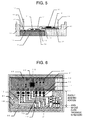
- FIG. 5 is a sectional view of the semiconductor device, the view being taken along line A-A' of FIG. 6,
- FIG. 6 is a top plan view of the semiconductor device before sealing with a resin, and
- FIG. 7 is a circuit diagram of the semiconductor device.
- a main circuit including one or more of power semiconductor elements 11 are composed of a lead frame 13, and an integrated circuit 23, such as a driver IC for driving the power semiconductor elements 11, and a peripheral control circuit part 22 are integrally mounted on a printed circuit board 21.
- the main circuit is provided with an outward guided terminal 17 formed by bending the lead frame 13, the printed circuit board 21 is provided with a control terminal 24, and all mounted parts are housed in a resin-molded outer package and integrally sealed with a resin sealing agent 32.
- the numeral 31 in FIG. 6 indicates a mounting hole.
- the arrangement of the printed circuit board 21 and mounted parts within the semiconductor device is mere a part of the arrangement as a semiconductor device. Therefore, by connecting various printed circuit boards for a power supply portion, control portion, communication portion, display portion, etc. not shown in addition to this arrangement, it is possible to arrange a semiconductor device as a power converter and all the more higher level system.
Landscapes
- Lead Frames For Integrated Circuits (AREA)
- Structures Or Materials For Encapsulating Or Coating Semiconductor Devices Or Solid State Devices (AREA)
Abstract
Description
Claims (3)
- A semiconductor device in which a lead frame (13) fixedly adhered via an insulating layer (18) to one surface of a base substrate (15) serves as a circuit conductor and on which frame one or more of power semiconductor elements (11) are mounted so as to bend an end portion (17) of said lead frame (13) in a stand-up direction from the surface of said base substrate (15) as an outward guided terminal (17),
wherein, in a portion of the lead frame (13), there is formed a recessed portion whose thickness is reduced from the bonding surface of the lead frame (13) to be fixedly adhered to the surface of the base substrate (15) and the lead frame (13) is bent at this recessed portion having a reduced thickness. - A semiconductor device according to claim 1, wherein the stand-up position of the lead frame (13) from the surface of the base substrate (15) may be spaced apart by a predetermined specific distance from an end surface of the base substrate (15).
- A semiconductor device according to claim 2, wherein a curved portion following a straight portion may also be formed in a stand-up portion of the lead frame (13) from the surface of the base substrate (15).
Applications Claiming Priority (2)
| Application Number | Priority Date | Filing Date | Title |
|---|---|---|---|
| JP2000220855A JP2002043496A (en) | 2000-07-21 | 2000-07-21 | Semiconductor device |
| JP2000220855 | 2000-07-21 |
Publications (3)
| Publication Number | Publication Date |
|---|---|
| EP1174921A2 true EP1174921A2 (en) | 2002-01-23 |
| EP1174921A3 EP1174921A3 (en) | 2004-01-02 |
| EP1174921B1 EP1174921B1 (en) | 2006-09-20 |
Family
ID=18715387
Family Applications (1)
| Application Number | Title | Priority Date | Filing Date |
|---|---|---|---|
| EP01305966A Expired - Lifetime EP1174921B1 (en) | 2000-07-21 | 2001-07-11 | Semiconductor device |
Country Status (6)
| Country | Link |
|---|---|
| US (2) | US6541851B2 (en) |
| EP (1) | EP1174921B1 (en) |
| JP (1) | JP2002043496A (en) |
| KR (1) | KR100440416B1 (en) |
| DE (1) | DE60123178T2 (en) |
| TW (1) | TW516200B (en) |
Cited By (4)
| Publication number | Priority date | Publication date | Assignee | Title |
|---|---|---|---|---|
| EP2099121A3 (en) * | 2008-03-04 | 2015-03-11 | Kabushiki Kaisha Toyota Jidoshokki | Power converter apparatus |
| CN108231977A (en) * | 2018-01-09 | 2018-06-29 | 东莞智昊光电科技有限公司 | L ED support and its manufacturing method |
| US20190287884A1 (en) * | 2018-03-13 | 2019-09-19 | Semiconductor Components Industries, Llc | Multi-chip packages with stabilized die pads |
| EP3923321A1 (en) * | 2020-06-08 | 2021-12-15 | CeramTec GmbH | Module with connection tabs for leads |
Families Citing this family (27)
| Publication number | Priority date | Publication date | Assignee | Title |
|---|---|---|---|---|
| JP2002043496A (en) * | 2000-07-21 | 2002-02-08 | Hitachi Ltd | Semiconductor device |
| KR100442847B1 (en) * | 2001-09-17 | 2004-08-02 | 페어차일드코리아반도체 주식회사 | Power semiconductor module that has three dimensional structure and a method of manufacturing thereof |
| JP2003100986A (en) * | 2001-09-26 | 2003-04-04 | Toshiba Corp | Semiconductor device |
| JP4159951B2 (en) * | 2003-09-05 | 2008-10-01 | 三菱電機株式会社 | Manufacturing method of semiconductor module |
| TWI228303B (en) * | 2003-10-29 | 2005-02-21 | Advanced Semiconductor Eng | Semiconductor package, method for manufacturing the same and lead frame for use in the same |
| JP2005191147A (en) * | 2003-12-24 | 2005-07-14 | Sanyo Electric Co Ltd | Method for manufacturing hybrid integrated circuit device |
| JP2006245362A (en) * | 2005-03-04 | 2006-09-14 | Mitsubishi Electric Corp | Semiconductor device and electrode terminal used therefor |
| JP4622646B2 (en) * | 2005-04-19 | 2011-02-02 | 株式会社豊田自動織機 | Semiconductor device |
| JP2007165426A (en) * | 2005-12-12 | 2007-06-28 | Mitsubishi Electric Corp | Semiconductor device |
| US7928540B2 (en) * | 2006-11-10 | 2011-04-19 | Stats Chippac Ltd. | Integrated circuit package system |
| US8139371B2 (en) | 2007-07-30 | 2012-03-20 | GM Global Technology Operations LLC | Power electronics devices with integrated control circuitry |
| US7973433B2 (en) | 2007-07-30 | 2011-07-05 | Nelson David F | Power electronics devices with integrated gate drive circuitry |
| JP5092892B2 (en) * | 2008-05-20 | 2012-12-05 | 株式会社豊田自動織機 | Semiconductor device |
| EP2302674A1 (en) * | 2009-09-29 | 2011-03-30 | ABB Research Ltd. | Electrical terminal, electronic circuit module with an electrical terminal and corresponding method of manufacturing thereof |
| JP2011018933A (en) * | 2010-09-16 | 2011-01-27 | Mitsubishi Electric Corp | Semiconductor device, and method of manufacturing the same |
| CN103370788B (en) * | 2011-04-01 | 2016-10-12 | 富士电机株式会社 | Semiconductor device and manufacture method thereof |
| FI125720B (en) * | 2011-05-19 | 2016-01-29 | Tecnomar Oy | Procedure for the manufacture of electric bridges suitable for roll-to-roll mass production |
| EP2571053A1 (en) | 2011-09-19 | 2013-03-20 | ABB Technology AG | Power semiconductor arrangement and method of forming thereof |
| JP5633496B2 (en) * | 2011-09-29 | 2014-12-03 | 三菱電機株式会社 | Semiconductor device and manufacturing method thereof |
| CN103236422B (en) * | 2013-03-29 | 2015-12-23 | 广东美的制冷设备有限公司 | Intelligent Power Module and manufacture method thereof |
| CN106298553A (en) * | 2015-06-11 | 2017-01-04 | 台达电子企业管理(上海)有限公司 | Packaging module and manufacturing method thereof |
| JP6621714B2 (en) * | 2016-07-01 | 2019-12-18 | 三菱電機株式会社 | Semiconductor device |
| DE202016006849U1 (en) * | 2016-11-07 | 2018-02-08 | Liebherr-Elektronik Gmbh | Power electronics module |
| TWI693682B (en) * | 2019-08-28 | 2020-05-11 | 財團法人工業技術研究院 | Electronic device package structure |
| CN117178643A (en) * | 2021-04-09 | 2023-12-05 | 株式会社村田制作所 | Circuit components including gallium nitride devices |
| JP2023036447A (en) * | 2021-09-02 | 2023-03-14 | 新電元工業株式会社 | Lead frame integrated substrate, semiconductor device, manufacturing method of lead frame integrated substrate, and manufacturing method of semiconductor device |
| KR102834323B1 (en) * | 2022-09-29 | 2025-07-15 | 아이엠에이치(주) | Heat Dissipating Substrate For Semiconductor Device Integrated With Insulation Molding Case And Manufacturing Process Of The Same |
Family Cites Families (10)
| Publication number | Priority date | Publication date | Assignee | Title |
|---|---|---|---|---|
| US4819042A (en) * | 1983-10-31 | 1989-04-04 | Kaufman Lance R | Isolated package for multiple semiconductor power components |
| US4630174A (en) * | 1983-10-31 | 1986-12-16 | Kaufman Lance R | Circuit package with external circuit board and connection |
| JP3120575B2 (en) * | 1992-06-29 | 2000-12-25 | 富士電機株式会社 | Semiconductor device |
| JP3113773B2 (en) | 1994-04-04 | 2000-12-04 | 株式会社日邦バルブ | Air valve |
| JP3309686B2 (en) * | 1995-03-17 | 2002-07-29 | セイコーエプソン株式会社 | Resin-sealed semiconductor device and method of manufacturing the same |
| JPH09129797A (en) * | 1995-10-27 | 1997-05-16 | Hitachi Ltd | Power semiconductor device |
| US6277225B1 (en) * | 1996-03-13 | 2001-08-21 | Micron Technology, Inc. | Stress reduction feature for LOC lead frame |
| JPH11142663A (en) | 1997-11-06 | 1999-05-28 | Nippon Telegr & Teleph Corp <Ntt> | Magneto-optical waveguide and method of manufacturing the same |
| JP3674333B2 (en) * | 1998-09-11 | 2005-07-20 | 株式会社日立製作所 | Power semiconductor module and electric motor drive system using the same |
| JP2002043496A (en) * | 2000-07-21 | 2002-02-08 | Hitachi Ltd | Semiconductor device |
-
2000
- 2000-07-21 JP JP2000220855A patent/JP2002043496A/en active Pending
-
2001
- 2001-07-06 TW TW090116646A patent/TW516200B/en active
- 2001-07-11 EP EP01305966A patent/EP1174921B1/en not_active Expired - Lifetime
- 2001-07-11 DE DE60123178T patent/DE60123178T2/en not_active Expired - Lifetime
- 2001-07-20 KR KR10-2001-0043876A patent/KR100440416B1/en not_active Expired - Fee Related
- 2001-07-20 US US09/908,564 patent/US6541851B2/en not_active Expired - Fee Related
-
2003
- 2003-03-11 US US10/384,731 patent/US6720646B2/en not_active Expired - Lifetime
Cited By (6)
| Publication number | Priority date | Publication date | Assignee | Title |
|---|---|---|---|---|
| EP2099121A3 (en) * | 2008-03-04 | 2015-03-11 | Kabushiki Kaisha Toyota Jidoshokki | Power converter apparatus |
| CN108231977A (en) * | 2018-01-09 | 2018-06-29 | 东莞智昊光电科技有限公司 | L ED support and its manufacturing method |
| US20190287884A1 (en) * | 2018-03-13 | 2019-09-19 | Semiconductor Components Industries, Llc | Multi-chip packages with stabilized die pads |
| EP3923321A1 (en) * | 2020-06-08 | 2021-12-15 | CeramTec GmbH | Module with connection tabs for leads |
| EP3923322A1 (en) * | 2020-06-08 | 2021-12-15 | CeramTec GmbH | Module with connection tabs for leads |
| US11631636B2 (en) | 2020-06-08 | 2023-04-18 | Ceramtec Gmbh | Module with connection lugs for supply lines |
Also Published As
| Publication number | Publication date |
|---|---|
| JP2002043496A (en) | 2002-02-08 |
| US20020008312A1 (en) | 2002-01-24 |
| KR20020009449A (en) | 2002-02-01 |
| US6720646B2 (en) | 2004-04-13 |
| US6541851B2 (en) | 2003-04-01 |
| DE60123178D1 (en) | 2006-11-02 |
| TW516200B (en) | 2003-01-01 |
| EP1174921A3 (en) | 2004-01-02 |
| KR100440416B1 (en) | 2004-07-21 |
| DE60123178T2 (en) | 2007-10-25 |
| EP1174921B1 (en) | 2006-09-20 |
| US20030146501A1 (en) | 2003-08-07 |
Similar Documents
| Publication | Publication Date | Title |
|---|---|---|
| EP1174921B1 (en) | Semiconductor device | |
| US6297074B1 (en) | Film carrier tape and laminated multi-chip semiconductor device incorporating the same and method thereof | |
| EP3226292B1 (en) | Lead frame, semiconductor device, method for manufacturing lead frame, and method for manufacturing semiconductor device | |
| KR101037997B1 (en) | A semiconductor die package and a substrate for a semiconductor die package, a method of forming the same, and a manufacturing method and processing method of a lead frame structure | |
| US20110108964A1 (en) | Semiconductor device and manufacturing method thereof | |
| GB2317989A (en) | Lead frames for semiconductor packages | |
| US5528458A (en) | Integrated circuit device and its manufacturing method | |
| JPH08306855A (en) | Semiconductor package, lead frame, circuit board, semiconductor package molding die, electronic circuit board, and lead frame manufacturing method | |
| CN112490234B (en) | Intelligent power module and manufacturing method of intelligent power module | |
| CN214705926U (en) | Intelligent power module | |
| US20090035896A1 (en) | High power mcm package with improved planarity and heat dissipation | |
| JP2720008B2 (en) | Power semiconductor module | |
| JP2001358263A (en) | Semiconductor device and circuit forming method thereof | |
| US6905361B2 (en) | Electrical device | |
| CN112490233A (en) | Intelligent power module and manufacturing method thereof | |
| EP3761358A1 (en) | A lead frame assembly for a semiconductor device | |
| JPH0661372A (en) | Hybrid IC | |
| CN214705927U (en) | Smart Power Module | |
| US20040119155A1 (en) | Metal wiring board and method for manufacturing the same | |
| JP2954112B2 (en) | BGA type semiconductor device and manufacturing method thereof | |
| JP2536568B2 (en) | Lead frame | |
| JPH06140535A (en) | Tape carrier package type semiconductor device | |
| JP2504262Y2 (en) | Semiconductor module | |
| JPS5923432Y2 (en) | semiconductor equipment | |
| CN119764277A (en) | Surface Mount Modules |
Legal Events
| Date | Code | Title | Description |
|---|---|---|---|
| PUAI | Public reference made under article 153(3) epc to a published international application that has entered the european phase |
Free format text: ORIGINAL CODE: 0009012 |
|
| 17P | Request for examination filed |
Effective date: 20010731 |
|
| AK | Designated contracting states |
Kind code of ref document: A2 Designated state(s): AT BE CH CY DE DK ES FI FR GB GR IE IT LI LU MC NL PT SE TR |
|
| AX | Request for extension of the european patent |
Free format text: AL;LT;LV;MK;RO;SI |
|
| PUAL | Search report despatched |
Free format text: ORIGINAL CODE: 0009013 |
|
| AK | Designated contracting states |
Kind code of ref document: A3 Designated state(s): AT BE CH CY DE DK ES FI FR GB GR IE IT LI LU MC NL PT SE TR |
|
| AX | Request for extension of the european patent |
Extension state: AL LT LV MK RO SI |
|
| RIC1 | Information provided on ipc code assigned before grant |
Ipc: 7H 01L 23/495 A Ipc: 7H 01L 25/07 B |
|
| AKX | Designation fees paid |
Designated state(s): DE FR GB |
|
| 17Q | First examination report despatched |
Effective date: 20050610 |
|
| GRAP | Despatch of communication of intention to grant a patent |
Free format text: ORIGINAL CODE: EPIDOSNIGR1 |
|
| GRAS | Grant fee paid |
Free format text: ORIGINAL CODE: EPIDOSNIGR3 |
|
| GRAA | (expected) grant |
Free format text: ORIGINAL CODE: 0009210 |
|
| AK | Designated contracting states |
Kind code of ref document: B1 Designated state(s): DE FR GB |
|
| REG | Reference to a national code |
Ref country code: GB Ref legal event code: FG4D |
|
| REF | Corresponds to: |
Ref document number: 60123178 Country of ref document: DE Date of ref document: 20061102 Kind code of ref document: P |
|
| ET | Fr: translation filed | ||
| PLBI | Opposition filed |
Free format text: ORIGINAL CODE: 0009260 |
|
| PLAX | Notice of opposition and request to file observation + time limit sent |
Free format text: ORIGINAL CODE: EPIDOSNOBS2 |
|
| 26 | Opposition filed |
Opponent name: INFINEON TECHNOLOGIES AG Effective date: 20070620 |
|
| PLBB | Reply of patent proprietor to notice(s) of opposition received |
Free format text: ORIGINAL CODE: EPIDOSNOBS3 |
|
| PLAB | Opposition data, opponent's data or that of the opponent's representative modified |
Free format text: ORIGINAL CODE: 0009299OPPO |
|
| PLCK | Communication despatched that opposition was rejected |
Free format text: ORIGINAL CODE: EPIDOSNREJ1 |
|
| APAH | Appeal reference modified |
Free format text: ORIGINAL CODE: EPIDOSCREFNO |
|
| APBM | Appeal reference recorded |
Free format text: ORIGINAL CODE: EPIDOSNREFNO |
|
| APBP | Date of receipt of notice of appeal recorded |
Free format text: ORIGINAL CODE: EPIDOSNNOA2O |
|
| APBQ | Date of receipt of statement of grounds of appeal recorded |
Free format text: ORIGINAL CODE: EPIDOSNNOA3O |
|
| PLAB | Opposition data, opponent's data or that of the opponent's representative modified |
Free format text: ORIGINAL CODE: 0009299OPPO |
|
| R26 | Opposition filed (corrected) |
Opponent name: INFINEON TECHNOLOGIES AG Effective date: 20070620 |
|
| APBY | Invitation to file observations in appeal sent |
Free format text: ORIGINAL CODE: EPIDOSNOBA2O |
|
| REG | Reference to a national code |
Ref country code: FR Ref legal event code: PLFP Year of fee payment: 16 |
|
| APBU | Appeal procedure closed |
Free format text: ORIGINAL CODE: EPIDOSNNOA9O |
|
| REG | Reference to a national code |
Ref country code: DE Ref legal event code: R100 Ref document number: 60123178 Country of ref document: DE |
|
| PGFP | Annual fee paid to national office [announced via postgrant information from national office to epo] |
Ref country code: FR Payment date: 20160613 Year of fee payment: 16 |
|
| PGFP | Annual fee paid to national office [announced via postgrant information from national office to epo] |
Ref country code: GB Payment date: 20160706 Year of fee payment: 16 Ref country code: DE Payment date: 20160705 Year of fee payment: 16 |
|
| PLAG | Information modified related to despatch of communication that opposition is rejected |
Free format text: ORIGINAL CODE: EPIDOSCREJ1 |
|
| REG | Reference to a national code |
Ref country code: DE Ref legal event code: R119 Ref document number: 60123178 Country of ref document: DE |
|
| GBPC | Gb: european patent ceased through non-payment of renewal fee |
Effective date: 20170711 |
|
| REG | Reference to a national code |
Ref country code: FR Ref legal event code: ST Effective date: 20180330 |
|
| PG25 | Lapsed in a contracting state [announced via postgrant information from national office to epo] |
Ref country code: GB Free format text: LAPSE BECAUSE OF NON-PAYMENT OF DUE FEES Effective date: 20170711 Ref country code: DE Free format text: LAPSE BECAUSE OF NON-PAYMENT OF DUE FEES Effective date: 20180201 |
|
| PG25 | Lapsed in a contracting state [announced via postgrant information from national office to epo] |
Ref country code: FR Free format text: LAPSE BECAUSE OF NON-PAYMENT OF DUE FEES Effective date: 20170731 |
|
| PLBN | Opposition rejected |
Free format text: ORIGINAL CODE: 0009273 |
|
| STAA | Information on the status of an ep patent application or granted ep patent |
Free format text: STATUS: OPPOSITION REJECTED |
|
| 27O | Opposition rejected |
Effective date: 20160622 |