EP1172850A2 - Semiconductor device having at least three power terminals superposed on each other - Google Patents
Semiconductor device having at least three power terminals superposed on each other Download PDFInfo
- Publication number
- EP1172850A2 EP1172850A2 EP01115799A EP01115799A EP1172850A2 EP 1172850 A2 EP1172850 A2 EP 1172850A2 EP 01115799 A EP01115799 A EP 01115799A EP 01115799 A EP01115799 A EP 01115799A EP 1172850 A2 EP1172850 A2 EP 1172850A2
- Authority
- EP
- European Patent Office
- Prior art keywords
- power terminal
- power
- power terminals
- semiconductor device
- terminals
- Prior art date
- Legal status (The legal status is an assumption and is not a legal conclusion. Google has not performed a legal analysis and makes no representation as to the accuracy of the status listed.)
- Withdrawn
Links
Images


Classifications
-
- H—ELECTRICITY
- H10—SEMICONDUCTOR DEVICES; ELECTRIC SOLID-STATE DEVICES NOT OTHERWISE PROVIDED FOR
- H10W—GENERIC PACKAGES, INTERCONNECTIONS, CONNECTORS OR OTHER CONSTRUCTIONAL DETAILS OF DEVICES COVERED BY CLASS H10
- H10W90/00—Package configurations
-
- H—ELECTRICITY
- H10—SEMICONDUCTOR DEVICES; ELECTRIC SOLID-STATE DEVICES NOT OTHERWISE PROVIDED FOR
- H10W—GENERIC PACKAGES, INTERCONNECTIONS, CONNECTORS OR OTHER CONSTRUCTIONAL DETAILS OF DEVICES COVERED BY CLASS H10
- H10W44/00—Electrical arrangements for controlling or matching impedance
- H10W44/501—Inductive arrangements
-
- H—ELECTRICITY
- H10—SEMICONDUCTOR DEVICES; ELECTRIC SOLID-STATE DEVICES NOT OTHERWISE PROVIDED FOR
- H10W—GENERIC PACKAGES, INTERCONNECTIONS, CONNECTORS OR OTHER CONSTRUCTIONAL DETAILS OF DEVICES COVERED BY CLASS H10
- H10W90/00—Package configurations
- H10W90/701—Package configurations characterised by the relative positions of pads or connectors relative to package parts
- H10W90/731—Package configurations characterised by the relative positions of pads or connectors relative to package parts of die-attach connectors
- H10W90/736—Package configurations characterised by the relative positions of pads or connectors relative to package parts of die-attach connectors between a chip and a stacked lead frame, conducting package substrate or heat sink
-
- H—ELECTRICITY
- H10—SEMICONDUCTOR DEVICES; ELECTRIC SOLID-STATE DEVICES NOT OTHERWISE PROVIDED FOR
- H10W—GENERIC PACKAGES, INTERCONNECTIONS, CONNECTORS OR OTHER CONSTRUCTIONAL DETAILS OF DEVICES COVERED BY CLASS H10
- H10W90/00—Package configurations
- H10W90/701—Package configurations characterised by the relative positions of pads or connectors relative to package parts
- H10W90/751—Package configurations characterised by the relative positions of pads or connectors relative to package parts of bond wires
- H10W90/753—Package configurations characterised by the relative positions of pads or connectors relative to package parts of bond wires between laterally-adjacent chips
-
- H—ELECTRICITY
- H10—SEMICONDUCTOR DEVICES; ELECTRIC SOLID-STATE DEVICES NOT OTHERWISE PROVIDED FOR
- H10W—GENERIC PACKAGES, INTERCONNECTIONS, CONNECTORS OR OTHER CONSTRUCTIONAL DETAILS OF DEVICES COVERED BY CLASS H10
- H10W90/00—Package configurations
- H10W90/701—Package configurations characterised by the relative positions of pads or connectors relative to package parts
- H10W90/751—Package configurations characterised by the relative positions of pads or connectors relative to package parts of bond wires
- H10W90/754—Package configurations characterised by the relative positions of pads or connectors relative to package parts of bond wires between a chip and a stacked insulating package substrate, interposer or RDL
Definitions
- the present invention relates to a semiconductor device for large power, such as IGBT module. Also, the invention is applied to the structure of semiconductor device required to reduce the power loss.
- a structure, as shown in FIG. 9 for instance, is known as an example of semiconductor device for large power according to the prior art.
- this example relates to the structure of IGBT module.
- FIG. 9A a collector side of an IGBT chip 65 and an n layer side of a diode chip 66 are soldered respectively, on a Cu pattern 63 of the surface of a DBC (Direct Bond Copper) substrate wherein copper conductors sandwich an insulation substrate 67 of alumina.
- An emitter side of the IGBT chip 65 and a p layer side of the diode chip 66 are connected with an external power terminal 61, through an Al bonding wire of, for example, 200 to 500 ⁇ m ⁇ , extending from both chips.
- the surface Cu pattern 63 is connected to an external power terminal 62.
- Such structure is place on a heat radiation plate 69.
- a gate terminal 70 shown in FIG. 9B is not illustrated.
- the external power terminal 61 is connected with the chip 65, 66 through the bonding wire 64. Consequently, wiring resistance caused by the bonding wire 64 and self-inductance increase inconveniently.
- the present invention is devised considering problems of the aforementioned structure, and has an object of providing a semiconductor device for large power, such as IGBT module, reducing a wiring resistance caused by the wiring metal such as bonding wire, and self-inductance, and further improving the heat diffusion.
- the present invention relates to a structure for reducing a wiring resistance caused by the wiring metal such as bonding wire, and self-inductance, and further improving the heat diffusion, and is a semiconductor device having at least three or more power terminals superimposed on each other, at least one semiconductor chip arranged in a way sandwiched between two predetermined power terminals among the power terminals, wherein the two power terminals and the semiconductor chip are connected electrically each other.
- electrodes and Cu patterns or the like on the IGBT chip and diode chip are connected electrically to the external power terminal through bonding wire.
- the number of bonding wires is increased to respond to the required large current.
- bonding wires each having a certain length are used, the resistance of bonding wires and the self-inductance caused by their length increase.
- the invention is for connecting directly the IGBT chip and the external power terminal as shown in FIG. 1B for example, in order to solve the problem of increase of bonding wire resistance and inductance.
- it is proposed to provide a specific structure for reducing resistance component produced by the use of bonding wire and self-inductance component.
- a structure for flowing current inversely is adopted.
- Such a structure allows to reduce the inductance by the mutual inductance effect.
- the adoption of a structure allowing to use the external power terminal as heat radiation plate realizes the reduction of heat resistance by avoiding to use as separate heat radiation plate and the cost reduction by eliminating a part.
- the invention intends to reduce the resistance and the inductance of power wiring portion, and cut the cost, by connecting external power terminals directly to the top face electrode and the bottom face electrode of an IGTB chip.
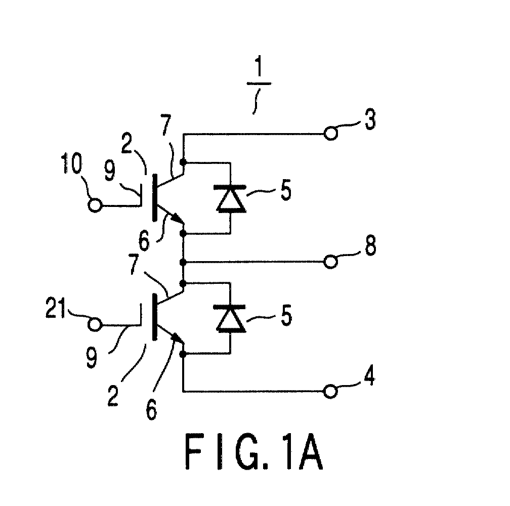
- FIG. 1A shows a IGBT module 1 having a half bridge configuration, which is a first embodiment of the present invention.
- the a circuit diagram of this IGBT module 1 is shown in FIG. 1A
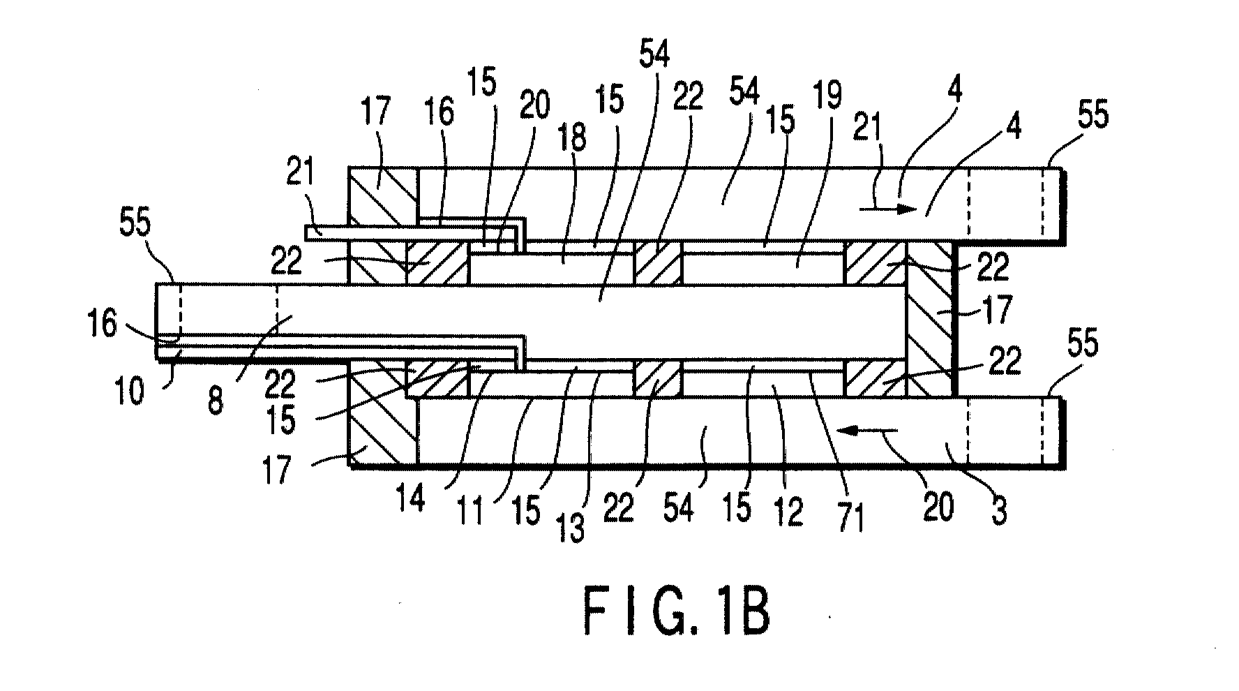
- a schematic section view of this IGBT module is shown in FIG. 1B
- a plan view showing the schematic configuration of this IGBT module inside is shown in FIG. 1C.
- IGBT half bridge circuit shown in FIG. 1A, two IGBT elements 2 are connected in series and a collector 7 of one IGBT element and an emitter of the other IGBT element are connected respectively to a first and a second external power elements 3, 4.
- diodes 5 are connected respectively in parallel to the emitter 6 and the collector 7 of respective IGBT elements.
- a relay power terminal 8 which is third external power element is connected between two IGBT elements.
- Control terminals 10, 21 are connected respectively to a gate of two IGBT elements 2.
- FIG. 1B and FIG. 1C The structure of this IGBT module is shown in FIG. 1B and FIG. 1C.
- a collector side electrode of a first IGBT chip 11 and a n layer side electrode of the first diode chip 12 are connected to a first external power terminal 3 of the lower part by soldering or the other methods.
- a metal film is formed on each electrode in order to facilitate a connection.
- both electrodes can be adhered using, for instance, a conductive resin.
- an insulator layer 22 made, for example, of polyimide resin, epoxy resin or the like, may be arranged around the IGBT chip 11 and the diode chip 12 for securing a mutual insulation of the IGBT chip 11 and the diode chip 12.
- Copper or copper alloys excellent in heat conductivity and electric conductivity are used in general, for the external power terminals 3, 4 and the relay power terminal 8, and DBC substrate is used as necessary. These terminals function also as heat diffusion member for diffusing head generated in respective chips.
- a metal film is formed on an emitter surface 13 of the aforementioned IGBT chip 11 and a p layer surface 71 of the diode chip 12 for facilitating the electric connection.
- the relay power terminal 8 is connected to the semiconductor chip by soldering or other methods, through a buffer plate 15 of molybdenum thin plate or the like, for example, to buffer the stress generated between the semiconductor chip and the electric terminals. Copper or copper alloys are used also for the relay power terminal 8 as for the first external power terminal, and DBC substrate is used as necessary.
- a control terminal 10 is also connected to a gate surface 14 of the IGBT chip 11, similarly through a buffer plate 15. It is preferable to form this control terminal in a molded resin holder 17 constituting a housing for the IGBT module 1. As necessary, an insulation layer 16 is provided between the relay power terminal 8 and the control terminal 10. As the other structure, it is also possible to connect the control terminal 10 and the gate surface 14 by wire bonding (refer to control terminal 38 and bonding wire 39 in FIG. 3).
- At least the external power terminal 3 and the external power terminal 4 are arranged in parallel and opposed to each other, and disposed so that the current flowing in respective external power terminals 3, 4 flows in the opposite direction.
- a control terminal 21 is also connected to a gate surface 20 of a second IGBT chip 18 by soldering, bonding or other methods.
- FIG. 1B shows an example of connecting the control terminal 21 by soldering, it may also be connected by wire bonding similarly as the control terminal 10 of the first IGBT chip 11.
- an insulation layer 16 is provided between the second external power terminal 4 and the control terminal 21. The assembling operation can be facilitated by forming also this control terminal 21 in the resin holder 17 beforehand.
- an insulator layer 22 made, for example, of polyimide resin, epoxy resin or the like, around the IGBT chips 11, 18 and the diode chips 12, 19 for securing a mutual insulation between chips and between electrodes.
- FIG. 1C shows a plan view of the module inside.
- the second external power terminal 4 is constituted to cover entirely an emitter electrode 23 of the second IGBT chip 18 and a p layer side electrode 24 of the second diode chip 19.
- a through hole 71 is formed in the second external power terminal 4 and relay power terminal 8 for connecting with the power terminal of a power apparatus using this IGTB module.
- a external power terminal 3 (not shown) may also have a similar structure.
- the relay power terminal 8 can be made to function as heat radiation plate, thereby making it unnecessary to connect additionally a new another heat radiation plate, allowing, therefore, to intend to reduce the number of processes during assembling or use of the module, and to cut the cost.
- the insulation substrate for electric wiring layout is not required, thereby making it unnecessary to use an insulation substrate of lower heat conductivity than the metal, and a low heat resistance can be realized.
- FIG. 2 shows an IGBT module 25 of 6in1 structure which is a second embodiment of the invention.
- FIG. 2A shows the circuit diagram of an IGBT module
- FIG. 2B shows the module inside plan view.
- a single module is constituted by connecting in parallel three circuits of IGBT module of the first embodiment.
- Three upper IGTB 26 are arranged on three lower IGBT 28, and upper and lower IGBT 26, 27 are connected respectively in series, forming a three phased structure.
- three upper diodes 27 are arranged on three lower diodes 29, and upper and lower diodes are connected in parallel respectively to the corresponding IGBT.
- Respective phase is bound respectively to the first external power terminal 30 and the second external power terminal 31 integrating three phases.
- a relay power terminal 32 is formed at the junction of upper and lower elements of each phase, and control terminals 33, 34 to be connected to the gate of each IGBT 26, 27 are formed.
- the internal structure is similar to the first embodiment shown in FIG. 1B and FIG. 1C, but an insulation layer 35 can be provided for securing insulation between respective phases.
- a resin holder 36 forms a housing for the module 25.
- the second embodiment can realize the simplification of structure and the miniaturization of apparatus in a case of using as three-phased module, in addition to the effects mentioned for the first embodiment.
- FIG. 3 shows the inside plan view of a third embodiment modifying the structure of the control terminals 21, 10 and the second external power terminal 4 of the first embodiment. It is different from the first embodiment in that a structure for connecting an IGBT chip 37 and a control terminal 38 by a bonding wire 39 (or soldering) and taking out the control terminal 38 from the center of a module 40. As necessary, it is also possible to constitute to bring a signal system emitter terminal 41 near the control terminal 38 and to output directly from the external power terminal 4. Such a configuration makes easy to bound the control apparatus with the control system circuit, especially to dispose the wiring, in a case of using the IGBT module for power control apparatus or others.
- Adopting such a configuration a structure that can realize a still lower resistance and a still lower inductance can be made, because the distance between the IGBT chip 37 and the external connection position of the second external power terminal 4 becomes still shorter. As necessary, it is also possible to arrange the signal system emitter 41 near the control terminal 38.
- the fifth embodiment modifies the layout of the relay power terminal 8 of the first embodiment.
- the inside plan view of the fifth embodiment is shown in FIG. 5. It is different from the first embodiment in that the leading out direction of the relay power terminal 8 is perpendicular to the leading out direction of the second external power terminal 4.
- the distance between the relay power terminal 8 and the external power terminal 45 becomes shorter, allowing to intend to reduce the electric resistance between the external power terminal 45 and the relay power terminal 8.
- FIG. 6 shows the structure of a sixth embodiment.
- the sixth embodiment is for dividing the second external power terminal 31 of the second embodiment shown in FIG. 2 and a first external power terminal (not shown) respectively into three phases.
- FIG. 6 shows the inside plan thereof. It is different from the second example in that, as mentioned above, the second external power terminal 31 of FIG. 2 (similar for the first external power terminal) is divided into three eternal power terminals 44 to 46 for each phase.
- Adopting such configuration it becomes possible to intend to miniaturize the module portion and to reduce the number of processes of assembling, in an application of simply using and arranging three IGBT modules 1 of the first embodiment in parallel. Therefore, it can be intended to cut the cost of the module portion.
- FIG. 7 shows an embodiment in a case of adopting the pressure welding for respective semiconductor chips and respective power terminals of the first example, in place of connection by soldering.
- FIG. 7A shows a case of connecting by pressure welding 47 both faces of the IGBT chip and diode chips
- FIG. 7B shows a case of connecting by pressure welding 47 only one face of each chip, and the other face by soldering 42.
- FIG. 7C shows the inside plan view of a case of adopting the pressure welding connection.
- the seventh embodiment has a structure of laminating in order an external power terminal 4, a buffer plate 15, semiconductor chips 18, 19 such as IGBT, diode or the like wherein an aluminum electrode is formed by deposition or others, for instance, as pressure welding face, a relay power terminal 8, a buffer plate 15 made, for example, of a molybdenum plate, semiconductor chips 11, 12, and an external power terminal 3.
- FIG. 7A A structure wherein both electrode faces of the semiconductor chip are connected by pressure welding 47 is shown in FIG. 7A.
- a structure wherein the electrode face of one side of respective semiconductor chips is connected by pressure welding 47 and the other face is connected by soldering is shown in FIG. 7B.
- FIG. 8A shows a configuration for inverting the polarity of one IGBT 52 (upside in the drawing) of two IGBTs of the first embodiment. According to this inversion, the diode 73 of the corresponding side is also inverted. Then, the emitter of one IGBT 52 is connected to the fourth power terminal, and the emitter of the other IGBT 53 is connected to the fifth power terminal, both collectors 7 are connected mutually for connecting with a mutual power terminal 51.
- FIG. 8A shows the circuit diagram
- FIG. 8B shows the sectional structure drawing thereof.
- This configuration has an advantage of facilitating the parallel connection of two IGBT elements 52, 53, and increasing the power by such a connection, by connecting the fourth power terminal 49 and the fifth power terminal 50.
Landscapes
- Inverter Devices (AREA)
- Power Conversion In General (AREA)
- Lead Frames For Integrated Circuits (AREA)
Abstract
Description
Claims (10)
- A semiconductor device characterized by comprising at least three or more power terminals (3, 4, 8) superimposed on each other, and at least one semiconductor chip (2, 5) is connected electrically in a way to be sandwiched between predetermined two power terminals (3, 8 or 4, 8) among said power terminals, in a semiconductor device for large power.
- The semiconductor device according to claim 1, characterized in that a power terminal on one end among said superposed power terminals (3, 4, 8) and a power terminal (3, 4) on the other end among said superposed power terminals are led out in the same direction.
- The semiconductor device according to claim 2, characterized in that a power terminal (8) positioned at the middle among said superposed power terminals (3, 4, 8) is led out in a direction opposite to or perpendicular to a power terminal (3, 4) on said one or other end.
- The semiconductor device according to claim 1, characterized in that one face of said at least one semiconductor chip (2, 5) sandwiched between said two power terminals is connected to one power terminal of said two power terminals by soldering or pressure welding, and the other face is connected to the other power terminal of said two power terminals by soldering or pressure welding through a buffer plate (15).
- The semiconductor device according to claim 1, characterized in that said at least one semiconductor chip (2, 5) operates, so that the current flows in the opposite direction for the power terminal on one end among said superposed power terminals (3, 4, 8) and for the power terminal (3, 4) on the other end.
- The semiconductor device according to claim 1, characterized in that said at least one semiconductor chip sandwiched between said power terminals is made of a plurality of semiconductor chips (2, 5), and an insulation layer (22) is provided among said semiconductor chips.
- The semiconductor device according to claim 6, characterized in that said plurality of semiconductor chips comprises at least one transistor (2), and at least diode (5), and a control electrode (38) is connected to said transistor
- The semiconductor device according to claim 7, characterized in that said control electrode (38) and a control electrode pad of said transistor (2) are connected by wire bonding (39), or connected directly by sandwiching a buffer plate.
- The semiconductor device according to claim 7, characterized in that said control electrode (38) is led out in a direction opposite to or perpendicular to a power terminal (4, 8) positioned on one end of said power terminal or on the other end of said power terminal.
- The semiconductor device according to claim 4, characterized in that the power terminals (4, 8) positioned on one end of said power terminal and the power terminal on the other end have a screw fixing structure (48) so as to connect semiconductor chips by pressure welding between any two power terminals of said power terminals superimposed on each other.
Applications Claiming Priority (2)
| Application Number | Priority Date | Filing Date | Title |
|---|---|---|---|
| JP2000210475A JP2002026251A (en) | 2000-07-11 | 2000-07-11 | Semiconductor device |
| JP2000210475 | 2000-07-11 |
Publications (2)
| Publication Number | Publication Date |
|---|---|
| EP1172850A2 true EP1172850A2 (en) | 2002-01-16 |
| EP1172850A3 EP1172850A3 (en) | 2006-04-26 |
Family
ID=18706739
Family Applications (1)
| Application Number | Title | Priority Date | Filing Date |
|---|---|---|---|
| EP20010115799 Withdrawn EP1172850A3 (en) | 2000-07-11 | 2001-07-11 | Semiconductor device having at least three power terminals superposed on each other |
Country Status (6)
| Country | Link |
|---|---|
| US (1) | US6885096B2 (en) |
| EP (1) | EP1172850A3 (en) |
| JP (1) | JP2002026251A (en) |
| KR (1) | KR100430772B1 (en) |
| CN (1) | CN1204623C (en) |
| TW (1) | TW498550B (en) |
Cited By (13)
| Publication number | Priority date | Publication date | Assignee | Title |
|---|---|---|---|---|
| FR2842352A1 (en) * | 2002-07-15 | 2004-01-16 | Mitsubishi Electric Corp | POWER SEMICONDUCTOR DEVICE |
| EP1411551A1 (en) * | 2002-10-16 | 2004-04-21 | Nissan Motor Co., Ltd. | Stacked semiconductor module and assembling method of the same |
| EP1469515A2 (en) * | 2003-04-02 | 2004-10-20 | HILL, Wolfgang | Power stage to drive an electric machine |
| EP1484797A1 (en) * | 2003-06-04 | 2004-12-08 | Alstom | Inverter power device and method of making it |
| WO2006078070A3 (en) * | 2005-01-24 | 2006-10-19 | Toyota Motor Co Ltd | Semiconductor module and semiconductor device |
| EP1855374A3 (en) * | 2006-04-27 | 2008-07-16 | Hitachi, Ltd. | Electric circuit device, electric circuit module, and power converter |
| WO2009062534A1 (en) * | 2007-11-13 | 2009-05-22 | Siemens Aktiengesellschaft | Power semiconductor module |
| EP1657750A4 (en) * | 2003-08-18 | 2009-09-02 | Sanken Electric Co Ltd | SEMICONDUCTOR DEVICE |
| EP2413680A4 (en) * | 2009-03-26 | 2013-05-29 | Panasonic Corp | ELECTRONIC DEVICE ON BOARD VEHICLE |
| WO2015043795A3 (en) * | 2013-09-24 | 2015-07-16 | Conti Temic Microelectronic Gmbh | Power module, power converter, and drive arrangement having a power module |
| EP2579439A3 (en) * | 2008-03-11 | 2015-09-09 | Hitachi Ltd. | Electric power conversion apparatus |
| CN107851634A (en) * | 2015-05-22 | 2018-03-27 | Abb瑞士股份有限公司 | Power semiconductor modular |
| DE102017109515B4 (en) | 2017-05-04 | 2024-10-02 | Schaeffler Technologies AG & Co. KG | Semiconductor device and method for its manufacture |
Families Citing this family (62)
| Publication number | Priority date | Publication date | Assignee | Title |
|---|---|---|---|---|
| EP1148547B8 (en) | 2000-04-19 | 2016-01-06 | Denso Corporation | Coolant cooled type semiconductor device |
| JP4323299B2 (en) * | 2003-12-03 | 2009-09-02 | 三菱電機株式会社 | Semiconductor device |
| DE102004027185B4 (en) * | 2004-06-03 | 2008-08-28 | Infineon Technologies Ag | Low-inductance semiconductor device with half-bridge configuration |
| JP4743396B2 (en) * | 2004-07-29 | 2011-08-10 | ヤマハ発動機株式会社 | Power module, motor control unit, electric transport device, and method of manufacturing power module |
| JP4478049B2 (en) * | 2005-03-15 | 2010-06-09 | 三菱電機株式会社 | Semiconductor device |
| JP4552810B2 (en) * | 2005-09-06 | 2010-09-29 | 株式会社デンソー | Semiconductor device |
| TWI302813B (en) * | 2006-01-11 | 2008-11-01 | Via Tech Inc | Circuit board and electronic assembly |
| US8129836B2 (en) | 2006-06-09 | 2012-03-06 | Honda Motor Co., Ltd. | Semiconductor device |
| JP4829690B2 (en) * | 2006-06-09 | 2011-12-07 | 本田技研工業株式会社 | Semiconductor device |
| JP5232367B2 (en) * | 2006-07-12 | 2013-07-10 | ルネサスエレクトロニクス株式会社 | Semiconductor device |
| JP4820233B2 (en) * | 2006-08-09 | 2011-11-24 | 本田技研工業株式会社 | Semiconductor device |
| EP2051301A4 (en) | 2006-08-09 | 2010-06-16 | Honda Motor Co Ltd | SEMICONDUCTOR DEVICE |
| TWI315567B (en) * | 2006-11-10 | 2009-10-01 | Via Tech Inc | Electronic assembly and circuit board |
| JP5227532B2 (en) * | 2007-04-02 | 2013-07-03 | 日立オートモティブシステムズ株式会社 | Semiconductor module for inverter circuit |
| JP2009043820A (en) | 2007-08-07 | 2009-02-26 | Rohm Co Ltd | High efficiency module |
| US7773381B2 (en) | 2007-09-26 | 2010-08-10 | Rohm Co., Ltd. | Semiconductor device |
| JP5092654B2 (en) * | 2007-09-28 | 2012-12-05 | 株式会社デンソー | Power converter |
| JP5067267B2 (en) | 2008-06-05 | 2012-11-07 | 三菱電機株式会社 | Resin-sealed semiconductor device and manufacturing method thereof |
| JP5253430B2 (en) * | 2009-03-23 | 2013-07-31 | 株式会社豊田中央研究所 | Power module |
| US9147666B2 (en) | 2009-05-14 | 2015-09-29 | Rohm Co., Ltd. | Semiconductor device |
| JP5481148B2 (en) * | 2009-10-02 | 2014-04-23 | 日立オートモティブシステムズ株式会社 | Semiconductor device, power semiconductor module, and power conversion device including power semiconductor module |
| FR2951019B1 (en) * | 2009-10-07 | 2012-06-08 | Valeo Etudes Electroniques | POWER MODULE FOR MOTOR VEHICLE |
| JP5581724B2 (en) * | 2010-02-22 | 2014-09-03 | ダイキン工業株式会社 | Power converter |
| US8513784B2 (en) * | 2010-03-18 | 2013-08-20 | Alpha & Omega Semiconductor Incorporated | Multi-layer lead frame package and method of fabrication |
| JP5494147B2 (en) * | 2010-04-06 | 2014-05-14 | 富士電機株式会社 | Power semiconductor module and power converter using the same |
| JP5440335B2 (en) | 2010-04-06 | 2014-03-12 | 富士電機株式会社 | Power semiconductor module and power converter using the same |
| JP5242629B2 (en) * | 2010-05-10 | 2013-07-24 | 株式会社東芝 | Power semiconductor device |
| US9704831B2 (en) | 2010-05-21 | 2017-07-11 | Mitsubishi Electric Corporation | Power semiconductor module |
| JP2010258485A (en) * | 2010-08-24 | 2010-11-11 | Renesas Electronics Corp | Semiconductor device |
| JP5846123B2 (en) | 2010-11-29 | 2016-01-20 | トヨタ自動車株式会社 | Power module |
| US8963338B2 (en) * | 2011-03-02 | 2015-02-24 | International Rectifier Corporation | III-nitride transistor stacked with diode in a package |
| JP5387620B2 (en) * | 2011-05-31 | 2014-01-15 | 株式会社安川電機 | Power conversion device, semiconductor device, and method of manufacturing power conversion device |
| US8987777B2 (en) * | 2011-07-11 | 2015-03-24 | International Rectifier Corporation | Stacked half-bridge power module |
| JP2012074730A (en) * | 2011-12-07 | 2012-04-12 | Mitsubishi Electric Corp | Power semiconductor module |
| CN102857078A (en) * | 2012-01-05 | 2013-01-02 | 中国电力科学研究院 | Convertor unit based on welding type insulated gate bipolar transistor (IGBT) and pressure welding type diode antiparallel structure |
| JPWO2013121691A1 (en) * | 2012-02-14 | 2015-05-11 | パナソニックIpマネジメント株式会社 | Semiconductor device |
| ITMI20120713A1 (en) | 2012-04-27 | 2013-10-28 | St Microelectronics Srl | ELECTRONIC ASSEMBLY SYSTEM THROUGH THROUGH HOLES WITH DISSIPATED ELEMENTS CLOSED AMONG THEM AGAINST INSULATING BODY |
| ITMI20120711A1 (en) * | 2012-04-27 | 2013-10-28 | St Microelectronics Srl | POWER DEVICE |
| JP5444486B2 (en) * | 2013-02-15 | 2014-03-19 | 株式会社東芝 | Inverter device |
| JPWO2015005181A1 (en) * | 2013-07-08 | 2017-03-02 | 株式会社村田製作所 | Power conversion parts |
| CN103367305A (en) * | 2013-07-31 | 2013-10-23 | 西安永电电气有限责任公司 | Electric connection structure of IGBT (Insulated Gate Bipolar Transistor) device |
| JP6227150B2 (en) | 2014-08-29 | 2017-11-08 | 三菱電機株式会社 | Semiconductor device and multiphase semiconductor device |
| JP6417947B2 (en) * | 2015-01-09 | 2018-11-07 | 株式会社デンソー | Mounting structure of three-phase inverter circuit |
| CN106463481B (en) * | 2015-04-28 | 2019-11-08 | 新电元工业株式会社 | Semiconductor module and method of manufacturing the same |
| KR101629470B1 (en) * | 2015-06-29 | 2016-06-14 | 주식회사 에코세미텍 | Power semiconductor module assembly process and power semiconductor module using the same |
| JP6497286B2 (en) * | 2015-09-18 | 2019-04-10 | 株式会社デンソー | Semiconductor module |
| JP6690280B2 (en) * | 2016-02-12 | 2020-04-28 | 株式会社豊田自動織機 | Semiconductor module |
| CN105914196A (en) * | 2016-05-05 | 2016-08-31 | 江西中能电气科技股份有限公司 | Single-chip dual-direction IGBT single tube package structure |
| CN105789293A (en) * | 2016-05-05 | 2016-07-20 | 湖南大学 | Packaging structure of single-chip bidirectional IGBT module |
| CN105789292A (en) * | 2016-05-05 | 2016-07-20 | 湖南大学 | Packaging structure of single-chip bidirectional single IGBT |
| DE102016120778B4 (en) * | 2016-10-31 | 2024-01-25 | Infineon Technologies Ag | Assembly with vertically spaced, partially encapsulated contact structures |
| FR3060243B1 (en) * | 2016-12-12 | 2019-08-23 | Institut Vedecom | POWER SWITCHING MODULE, CONVERTER INCLUDING THE SAME, AND METHOD FOR MANUFACTURING THE SAME |
| WO2018150449A1 (en) * | 2017-02-14 | 2018-08-23 | 日本精工株式会社 | Semiconductor module and production method therefor, drive device equipped with semiconductor module, and electric power steering device |
| JP6786416B2 (en) * | 2017-02-20 | 2020-11-18 | 株式会社東芝 | Semiconductor device |
| DE102017213759A1 (en) * | 2017-08-08 | 2019-02-14 | Schweizer Electronic Ag | Printed circuit board element and method for producing a printed circuit board element |
| JP2019046899A (en) * | 2017-08-31 | 2019-03-22 | ルネサスエレクトロニクス株式会社 | Electronic device |
| DE102017217352A1 (en) * | 2017-09-28 | 2019-03-28 | Danfoss Silicon Power Gmbh | POWER RAIL AND POWER MODULE |
| JP7438071B2 (en) * | 2020-09-15 | 2024-02-26 | 株式会社東芝 | semiconductor equipment |
| EP4010926A4 (en) * | 2020-11-02 | 2023-02-22 | Dynex Semiconductor Limited | HIGH POWER DENSITY 3D SEMICONDUCTOR MODULE PACKAGING |
| JP7823307B2 (en) * | 2021-11-11 | 2026-03-04 | 新光電気工業株式会社 | Semiconductor Devices |
| JP7666781B2 (en) * | 2021-11-11 | 2025-04-22 | 新光電気工業株式会社 | Semiconductor Device |
| US20230352368A1 (en) * | 2022-04-27 | 2023-11-02 | Advanced Semiconductor Engineering, Inc. | Power module packaging structure |
Family Cites Families (16)
| Publication number | Priority date | Publication date | Assignee | Title |
|---|---|---|---|---|
| US4426689A (en) * | 1979-03-12 | 1984-01-17 | International Business Machines Corporation | Vertical semiconductor integrated circuit chip packaging |
| US4454529A (en) * | 1981-01-12 | 1984-06-12 | Avx Corporation | Integrated circuit device having internal dampening for a plurality of power supplies |
| JP3053298B2 (en) * | 1992-08-19 | 2000-06-19 | 株式会社東芝 | Semiconductor device |
| JPH06151685A (en) * | 1992-11-04 | 1994-05-31 | Mitsubishi Electric Corp | MCP semiconductor device |
| JPH06188335A (en) * | 1992-12-22 | 1994-07-08 | Fuji Electric Co Ltd | Resin sealed semiconductor device |
| US5644161A (en) * | 1993-03-29 | 1997-07-01 | Staktek Corporation | Ultra-high density warp-resistant memory module |
| US5408128A (en) * | 1993-09-15 | 1995-04-18 | International Rectifier Corporation | High power semiconductor device module with low thermal resistance and simplified manufacturing |
| JP2606116B2 (en) * | 1993-12-28 | 1997-04-30 | 日本電気株式会社 | Semiconductor device |
| US5532512A (en) * | 1994-10-03 | 1996-07-02 | General Electric Company | Direct stacked and flip chip power semiconductor device structures |
| US5872403A (en) * | 1997-01-02 | 1999-02-16 | Lucent Technologies, Inc. | Package for a power semiconductor die and power supply employing the same |
| US6208521B1 (en) * | 1997-05-19 | 2001-03-27 | Nitto Denko Corporation | Film carrier and laminate type mounting structure using same |
| JP3220900B2 (en) * | 1997-06-24 | 2001-10-22 | 三菱電機株式会社 | Power semiconductor module |
| JP3533317B2 (en) * | 1997-08-28 | 2004-05-31 | 株式会社東芝 | Pressure welding type semiconductor device |
| JPH11163045A (en) | 1997-11-26 | 1999-06-18 | Toshiba Corp | Semiconductor device and manufacturing method thereof |
| US6060795A (en) * | 1998-03-18 | 2000-05-09 | Intersil Corporation | Semiconductor power pack |
| FR2786655B1 (en) * | 1998-11-27 | 2001-11-23 | Alstom Technology | ELECTRONIC POWER DEVICE |
-
2000
- 2000-07-11 JP JP2000210475A patent/JP2002026251A/en not_active Abandoned
-
2001
- 2001-06-28 TW TW90115789A patent/TW498550B/en not_active IP Right Cessation
- 2001-07-10 KR KR10-2001-0041156A patent/KR100430772B1/en not_active Expired - Fee Related
- 2001-07-10 US US09/900,946 patent/US6885096B2/en not_active Expired - Fee Related
- 2001-07-11 EP EP20010115799 patent/EP1172850A3/en not_active Withdrawn
- 2001-07-11 CN CNB011223839A patent/CN1204623C/en not_active Expired - Fee Related
Cited By (28)
| Publication number | Priority date | Publication date | Assignee | Title |
|---|---|---|---|---|
| FR2842352A1 (en) * | 2002-07-15 | 2004-01-16 | Mitsubishi Electric Corp | POWER SEMICONDUCTOR DEVICE |
| EP1411551A1 (en) * | 2002-10-16 | 2004-04-21 | Nissan Motor Co., Ltd. | Stacked semiconductor module and assembling method of the same |
| US7042086B2 (en) | 2002-10-16 | 2006-05-09 | Nissan Motor Co., Ltd. | Stacked semiconductor module and assembling method of the same |
| EP1469515A2 (en) * | 2003-04-02 | 2004-10-20 | HILL, Wolfgang | Power stage to drive an electric machine |
| EP1484797A1 (en) * | 2003-06-04 | 2004-12-08 | Alstom | Inverter power device and method of making it |
| FR2855912A1 (en) * | 2003-06-04 | 2004-12-10 | Alstom | POWER SWITCHING CELL, AND CELL MANUFACTURING METHOD |
| US6995409B2 (en) | 2003-06-04 | 2006-02-07 | Alstom | Module for high voltage power for converting a base of IGBT components |
| EP1657750A4 (en) * | 2003-08-18 | 2009-09-02 | Sanken Electric Co Ltd | SEMICONDUCTOR DEVICE |
| US7608918B2 (en) | 2003-08-18 | 2009-10-27 | Sanken Electric Co., Ltd. | Semiconductor device |
| US7687901B2 (en) | 2005-01-24 | 2010-03-30 | Toyota Jidosha Kabushiki Kaisha | Heat dissipating fins opposite semiconductor elements |
| WO2006078070A3 (en) * | 2005-01-24 | 2006-10-19 | Toyota Motor Co Ltd | Semiconductor module and semiconductor device |
| CN101120446B (en) * | 2005-01-24 | 2010-05-19 | 丰田自动车株式会社 | Semiconductor modules and semiconductor devices |
| US7961472B2 (en) | 2006-04-27 | 2011-06-14 | Hitachi, Ltd. | Electric circuit device, electric circuit module, and power converter |
| EP1855374A3 (en) * | 2006-04-27 | 2008-07-16 | Hitachi, Ltd. | Electric circuit device, electric circuit module, and power converter |
| US8081472B2 (en) | 2006-04-27 | 2011-12-20 | Hitachi, Ltd. | Electric circuit device, electric circuit module, and power converter |
| US8743548B2 (en) | 2006-04-27 | 2014-06-03 | Hitachi, Ltd. | Electric circuit device, electric circuit module, and power converter |
| US9307666B2 (en) | 2006-04-27 | 2016-04-05 | Hitachi, Ltd. | Electric circuit device, electric circuit module, and power converter |
| WO2009062534A1 (en) * | 2007-11-13 | 2009-05-22 | Siemens Aktiengesellschaft | Power semiconductor module |
| US9064737B2 (en) | 2007-11-13 | 2015-06-23 | Siemens Aktiengesellschaft | Power semiconductor module |
| EP3188352A1 (en) * | 2008-03-11 | 2017-07-05 | Hitachi, Ltd. | Electric power conversion apparatus |
| US10966355B2 (en) | 2008-03-11 | 2021-03-30 | Hitachi, Ltd. | Electric power conversion apparatus |
| EP2579439A3 (en) * | 2008-03-11 | 2015-09-09 | Hitachi Ltd. | Electric power conversion apparatus |
| US9648791B2 (en) | 2008-03-11 | 2017-05-09 | Hitachi, Ltd. | Electric power conversion apparatus |
| EP2413680A4 (en) * | 2009-03-26 | 2013-05-29 | Panasonic Corp | ELECTRONIC DEVICE ON BOARD VEHICLE |
| WO2015043795A3 (en) * | 2013-09-24 | 2015-07-16 | Conti Temic Microelectronic Gmbh | Power module, power converter, and drive arrangement having a power module |
| CN107851634A (en) * | 2015-05-22 | 2018-03-27 | Abb瑞士股份有限公司 | Power semiconductor modular |
| CN107851634B (en) * | 2015-05-22 | 2020-06-30 | Abb电网瑞士股份公司 | Power Semiconductor Modules |
| DE102017109515B4 (en) | 2017-05-04 | 2024-10-02 | Schaeffler Technologies AG & Co. KG | Semiconductor device and method for its manufacture |
Also Published As
| Publication number | Publication date |
|---|---|
| KR20020006453A (en) | 2002-01-19 |
| CN1333566A (en) | 2002-01-30 |
| TW498550B (en) | 2002-08-11 |
| JP2002026251A (en) | 2002-01-25 |
| EP1172850A3 (en) | 2006-04-26 |
| KR100430772B1 (en) | 2004-05-10 |
| US6885096B2 (en) | 2005-04-26 |
| US20020024129A1 (en) | 2002-02-28 |
| CN1204623C (en) | 2005-06-01 |
Similar Documents
| Publication | Publication Date | Title |
|---|---|---|
| US6885096B2 (en) | Semiconductor device having at least three power terminals superposed on each other | |
| US9147649B2 (en) | Multi-chip module | |
| US6060772A (en) | Power semiconductor module with a plurality of semiconductor chips | |
| US7247929B2 (en) | Molded semiconductor device with heat conducting members | |
| KR100566046B1 (en) | Power semiconductor device | |
| US7557434B2 (en) | Power electronic package having two substrates with multiple electronic components | |
| US7859079B2 (en) | Power semiconductor device | |
| US8330252B2 (en) | Integrated circuit device and method for the production thereof | |
| KR900000206B1 (en) | Semiconductor device | |
| US7969025B2 (en) | Electric power semiconductor device | |
| US9468087B1 (en) | Power module with improved cooling and method for making | |
| CN111081667B (en) | Semiconductor subassemblies and semiconductor power modules | |
| WO2021251126A1 (en) | Semiconductor device | |
| US5874774A (en) | Flat package semiconductor device | |
| US20220302074A1 (en) | Semiconductor device | |
| JP7392308B2 (en) | semiconductor equipment | |
| US20020180036A1 (en) | Semiconductor device | |
| EP4270477A2 (en) | Power module and method for manufacturing a power module | |
| US6575765B2 (en) | Interconnect assembly for an electronic assembly and assembly method therefor | |
| US20230335530A1 (en) | Multi-chip device with gate redistribution structure | |
| JPH0622997Y2 (en) | Insulator-sealed semiconductor device | |
| JPH0451488Y2 (en) | ||
| JP2026006865A (en) | Semiconductor devices and electrical equipment | |
| JPH0442942Y2 (en) | ||
| JPH02170443A (en) | Mounting system of semiconductor integrated circuit device |
Legal Events
| Date | Code | Title | Description |
|---|---|---|---|
| PUAI | Public reference made under article 153(3) epc to a published international application that has entered the european phase |
Free format text: ORIGINAL CODE: 0009012 |
|
| 17P | Request for examination filed |
Effective date: 20010711 |
|
| AK | Designated contracting states |
Kind code of ref document: A2 Designated state(s): AT BE CH CY DE DK ES FI FR GB GR IE IT LI LU MC NL PT SE TR |
|
| AX | Request for extension of the european patent |
Free format text: AL;LT;LV;MK;RO;SI |
|
| PUAL | Search report despatched |
Free format text: ORIGINAL CODE: 0009013 |
|
| AK | Designated contracting states |
Kind code of ref document: A3 Designated state(s): AT BE CH CY DE DK ES FI FR GB GR IE IT LI LU MC NL PT SE TR |
|
| AX | Request for extension of the european patent |
Extension state: AL LT LV MK RO SI |
|
| RIC1 | Information provided on ipc code assigned before grant |
Ipc: H01L 25/18 20060101ALI20060306BHEP Ipc: H01L 25/07 20060101ALI20060306BHEP Ipc: H01L 23/051 20060101AFI20011108BHEP |
|
| 17Q | First examination report despatched |
Effective date: 20060905 |
|
| AKX | Designation fees paid |
Designated state(s): CH DE FR GB IT LI |
|
| STAA | Information on the status of an ep patent application or granted ep patent |
Free format text: STATUS: THE APPLICATION IS DEEMED TO BE WITHDRAWN |
|
| 18D | Application deemed to be withdrawn |
Effective date: 20070116 |