JP5494147B2 - Power semiconductor module and power converter using the same - Google Patents
Power semiconductor module and power converter using the same Download PDFInfo
- Publication number
- JP5494147B2 JP5494147B2 JP2010087471A JP2010087471A JP5494147B2 JP 5494147 B2 JP5494147 B2 JP 5494147B2 JP 2010087471 A JP2010087471 A JP 2010087471A JP 2010087471 A JP2010087471 A JP 2010087471A JP 5494147 B2 JP5494147 B2 JP 5494147B2
- Authority
- JP
- Japan
- Prior art keywords
- igbt
- terminal
- semiconductor module
- collector
- emitter
- Prior art date
- Legal status (The legal status is an assumption and is not a legal conclusion. Google has not performed a legal analysis and makes no representation as to the accuracy of the status listed.)
- Active
Links
- 239000004065 semiconductor Substances 0.000 title claims description 52
- 238000006243 chemical reaction Methods 0.000 claims description 29
- 230000015556 catabolic process Effects 0.000 claims description 5
- 239000003990 capacitor Substances 0.000 description 16
- 238000010586 diagram Methods 0.000 description 13
- 230000002457 bidirectional effect Effects 0.000 description 12
- 230000000903 blocking effect Effects 0.000 description 7
- 239000004020 conductor Substances 0.000 description 7
- 101100004279 Saccharomyces cerevisiae (strain ATCC 204508 / S288c) BDS1 gene Proteins 0.000 description 2
- 230000000694 effects Effects 0.000 description 1
- 238000004904 shortening Methods 0.000 description 1
Images


Classifications
-
- H—ELECTRICITY
- H01—ELECTRIC ELEMENTS
- H01L—SEMICONDUCTOR DEVICES NOT COVERED BY CLASS H10
- H01L25/00—Assemblies consisting of a plurality of individual semiconductor or other solid state devices ; Multistep manufacturing processes thereof
- H01L25/03—Assemblies consisting of a plurality of individual semiconductor or other solid state devices ; Multistep manufacturing processes thereof all the devices being of a type provided for in the same subgroup of groups H01L27/00 - H01L33/00, or in a single subclass of H10K, H10N, e.g. assemblies of rectifier diodes
- H01L25/04—Assemblies consisting of a plurality of individual semiconductor or other solid state devices ; Multistep manufacturing processes thereof all the devices being of a type provided for in the same subgroup of groups H01L27/00 - H01L33/00, or in a single subclass of H10K, H10N, e.g. assemblies of rectifier diodes the devices not having separate containers
- H01L25/07—Assemblies consisting of a plurality of individual semiconductor or other solid state devices ; Multistep manufacturing processes thereof all the devices being of a type provided for in the same subgroup of groups H01L27/00 - H01L33/00, or in a single subclass of H10K, H10N, e.g. assemblies of rectifier diodes the devices not having separate containers the devices being of a type provided for in group H01L29/00
-
- H—ELECTRICITY
- H01—ELECTRIC ELEMENTS
- H01L—SEMICONDUCTOR DEVICES NOT COVERED BY CLASS H10
- H01L23/00—Details of semiconductor or other solid state devices
- H01L23/58—Structural electrical arrangements for semiconductor devices not otherwise provided for, e.g. in combination with batteries
- H01L23/64—Impedance arrangements
- H01L23/645—Inductive arrangements
-
- H—ELECTRICITY
- H01—ELECTRIC ELEMENTS
- H01L—SEMICONDUCTOR DEVICES NOT COVERED BY CLASS H10
- H01L2924/00—Indexing scheme for arrangements or methods for connecting or disconnecting semiconductor or solid-state bodies as covered by H01L24/00
- H01L2924/0001—Technical content checked by a classifier
- H01L2924/0002—Not covered by any one of groups H01L24/00, H01L24/00 and H01L2224/00
-
- H—ELECTRICITY
- H02—GENERATION; CONVERSION OR DISTRIBUTION OF ELECTRIC POWER
- H02M—APPARATUS FOR CONVERSION BETWEEN AC AND AC, BETWEEN AC AND DC, OR BETWEEN DC AND DC, AND FOR USE WITH MAINS OR SIMILAR POWER SUPPLY SYSTEMS; CONVERSION OF DC OR AC INPUT POWER INTO SURGE OUTPUT POWER; CONTROL OR REGULATION THEREOF
- H02M7/00—Conversion of ac power input into dc power output; Conversion of dc power input into ac power output
- H02M7/003—Constructional details, e.g. physical layout, assembly, wiring or busbar connections
Description
本発明は、3レベル以上の多レベル(マルチレベルとも言う)の電力変換装置に適用するパワー半導体モジュールとそれを適用した電力変換装置に関する。 The present invention relates to a power semiconductor module applied to a multi-level (also referred to as multi-level) power conversion device having three or more levels and a power conversion device to which the power semiconductor module is applied.
図11に、直流から交流に変換する電力変換回路である3レベルインバータの回路例を示す。C1、C2が直列に接続された直流電源(大容量コンデンサでも代用)で、正側電位をCp、負側電位をCn、中点電位をCm(Cm1、Cm2)としている。一般に本直流電源を交流電源システムより構成する場合は、整流器と大容量の電解コンデンサなどを適用して構成することが可能である。 FIG. 11 shows a circuit example of a three-level inverter that is a power conversion circuit that converts direct current to alternating current. A DC power source (instead of a large-capacitance capacitor) in which C1 and C2 are connected in series has a positive potential Cp, a negative potential Cn, and a midpoint potential Cm (Cm1, Cm2). In general, when this DC power supply is constituted by an AC power supply system, it can be constituted by applying a rectifier and a large-capacity electrolytic capacitor.
3、4が正側電位Cpに接続されている上アームのIGBTとダイオードで、5、6が負側電位Cnに接続されている下アームのIGBTとダイオードで、上アームと下アームは直列接続されて1相分の相アームを構成する。3個の相アームで三相回路を構成する。また、7、8、9、10は直流電源の中点電位Cm(Cm1、Cm2)と交流出力端子11との間に接続された双方向性のスイッチを構成する素子で、7、8がIGBT、9、10がダイオードである。図11に示す双方向スイッチは、ダイオードを逆並列接続したIGBTを逆直列に接続した構成で、各相に適用される。本図ではIGBT7とIGBT8はエミッタを共通にして逆直列接続しているが、コレクタ共通の構成、あるいは図13(b)に示すように逆耐圧を有するIGBT12、13を逆並列接続した構成でも実現できる。
3 and 4 are IGBTs and diodes of the upper arm connected to the positive potential Cp, 5 and 6 are IGBTs and diodes of the lower arm connected to the negative potential Cn, and the upper and lower arms are connected in series. This constitutes a phase arm for one phase. A three-phase circuit is constituted by three phase arms.
Loがフィルタ用のリアクトル、2が本システムの負荷である。本回路構成とすることで、出力端子11には、直流電源の正側電位Cp、負側電位Cn、及び中点電位Cmを出力することが可能となる。即ち、本回路は3つのレベルの電圧波形を出力する3レベルインバータの回路となる。図12に出力電圧(Vout)の波形例を示す。2レベルのインバータに対してより低次の高調波成分が少ない(正弦波形に近い)ことが特長であり、出力のフィルタリアクトルLoの小型化が可能となる。 Lo is a reactor for the filter, and 2 is a load of this system. With this circuit configuration, it is possible to output the positive potential Cp, the negative potential Cn, and the midpoint potential Cm of the DC power supply to the output terminal 11. That is, this circuit is a three-level inverter circuit that outputs three levels of voltage waveforms. FIG. 12 shows a waveform example of the output voltage (Vout). The feature is that there are fewer lower-order harmonic components (similar to a sine waveform) than the two-level inverter, and the output filter reactor Lo can be downsized.
また、図14に交流を直流に変換するPWMコンバータ(CONV)と直流を交流に変換するPWMインバータ(INV)からなるダブルコンバータタイプの電力変換装置を示す。3相交流電源1を入力として、入力フィルタリアクトルLi、3相の3レベルPWMコンバータCONV、直列に接続された大容量のコンデンサC1、C2、3相の3レベルPWMインバータINV、出力フィルタLoにより安定した交流電圧を生成し、負荷2に交流電力を供給する構成である。
FIG. 14 shows a double converter type power converter comprising a PWM converter (CONV) for converting alternating current to direct current and a PWM inverter (INV) for converting direct current to alternating current. Stable by input filter reactor Li, three-phase three-level PWM converter CONV, large-capacitance capacitors C1 and C2, three-phase three-level PWM inverter INV, and output filter Lo, with three-phase
本3レベル変換器(コンバータ又はインバータ)を専用のIGBTモジュールで構成する場合の例が、特許文献1に示されている。図15(b)にそのモジュールの外形構造図を、図15(a)に内部回路例を示す。24、25、26、27がそれぞれ電位Cpに接続される端子P、電位Cmに接続される端子M、電位Cnに接続される端子N、交流出力の端子Uである。本モジュールを3台使用することで3相のインバータを構成することが可能であり、さらに大容量化を図る場合は、本モジュールを並列接続することで実現可能である。
An example in which this three-level converter (converter or inverter) is configured by a dedicated IGBT module is disclosed in
図16に、図15のモジュールの内部配線インダクタンス(L1〜L5)に着目して描いた等価回路を示す。各インダクタンスは主にモジュール出力端子と半導体チップ間、及び半導体チップ間の配線によるものである。各配線は通常数cm程度あるため、各インダクタンス値は10nH程度となる。 FIG. 16 shows an equivalent circuit drawn focusing on the internal wiring inductances (L1 to L5) of the module of FIG. Each inductance is mainly due to wiring between the module output terminal and the semiconductor chip and between the semiconductor chips. Since each wiring is usually about several centimeters, each inductance value is about 10 nH.
図17は、課題を説明するための回路図である。図17において、IGBTT1がオン状態の場合、点線で示す経路(コンデンサC1→インダクタンスL1→IGBTT1→インダクタンスL3→リアクトルLoを通る経路)で電流Iが流れる。次に、IGBTT1がターンオフすると、事前にオンさせておいたIGBTT4が導通し、リアクトルLoの電流は、リアクトルLo→インダクタンスL2→IGBTT4→リアクトルLoを通る電流経路28に転流される。その際過渡的に、インダクタンスL1、L2、L3にはIGBTの電流変化率(di/dt)に応じて、図中の矢印の向きに電圧が発生する。
FIG. 17 is a circuit diagram for explaining the problem. In FIG. 17, when IGBTTT1 is in an ON state, current I flows through a path indicated by a dotted line (capacitor C1, inductance L1, IGBTTT1, inductance L3, and path passing through reactor Lo). Next, when the IGBTTT1 is turned off, the IGBTTT4 that has been turned on in advance is conducted, and the current of the reactor Lo is commutated to a
その結果、外部配線の配線インダクタンスを無視すると、IGBTT1のコレクタ−エミッタ間には最大で式(1)で示される電圧が印加されることになる。図18にIGBTT1がターンオフする時のコレクタ電流(ic)とコレクタ・エミッタ間電圧(VCE)波形例を示す。
As a result, ignoring the wiring inductance of the external wiring, the maximum voltage expressed by the equation (1) is applied between the collector and emitter of the IGBTTT1. FIG. 18 shows a waveform example of the collector current (ic) and the collector-emitter voltage (V CE ) when the
VCE(peak)=Edp+(L1+L2+L3)・di/dt ・・・式(1)
サージ電圧ΔV=(L1+L2+L3)・di/dt ・・・式(2)
Edp :直流電源1の直流電圧
di/dt :IGBTターンオフ時のIGBTの電流変化率
L1+L2+L3: 各配線のインダクタンス値
一例として100AクラスのIGBTの場合、そのdi/dtは最大で2000A/μs程度となるため、L1+L2+L3=30nHとすると、式(1)によるサージ分(L1+L2+L3)・di/dtは60Vとなる。
V CE (peak) = Edp + (L1 + L2 + L3) · di / dt (1)
Surge voltage ΔV = (L1 + L2 + L3) · di / dt (2)
Edp: DC voltage of
di / dt: Current change rate of the IGBT when the IGBT is turned off
L1 + L2 + L3: Inductance value of each wiring As an example, in the case of an IGBT of 100A class, the di / dt is about 2000 A / μs at the maximum. dt becomes 60V.
よって、L1、L2、L3、L4、L5の存在によって、IGBTターンオフ時のIGBTに印加されるピーク電圧値は、直流電圧Edpに対して上記式(2)のサージ電圧分高くなるため、IGBTチップ及び並列に接続されているチップは電圧耐量が高いものが必要となる。通常、電圧耐量が高いチップは、概ね電圧耐量比例でチップ面積が広くなるため、モジュールの大型化及びコストアップとなる。
特に、モジュールの大電流化(大容量化)を図った場合、モジュールは体積的に大きくなるため、必然的にモジュール内の配線長は長くなり、その結果配線インダクタンス値も大きくなる。また、スイッチング時のdi/dtも電流値にほぼ比例して大きくなるため、上記式(2)によるサージ電圧ΔVは、モジュールの電流定格の増加に対して指数的に増加する。そのため、1モジュールにて大容量化を図るのには限界が生じる。一方モジュールの並列接続による大容量化は通常的に実施されるが、1モジュールで構成する場合と比較してコストアップとなることや、並列接続間の電流のアンバランスを考慮しなければならないため、設計上ディレーティングしなければならないといった課題がある。
Therefore, because of the presence of L1, L2, L3, L4, and L5, the peak voltage value applied to the IGBT at the IGBT turn-off time is higher than the DC voltage Edp by the surge voltage of the above formula (2). In addition, chips connected in parallel are required to have high voltage tolerance. In general, a chip having a high voltage withstand capability is generally proportional to the voltage withstand capability and has a large chip area, which increases the size and cost of the module.
In particular, when an increase in current (capacity) of the module is attempted, since the module becomes larger in volume, the wiring length in the module inevitably becomes longer, and as a result, the wiring inductance value also increases. Further, since di / dt at the time of switching also increases substantially in proportion to the current value, the surge voltage ΔV according to the above equation (2) increases exponentially with an increase in the current rating of the module. Therefore, there is a limit to increase the capacity with one module. On the other hand, increasing the capacity by parallel connection of modules is usually implemented, but the cost increases compared to the case of configuring with one module, and current imbalance between parallel connections must be taken into consideration. However, there is a problem that derating must be performed on the design.
上述の課題を解決するために、第1の発明においては、電圧形の3以上の多レベルの変換回路に適用するIGBTなどのパワー半導体モジュールにおいて、第1のIGBTと、カソードが前記第1のIGBTのエミッタに接続されたダイオードと、エミッタが前記第1のIGBTのエミッタに接続された逆耐圧を有する第2のIGBTとを、一つのパッケージ内に収納し、前記第1のIGBTのコレクタと、前記第2のIGBTのコレクタと、前記第1のIGBTのエミッタと前記第2のIGBTのエミッタとの接続点と、前記ダイオードのアノードとを、各々外部端子とする。 In order to solve the above-described problem, in the first invention, in a power semiconductor module such as an IGBT applied to a voltage-type three or more multi-level conversion circuit, the first IGBT and the cathode are the first The diode connected to the emitter of the IGBT and the second IGBT having the reverse breakdown voltage, the emitter of which is connected to the emitter of the first IGBT, are housed in one package, and the collector of the first IGBT The collector of the second IGBT, the connection point between the emitter of the first IGBT and the emitter of the second IGBT, and the anode of the diode are external terminals.
第2の発明においては、第1の発明における、前記第1のIGBTのコレクタを直流電源の正極に接続する端子Pとし、前記第2のIGBTのコレクタを直流電源の中点に接続する端子Mとし、前記第1のIGBTのエミッタと前記第2のIGBTのエミッタとの接続点を出力端子Uとし、前記ダイオードのアノードを直流電源の負極に接続する端子Nとし、端子配列順序を、端子P、端子M、端子N、端子Uの順に直線状に配置する。 In the second invention, in the first invention, the collector of the first IGBT is a terminal P for connecting to the positive electrode of the DC power supply, and the terminal M for connecting the collector of the second IGBT to the midpoint of the DC power supply. The connection point between the emitter of the first IGBT and the emitter of the second IGBT is the output terminal U, the anode of the diode is the terminal N connected to the negative electrode of the DC power supply, and the terminal arrangement order is the terminal P , Terminal M, terminal N, and terminal U are arranged in a straight line in this order.
第3の発明においては、電圧形の3以上の多レベルの変換回路に適用するIGBTなどのパワー半導体モジュールにおいて、第1のIGBTと、アノードが前記第1のIGBTのコレクタに接続されたダイオードと、コレクタが前記第1のIGBTのコレクタに接続された逆耐圧を有する第2のIGBTとを、一つのパッケージ内に収納し、前記第1のIGBTのエミッタと、前記第2のIGBTのエミッタと、前記第1のIGBTのコレクタと前記第2のIGBTのコレクタとの接続点と、前記ダイオードのカソードとを、各々外部端子とする。 In a third invention, in a power semiconductor module such as an IGBT applied to a voltage-type three or more multi-level conversion circuit, a first IGBT, a diode having an anode connected to the collector of the first IGBT, A second IGBT having a reverse breakdown voltage, the collector of which is connected to the collector of the first IGBT, is housed in one package, the emitter of the first IGBT, the emitter of the second IGBT, A connection point between the collector of the first IGBT and the collector of the second IGBT and the cathode of the diode are external terminals.
第4の発明においては、第3の発明における、前記第1のIGBTのエミッタを直流電源の負極に接続する端子Nとし、前記第2のIGBTのエミッタを直流電源の中点に接続する端子Mとし、前記第1のIGBTのコレクタと前記第2のIGBTのコレクタとの接続点を出力端子Uとし、前記ダイオードのカソードを直流電源の正極に接続する端子Pとし、端子配列順序を、端子P、端子M、端子N、端子Uの順に直線状に配置する。 In a fourth invention, in the third invention, the emitter of the first IGBT is a terminal N for connecting to the negative electrode of the DC power supply, and the terminal M for connecting the emitter of the second IGBT to the midpoint of the DC power supply. The connection point between the collector of the first IGBT and the collector of the second IGBT is the output terminal U, the cathode of the diode is the terminal P connected to the positive electrode of the DC power supply, and the terminal arrangement order is the terminal P , Terminal M, terminal N, and terminal U are arranged in a straight line in this order.
第5の発明においては、電圧形の3以上の多レベルの変換回路に適用するIGBTなどのパワー半導体モジュールにおいて、第1のIGBTと、カソードが前記第1のIGBTのエミッタに接続された第1のダイオードと、一端が前記第1のIGBTのエミッタに接続された第2のダイオードと第2のIGBTとの直列回路とを、一つのパッケージ内に収納し、前記第1のIGBTのコレクタと、前記直列回路の他端と、前記第1のIGBTのエミッタと前記直列回路一端との接続点と、前記第1のダイオードのアノードとを、各々外部端子とする。 In a fifth invention, in a power semiconductor module such as an IGBT applied to a voltage-type three or more multi-level conversion circuit, the first IGBT and the cathode are connected to the emitter of the first IGBT. And a series circuit of a second diode having one end connected to the emitter of the first IGBT and a second IGBT are housed in one package, and the collector of the first IGBT; The other end of the series circuit, the connection point between the emitter of the first IGBT and one end of the series circuit, and the anode of the first diode are external terminals.
第6の発明においては、第5の発明における、前記第1のIGBTのコレクタを直流電源の正極に接続する端子Pとし、前記直列回路の他端を直流電源の中点に接続する端子Mとし、前記第1のIGBTのエミッタと前記直列回路の一端との接続点を出力端子Uとし、前記第1のダイオードのアノードを直流電源の負極に接続する端子Nとし、端子配列順序を、端子P、端子M、端子N、端子Uの順に直線状に配置する。 In a sixth invention, the collector of the first IGBT in the fifth invention is a terminal P for connecting to the positive electrode of a DC power supply, and the other end of the series circuit is a terminal M for connecting to the midpoint of the DC power supply. The connection point between the emitter of the first IGBT and one end of the series circuit is the output terminal U, the anode of the first diode is the terminal N connected to the negative electrode of the DC power supply, and the terminal arrangement order is the terminal P , Terminal M, terminal N, and terminal U are arranged in a straight line in this order.
第7の発明においては、電圧形の3以上の多レベルの変換回路に適用するIGBTなどのパワー半導体モジュールにおいて、第1のIGBTと、アノードが前記第1のIGBTのコレクタに接続された第1のダイオードと、一端が前記第1のIGBTのコレクタに接続された第2のダイオードと第2のIGBTとの直列回路とを、一つのパッケージ内に収納し、前記第1のIGBTのエミッタと、前記直列回路の他端と、前記第1のIGBTのコレクタと前記直列回路との接続点と、前記第1のダイオードのカソードとを、各々外部端子とする。 In a seventh invention, in a power semiconductor module such as an IGBT applied to a voltage-type three or more multi-level conversion circuit, the first IGBT and the anode are connected to the collector of the first IGBT. And a series circuit of a second diode, one end of which is connected to the collector of the first IGBT, and a second IGBT in a single package, and an emitter of the first IGBT, The other end of the series circuit, the connection point between the collector of the first IGBT and the series circuit, and the cathode of the first diode are external terminals.
第8の発明においては、第7の発明における、前記第1のIGBTのエミッタを直流電源の負極に接続する端子Nとし、前記直列回路の他端を直流電源の中点に接続する端子Mとし、前記第1のIGBTのコレクタと前記直列回路の一端との接続点を出力端子Uとし、前記第1のダイオードのカソードを直流電源の正極に接続する端子Pとし、端子配列順序を、端子P、端子M、端子N、端子Uの順に直線状に配置する。 According to an eighth aspect, in the seventh aspect, the emitter of the first IGBT is a terminal N connected to the negative electrode of a DC power source, and the other end of the series circuit is a terminal M connected to the midpoint of the DC power source. The connection point between the collector of the first IGBT and one end of the series circuit is the output terminal U, the cathode of the first diode is the terminal P connected to the positive electrode of the DC power supply, and the terminal arrangement order is the terminal P , Terminal M, terminal N, and terminal U are arranged in a straight line in this order.
第9の発明においては、電圧形の3以上の多レベルの電力変換回路における、第2の発明である請求項2に記載したパワー半導体モジュールの端子配列と、第4の発明である請求項4に記載したパワー半導体モジュールの端子配列とが平行になるように前記二つのパワー半導体モジュールを隣接配置する。 In the ninth invention, the terminal arrangement of the power semiconductor module according to claim 2, which is the second invention, in the voltage conversion type multi-level power conversion circuit of 3 or more, and the fourth invention is provided. The two power semiconductor modules are arranged adjacent to each other so that the terminal arrangement of the power semiconductor modules described in 2 is parallel.
第10の発明においては、電圧形の3以上の多レベルの電力変換回路における、第6の発明である請求項6に記載したパワー半導体モジュールの端子配列と、第8の発明である請求項8に記載したパワー半導体モジュールの端子配列とが平行になるように前記二つのパワー半導体モジュールを隣接配置する。 The tenth aspect of the present invention is the terminal arrangement of the power semiconductor module according to the sixth aspect of the present invention and the eighth aspect of the invention in the voltage conversion type multi-level power conversion circuit of three or more. The two power semiconductor modules are arranged adjacent to each other so that the terminal arrangement of the power semiconductor modules described in 2 is parallel.
本発明では、3レベル以上の多レベルの変換回路に使用するパワー半導体モジュールにおいて、転流動作に着目した回路にてモジュール内のチップを構成することで、外部配線を介さずに転流することが可能である。その結果、従来形の同一体積のモジュールと比較して、モジュール内部の配線インダクタンス値はほぼ変わらずに、電流定格を約2倍とすることが可能となり、大容量化してもコストアップを抑制することが可能となる。 In the present invention, in a power semiconductor module used for a multi-level conversion circuit of three or more levels, the chip in the module is configured with a circuit that focuses on the commutation operation, so that the commutation can be performed without going through external wiring. Is possible. As a result, compared to a conventional module of the same volume, the wiring inductance value inside the module is almost unchanged and the current rating can be doubled, and the cost increase is suppressed even when the capacity is increased. It becomes possible.
また、本発明のモジュールを交流から直流、又は直流から交流に変換する電力変換装置に適用することにより、スイッチング時のサージ電圧の低減が可能となる。さらに、多並列接続して適用する場合、設計時の電流のディレーティングを小さくすることが可能となる。その結果、小型で安価な電力用半導体モジュールと、変換装置での配線数の低減、装置の小型化、低コスト化が可能となる。 Moreover, the surge voltage at the time of switching can be reduced by applying the module of the present invention to a power converter that converts AC to DC or DC to AC. Furthermore, when applied in a multi-parallel connection, it is possible to reduce the current derating during design. As a result, a small and inexpensive power semiconductor module and the number of wires in the conversion device can be reduced, and the device can be reduced in size and cost.
本発明の要点は、1相分の上下アームIGBT直列回路の直列接続点と、直流電源の中点との間に双方向スイッチを接続した3レベル以上の変換回路を構成するパワー半導体モジュールとして、上下アームの一方のIGBTと、他方のダイオードと、双方向スイッチを構成する一方の素子とを内蔵したパワー半導体モジュールを2種類組合せて3レベル以上の変換回路の1相分を構成するようにした点である。 The main point of the present invention is as a power semiconductor module constituting a conversion circuit of three or more levels in which a bidirectional switch is connected between a series connection point of upper and lower arm IGBT series circuits for one phase and a midpoint of a DC power supply. Two power semiconductor modules containing one IGBT of the upper and lower arms, the other diode, and one element constituting the bidirectional switch are combined to form one phase of a conversion circuit of three or more levels. Is a point.
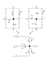
図1、図2に、本発明の第1の実施例を示す。図1、図2は、各々第1、第2の発明及びに第3、第4の発明に相当し、直流電源の電位Cmに接続される半導体素子は逆耐圧を有するIGBTで、かつモジュールの形状は図6に示す外観構造である。図5、図7は、本モジュールを3レベルインバータ(直流から交流への変換器)に適用する場合の実施例である。
図1のモジュールMJ1は、コレクタが直流電源の正極に接続されるIGBTT1と、アノードが直流電源の負極に接続されるダイオードD2と、双方向スイッチ用逆阻止型IGBTT4を内蔵し、端子PにIGBTT1のコレクタが、端子Mに逆阻止型IGBTT4のコレクタが、端子Uに逆阻止型IGBTT1のエミッタとIGBTT1のエミッタとダイオードD2との接続点が、各々接続された構成である。
1 and 2 show a first embodiment of the present invention. 1 and 2 correspond to the first and second inventions and the third and fourth inventions, respectively, and the semiconductor element connected to the potential Cm of the DC power source is an IGBT having a reverse breakdown voltage, and the module. The shape is the external structure shown in FIG. 5 and 7 show an embodiment in which this module is applied to a three-level inverter (DC to AC converter).
The module MJ1 of FIG. 1 incorporates an IGBTTT1 whose collector is connected to the positive electrode of the DC power supply, a diode D2 whose anode is connected to the negative electrode of the DC power supply, and a reverse blocking IGBTTT4 for bidirectional switch. The collector of the reverse blocking IGBTTT4 is connected to the terminal M, and the connection point of the emitter of the reverse blocking IGBTTT1, the emitter of the IGBTTT1, and the diode D2 is connected to the terminal U.
図2のモジュールMJ2は、エミッタが直流電源の負極に接続されるIGBTT2と、カソードが直流電源の正極に接続されるダイオードD1と、双方向スイッチ用逆阻止型IGBTT3を内蔵し、端子NにIGBTT2のエミッタが、端子Mに逆阻止型IGBTT3のエミッタが、端子UにIGBTT2のコレクタと逆阻止型IGBTT3のコレクタとダイオードD1のアノードとの接続点が、各々接続されたた構成である。 The module MJ2 in FIG. 2 incorporates an IGBTTT2 whose emitter is connected to the negative electrode of the DC power supply, a diode D1 whose cathode is connected to the positive electrode of the DC power supply, and a reverse blocking IGBTTT3 for bidirectional switch. The emitter of the reverse blocking IGBTTT3 is connected to the terminal M, and the connection point of the collector of the IGBTTT2, the collector of the reverse blocking IGBTTT3, and the anode of the diode D1 is connected to the terminal U.
図5に、上記モジュールMJ1とMJ2を用いて、3レベルインバータの1相分の回路を構成した回路図を示す。各モジュールの端子P同士、端子N同士、及び端子U同士を、各々接続することにより、3レベルインバータの1相分の回路を構成している。 FIG. 5 shows a circuit diagram in which a circuit for one phase of a three-level inverter is configured using the modules MJ1 and MJ2. A circuit for one phase of the three-level inverter is configured by connecting terminals P, terminals N, and terminals U of each module.
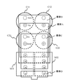
図6に、上記モジュールMJ1とMJ2の外観図を示す。また、図7にモジュールMJ1とMJ2と直流電源としてのコンデンサ直列回路に導体で配線した構造図例を示す。コンデンサC11とC12、及びコンデンサC21とC22は、各々並列接続され、さらに直列接続されて、直流電源を構成している。 FIG. 6 shows an external view of the modules MJ1 and MJ2. FIG. 7 shows an example of a structural diagram in which the modules MJ1 and MJ2 and a capacitor series circuit as a DC power source are wired with a conductor. Capacitors C11 and C12 and capacitors C21 and C22 are connected in parallel and further connected in series to constitute a DC power supply.
各モジュールの端子列が平行となるように隣接して配置し、各モジュールの端子Pと並列接続されたコンデンサC11、C12の正側電位Cpとは導体Aで、各モジュールの端子Mと並列接続されたコンデンサC11、C12の中点電位Cm1とコンデンサC21、C21の中点電位Cm2は導体Bで、各モジュールの端子Nと並列接続されたコンデンサC21、C22の負側電位Cnは導体Cで、各々接続される。
また、各モジュールの端子Uは導体Dで接続され、交流端子となる。
The positive side potential Cp of the capacitors C11 and C12 arranged adjacent to each other so that the terminal rows of the modules are parallel to each other and connected in parallel to the terminals P of the modules is a conductor A and connected in parallel to the terminals M of the modules. The midpoint potential Cm1 of the capacitors C11 and C12 and the midpoint potential Cm2 of the capacitors C21 and C21 are the conductor B, and the negative potential Cn of the capacitors C21 and C22 connected in parallel with the terminal N of each module is the conductor C. Each is connected.
Moreover, the terminal U of each module is connected by the conductor D and becomes an AC terminal.
上述のように、モジュールMJ1、MJ2を端子列が平行となるように隣接配置することで、各モジュールの端子P、M、N、U同士を近接させることが可能となる。この結果、図7に示すようにコンデンサとモジュール間の配線長を短く、かつ低配線インダクタンス化することを目的に、平行平板構造とすることが容易に実現できる。
この構成を3個用いることにより、3相3レベルインバータや3相3レベルコンバータを構成できる。
As described above, the modules PJ, M, N, and U of each module can be brought close to each other by arranging the modules MJ1 and MJ2 so that the terminal rows are parallel to each other. As a result, as shown in FIG. 7, a parallel plate structure can be easily realized for the purpose of shortening the wiring length between the capacitor and the module and reducing the wiring inductance.
By using three of these configurations, a three-phase three-level inverter or a three-phase three-level converter can be configured.
図8に、インバータ運転中の電流の転流動作モード1の例を示す。直流電源から負荷側(リアクトルLo側)へ電流を流している時の動作である。図8(a)の状態からIGBTT1がターンオフした場合、図8(b)に示すようにIGBTT4側に電流は転流する。また図8(b)の状態からIGBTT1がターンオンした場合は、図8(a)に示すようにIGBTT1側に電流は転流する。
FIG. 8 shows an example of current
一方、図8(b)の状態からIGBTT4がターンオフした場合は、図8(c)に示すようにダイオードD2側に電流は転流する。また(c)の状態からIGBTT4がターンオンした場合は、図8(b)に示すようにIGBTT4側に電流は転流する。 On the other hand, when the IGBTTT 4 is turned off from the state of FIG. 8B, the current commutates to the diode D2 side as shown in FIG. 8C. When the IGBTTT4 is turned on from the state (c), the current commutates to the IGBTTT4 side as shown in FIG. 8 (b).
図9に、インバータ運転中の電流の転流動作モード2の例を示す。負荷側(リアクトルLo側)から直流電源へ電流を流している時の動作である。図9(a)の状態からIGBTT2がターンオフした場合、図9(b)に示すようにIGBTT3側に電流は転流する。また図9(b)の状態からIGBTT2がターンオンした場合は、図9(a)に示すようにIGBTT2側に電流は転流する。 FIG. 9 shows an example of current commutation operation mode 2 during inverter operation. This is an operation when a current is flowing from the load side (reactor Lo side) to the DC power supply. When the IGBTTT2 is turned off from the state of FIG. 9A, the current commutates to the IGBTTT3 side as shown in FIG. 9B. Further, when the IGBTTT2 is turned on from the state shown in FIG. 9B, the current commutates to the IGBTTT2 side as shown in FIG. 9A.
一方、図9(b)の状態からIGBTT3がターンオフした場合は、図9(c)に示すようにダイオードD1側に電流は転流する。また図9(c)の状態からIGBTT3がターンオンした場合は、図9(b)に示すようにIGBTT3側に電流は転流する。
On the other hand, when the
以上のように、図8に示す出力電流の極性では、IGBTT1、T4、又はダイオードD2が導通するため、図1のモジュールMJ1であれば、外部配線を介さずに転流することが可能である。また、図9に示す出力電流の極性では、IGBTT2、T3又はダイオードD1が導通するため、図2のモジュールMJ2であれば、外部配線を介さずに転流することが可能である。 As described above, in the polarity of the output current shown in FIG. 8, since the IGBTTT1, T4, or the diode D2 conducts, the module MJ1 of FIG. 1 can be commutated without going through external wiring. . Further, since the IGBTTT2, T3 or the diode D1 is conducted with the polarity of the output current shown in FIG. 9, the module MJ2 in FIG. 2 can be commutated without going through the external wiring.
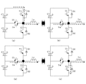
図3、図4に、本発明の第2の実施例を示す。第1の実施例との違いは、直流電源の中点電位Cm(Cm1、Cm2)に接続される双方向スイッチ用の素子として逆耐圧を有しないIGBTとダイオードとの直列回路を用いている点である。 3 and 4 show a second embodiment of the present invention. The difference from the first embodiment is that a series circuit of an IGBT and a diode having no reverse withstand voltage is used as an element for a bidirectional switch connected to the midpoint potential Cm (Cm1, Cm2) of the DC power supply. It is.
図3に示すモジュールMJ3は、実施例1におけるモジュール1の逆耐圧を有するIGBTT4の代わりに、ダイオードD4とIGBTT4aとの直列回路を、また図4に示すモジュールMJ4は、モジュール2の逆耐圧を有するIGBTT3の代わりに、ダイオードD3とIGBTT3aとの直列回路を、各々用いた構成である。ここで、ダイオードD4とIGBTT4aとの直列接続順序、及びダイオードD3とIGBTT3aとの直列接続順序は、逆でも良い。また、主回路構成及び動作は、第1の実施例と同様である。
A module MJ3 shown in FIG. 3 has a series circuit of a diode D4 and an IGBTTT4a instead of the IGBTTT4 having the reverse withstand voltage of the
尚、上記実施例には直流から交流を作り出すインバータ回路への適用例を示したが、交流から直流を作り出すコンバータ(PWM整流器)回路への適用も同様である。 In the above embodiment, an example of application to an inverter circuit that generates alternating current from direct current is shown, but the same applies to a converter (PWM rectifier) circuit that generates direct current from alternating current.
図10に、本発明の第3の実施例を示す。5レベル電力変換回路への適用例である。直流電源としてのコンデンサC1〜C4を直列接続し、最も高い電位がCp、最も低い電位がCnで、5つの電位をつくり、各電位をスイッチ回路で、リアクトルLoを介して負荷側に供給する5レベルインバータの1相分の構成である。図7に示した3レベルインバータの構成を5レベル化したもので、3レベルインバータ回路と同様に、本発明のパワー半導体モジュールを適用することができる。コンデンサの直列接続数とスイッチ回路を変更することにより、レベルを自由に変更することができる。
図10の構成では、図1に示したパワー半導体モジュールMJ1と、図2に示したパワー半導体モジュールMJ2を用いて、最も高い電位Cp、最も低い電位Cn、及び中間の電位(Cm3、Cm4)をリアクトルLoに出力し、第2番目に高い電位(Cm5、Cm6)は双方向スイッチBDS2で、第4番目に高い電位(Cm1、Cm2)は双方向スイッチBDS1で、各々リアクトルLoに出力する構成である。モジュールMJ1とMJ2を隣接して配置することにより、3レベル変換回路と同様の効果が得られる。
また、3レベルインバータやコンバータと同様に、モジュールMJ1とMJ2の代わりに、モジュールMJ3とMJ4を、各々用いることができる。
FIG. 10 shows a third embodiment of the present invention. This is an application example to a five-level power conversion circuit. Capacitors C1 to C4 as DC power supplies are connected in series, and the highest potential is Cp and the lowest potential is Cn. Five potentials are generated, and each potential is supplied to the load side via a reactor Lo by a switch circuit. It is the structure for one phase of a level inverter. The configuration of the three-level inverter shown in FIG. 7 is made into five levels, and the power semiconductor module of the present invention can be applied similarly to the three-level inverter circuit. The level can be freely changed by changing the number of capacitors connected in series and the switch circuit.
In the configuration of FIG. 10, the power semiconductor module MJ1 shown in FIG. 1 and the power semiconductor module MJ2 shown in FIG. 2 are used to obtain the highest potential Cp, the lowest potential Cn, and intermediate potentials (Cm3, Cm4). It outputs to the reactor Lo, and the second highest potential (Cm5, Cm6) is output to the reactor Lo by the bidirectional switch BDS2 and the fourth highest potential (Cm1, Cm2) is output to the reactor Lo by the bidirectional switch BDS1. is there. By arranging the modules MJ1 and MJ2 adjacent to each other, the same effect as the three-level conversion circuit can be obtained.
Similarly to the three-level inverter and converter, the modules MJ3 and MJ4 can be used instead of the modules MJ1 and MJ2.
尚、分割された直流電源と、直流電源間に接続された二つの半導体スイッチの直列回路を用い、半導体スイッチの直列接続点と直流電源の分割点との間に双方向スイッチを接続する構成であれば、コンバータ、インバータのいずれでも実現可能である。 In addition, it is a configuration in which a bidirectional switch is connected between the series connection point of the semiconductor switch and the division point of the DC power source using a divided DC power source and a series circuit of two semiconductor switches connected between the DC power sources. If so, it can be realized by either a converter or an inverter.
本発明は、3レベル以上の変換回路に適用できるパワー半導体モジュールとそれを適用した変換回路の提案であり、無停電電源装置、電動機駆動装置、系統連系装置などへの適用が可能である。 The present invention is a proposal of a power semiconductor module that can be applied to a conversion circuit of three or more levels and a conversion circuit to which the power semiconductor module is applied, and can be applied to an uninterruptible power supply device, an electric motor drive device, a grid interconnection device, and the like.
1・・・交流電源 2・・・負荷
3、5、7、8、T1、T2、T3a、T4a・・・IGBT
12、13、T3、T4・・・逆阻止型IGBT
BDS1、BDS2・・・双方向スイッチ
4、6、9、10、D1、D2、D3、D4・・・ダイオード
C1、C2、C3、C4、C11、C12、C21、C22・・・コンデンサ
Lo、Li・・・リアクトル 11・・・交流端子
CONV・・・コンバータ(PWM整流器) INV・・・インバータ
MJ0、MJ1、MJ2、MJ3、MJ4・・・半導体モジュール
導体A〜D・・・導体
DESCRIPTION OF
12, 13, T3, T4 ... reverse blocking IGBT
BDS1, BDS2 ...
Claims (10)
Priority Applications (4)
| Application Number | Priority Date | Filing Date | Title |
|---|---|---|---|
| JP2010087471A JP5494147B2 (en) | 2010-04-06 | 2010-04-06 | Power semiconductor module and power converter using the same |
| CN201110051644.XA CN102214644B (en) | 2010-04-06 | 2011-02-22 | Power semiconductor device and power conversion system using the device |
| DE201110005184 DE102011005184A1 (en) | 2010-04-06 | 2011-03-07 | Power semiconductor device and this power conversion system using |
| US13/042,999 US8901602B2 (en) | 2010-04-06 | 2011-03-08 | Power semiconductor device and power conversion system using the device |
Applications Claiming Priority (1)
| Application Number | Priority Date | Filing Date | Title |
|---|---|---|---|
| JP2010087471A JP5494147B2 (en) | 2010-04-06 | 2010-04-06 | Power semiconductor module and power converter using the same |
Publications (3)
| Publication Number | Publication Date |
|---|---|
| JP2011223666A JP2011223666A (en) | 2011-11-04 |
| JP2011223666A5 JP2011223666A5 (en) | 2013-05-16 |
| JP5494147B2 true JP5494147B2 (en) | 2014-05-14 |
Family
ID=44709495
Family Applications (1)
| Application Number | Title | Priority Date | Filing Date |
|---|---|---|---|
| JP2010087471A Active JP5494147B2 (en) | 2010-04-06 | 2010-04-06 | Power semiconductor module and power converter using the same |
Country Status (4)
| Country | Link |
|---|---|
| US (1) | US8901602B2 (en) |
| JP (1) | JP5494147B2 (en) |
| CN (1) | CN102214644B (en) |
| DE (1) | DE102011005184A1 (en) |
Families Citing this family (14)
| Publication number | Priority date | Publication date | Assignee | Title |
|---|---|---|---|---|
| JP5493532B2 (en) * | 2009-07-17 | 2014-05-14 | 富士電機株式会社 | Load driving device and electric vehicle using the same |
| JP5724314B2 (en) * | 2010-11-16 | 2015-05-27 | 富士電機株式会社 | Power semiconductor module |
| US20140362626A1 (en) * | 2011-12-28 | 2014-12-11 | Panasonic Corporation | Multilevel inverter device |
| JP5891940B2 (en) * | 2012-05-17 | 2016-03-23 | 富士電機株式会社 | 3-level unit inverter |
| CN103904928A (en) * | 2014-04-23 | 2014-07-02 | 西华大学 | Serial-parallel mixing type three-level NPP inversion topological unit and three-level inverter |
| CN105226975B (en) * | 2014-06-06 | 2017-12-15 | 台达电子企业管理(上海)有限公司 | TNPC DC-to-AC converters and its bridgc arm short detection method |
| WO2016031295A1 (en) * | 2014-08-26 | 2016-03-03 | 富士電機株式会社 | Three-level power conversion device |
| JP6304017B2 (en) * | 2014-12-18 | 2018-04-04 | 三菱電機株式会社 | Semiconductor device |
| WO2018056213A1 (en) | 2016-09-23 | 2018-03-29 | 三菱電機株式会社 | Power semiconductor module and power semiconductor device |
| JP6702429B2 (en) * | 2016-11-16 | 2020-06-03 | 富士電機株式会社 | Semiconductor test circuit, semiconductor test apparatus, and semiconductor test method |
| JP2018107857A (en) * | 2016-12-22 | 2018-07-05 | 富士電機株式会社 | Power conversion apparatus |
| JP2019180114A (en) * | 2018-03-30 | 2019-10-17 | 本田技研工業株式会社 | Power conversion device and capacitor for power conversion device |
| CN108551159B (en) * | 2018-04-08 | 2019-06-11 | 科华恒盛股份有限公司 | Reverse blocking IGBT short-circuit protection circuit, method and system and storage medium |
| JP7039430B2 (en) * | 2018-09-19 | 2022-03-22 | 株式会社東芝 | AC / DC converter |
Family Cites Families (15)
| Publication number | Priority date | Publication date | Assignee | Title |
|---|---|---|---|---|
| JP3263317B2 (en) | 1996-06-18 | 2002-03-04 | 株式会社東芝 | Switching module and power converter using the module |
| CN1242604A (en) * | 1998-06-26 | 2000-01-26 | 株式会社东芝 | Semiconductor protective device and power conversion device |
| JP2000216331A (en) | 1999-01-25 | 2000-08-04 | Mitsubishi Electric Corp | Power semiconductor module and electric conversion device using the module |
| WO2001031771A1 (en) * | 1999-10-27 | 2001-05-03 | Hitachi, Ltd. | Electric power converter |
| JP2002026251A (en) | 2000-07-11 | 2002-01-25 | Toshiba Corp | Semiconductor device |
| JP2002231883A (en) | 2001-01-31 | 2002-08-16 | Hitachi Ltd | Power semiconductor module and power conversion device using the same |
| JP2003018854A (en) | 2001-07-02 | 2003-01-17 | Honda Motor Co Ltd | Resonance-type inverter device |
| US6838925B1 (en) * | 2003-10-07 | 2005-01-04 | American Power Conversion Corporation | Three level inverter |
| US7289329B2 (en) * | 2004-06-04 | 2007-10-30 | Siemens Vdo Automotive Corporation | Integration of planar transformer and/or planar inductor with power switches in power converter |
| JP4728718B2 (en) * | 2005-07-15 | 2011-07-20 | ローム株式会社 | STEP-UP SWITCHING REGULATOR, ITS CONTROL CIRCUIT, AND ELECTRONIC DEVICE USING THE SAME |
| JP2008193779A (en) * | 2007-02-02 | 2008-08-21 | Fuji Electric Systems Co Ltd | Semiconductor module |
| JP2009022062A (en) * | 2007-07-10 | 2009-01-29 | Fuji Electric Systems Co Ltd | Wiring structure of 3-level power conversion circuit |
| JP5440335B2 (en) * | 2010-04-06 | 2014-03-12 | 富士電機株式会社 | Power semiconductor module and power converter using the same |
| JP2012029429A (en) * | 2010-07-22 | 2012-02-09 | Fuji Electric Co Ltd | Three level power conversion device |
| JP5724314B2 (en) * | 2010-11-16 | 2015-05-27 | 富士電機株式会社 | Power semiconductor module |
-
2010
- 2010-04-06 JP JP2010087471A patent/JP5494147B2/en active Active
-
2011
- 2011-02-22 CN CN201110051644.XA patent/CN102214644B/en active Active
- 2011-03-07 DE DE201110005184 patent/DE102011005184A1/en active Pending
- 2011-03-08 US US13/042,999 patent/US8901602B2/en active Active
Also Published As
| Publication number | Publication date |
|---|---|
| US8901602B2 (en) | 2014-12-02 |
| US20110242860A1 (en) | 2011-10-06 |
| JP2011223666A (en) | 2011-11-04 |
| DE102011005184A1 (en) | 2011-11-03 |
| CN102214644B (en) | 2015-02-25 |
| CN102214644A (en) | 2011-10-12 |
Similar Documents
| Publication | Publication Date | Title |
|---|---|---|
| JP5494147B2 (en) | Power semiconductor module and power converter using the same | |
| JP5440335B2 (en) | Power semiconductor module and power converter using the same | |
| JP5369922B2 (en) | 3-level power converter | |
| JP5450635B2 (en) | Power converter | |
| JP5457449B2 (en) | Power converter | |
| JP5515386B2 (en) | Snubber circuit for three-level power converter | |
| US20150155770A1 (en) | Five-level rectifier | |
| US10003280B2 (en) | Semiconductor module, upper and lower arm kit, and three-level inverter | |
| US20130088901A1 (en) | Multilevel inverter | |
| JP2008193779A (en) | Semiconductor module | |
| CN103797702A (en) | Multilevel power conversion circuit | |
| JP2015035902A (en) | Multi-level power converting device | |
| JP2009022062A (en) | Wiring structure of 3-level power conversion circuit | |
| JP2011254672A (en) | Power semiconductor module and power conversion device using the same | |
| JP5446541B2 (en) | Power converter | |
| JP2015027170A (en) | Dc/ac conversion device | |
| KR20140110037A (en) | Power conversion device | |
| JP5780907B2 (en) | Power converter | |
| JP7446932B2 (en) | Power conversion equipment and switching equipment | |
| JP2011234544A (en) | Power semiconductor module and power conversion equipment using it | |
| JPWO2018127945A1 (en) | Power converter | |
| JP5488244B2 (en) | Power semiconductor module | |
| JP6175946B2 (en) | Resonant inverter device | |
| JP5423264B2 (en) | Power converter | |
| JP2009005447A (en) | Power converter circuit |
Legal Events
| Date | Code | Title | Description |
|---|---|---|---|
| A521 | Request for written amendment filed |
Free format text: JAPANESE INTERMEDIATE CODE: A523 Effective date: 20130401 |
|
| A621 | Written request for application examination |
Free format text: JAPANESE INTERMEDIATE CODE: A621 Effective date: 20130401 |
|
| A977 | Report on retrieval |
Free format text: JAPANESE INTERMEDIATE CODE: A971007 Effective date: 20131212 |
|
| TRDD | Decision of grant or rejection written | ||
| A01 | Written decision to grant a patent or to grant a registration (utility model) |
Free format text: JAPANESE INTERMEDIATE CODE: A01 Effective date: 20140204 |
|
| A61 | First payment of annual fees (during grant procedure) |
Free format text: JAPANESE INTERMEDIATE CODE: A61 Effective date: 20140217 |
|
| R150 | Certificate of patent or registration of utility model |
Ref document number: 5494147 Country of ref document: JP Free format text: JAPANESE INTERMEDIATE CODE: R150 |
|
| R250 | Receipt of annual fees |
Free format text: JAPANESE INTERMEDIATE CODE: R250 |
|
| R250 | Receipt of annual fees |
Free format text: JAPANESE INTERMEDIATE CODE: R250 |
|
| R250 | Receipt of annual fees |
Free format text: JAPANESE INTERMEDIATE CODE: R250 |
|
| R250 | Receipt of annual fees |
Free format text: JAPANESE INTERMEDIATE CODE: R250 |
|
| R250 | Receipt of annual fees |
Free format text: JAPANESE INTERMEDIATE CODE: R250 |
|
| R250 | Receipt of annual fees |
Free format text: JAPANESE INTERMEDIATE CODE: R250 |
|
| R250 | Receipt of annual fees |
Free format text: JAPANESE INTERMEDIATE CODE: R250 |
|
| R250 | Receipt of annual fees |
Free format text: JAPANESE INTERMEDIATE CODE: R250 |