EP1168006A2 - Verfahren zum Verbinden einer Vielzahl von optischen Elementen mit einem Grundkörper - Google Patents
Verfahren zum Verbinden einer Vielzahl von optischen Elementen mit einem Grundkörper Download PDFInfo
- Publication number
- EP1168006A2 EP1168006A2 EP01112204A EP01112204A EP1168006A2 EP 1168006 A2 EP1168006 A2 EP 1168006A2 EP 01112204 A EP01112204 A EP 01112204A EP 01112204 A EP01112204 A EP 01112204A EP 1168006 A2 EP1168006 A2 EP 1168006A2
- Authority
- EP
- European Patent Office
- Prior art keywords
- base body
- mirror
- optical elements
- elements
- supporting structure
- Prior art date
- Legal status (The legal status is an assumption and is not a legal conclusion. Google has not performed a legal analysis and makes no representation as to the accuracy of the status listed.)
- Granted
Links
Images

Classifications
-
- G—PHYSICS
- G03—PHOTOGRAPHY; CINEMATOGRAPHY; ANALOGOUS TECHNIQUES USING WAVES OTHER THAN OPTICAL WAVES; ELECTROGRAPHY; HOLOGRAPHY
- G03F—PHOTOMECHANICAL PRODUCTION OF TEXTURED OR PATTERNED SURFACES, e.g. FOR PRINTING, FOR PROCESSING OF SEMICONDUCTOR DEVICES; MATERIALS THEREFOR; ORIGINALS THEREFOR; APPARATUS SPECIALLY ADAPTED THEREFOR
- G03F7/00—Photomechanical, e.g. photolithographic, production of textured or patterned surfaces, e.g. printing surfaces; Materials therefor, e.g. comprising photoresists; Apparatus specially adapted therefor
- G03F7/70—Microphotolithographic exposure; Apparatus therefor
- G03F7/708—Construction of apparatus, e.g. environment aspects, hygiene aspects or materials
- G03F7/70808—Construction details, e.g. housing, load-lock, seals or windows for passing light in or out of apparatus
- G03F7/70825—Mounting of individual elements, e.g. mounts, holders or supports
-
- B—PERFORMING OPERATIONS; TRANSPORTING
- B23—MACHINE TOOLS; METAL-WORKING NOT OTHERWISE PROVIDED FOR
- B23K—SOLDERING OR UNSOLDERING; WELDING; CLADDING OR PLATING BY SOLDERING OR WELDING; CUTTING BY APPLYING HEAT LOCALLY, e.g. FLAME CUTTING; WORKING BY LASER BEAM
- B23K26/00—Working by laser beam, e.g. welding, cutting or boring
- B23K26/02—Positioning or observing the workpiece, e.g. with respect to the point of impact; Aligning, aiming or focusing the laser beam
- B23K26/06—Shaping the laser beam, e.g. by masks or multi-focusing
- B23K26/064—Shaping the laser beam, e.g. by masks or multi-focusing by means of optical elements, e.g. lenses, mirrors or prisms
- B23K26/0643—Shaping the laser beam, e.g. by masks or multi-focusing by means of optical elements, e.g. lenses, mirrors or prisms comprising mirrors
-
- B—PERFORMING OPERATIONS; TRANSPORTING
- B23—MACHINE TOOLS; METAL-WORKING NOT OTHERWISE PROVIDED FOR
- B23K—SOLDERING OR UNSOLDERING; WELDING; CLADDING OR PLATING BY SOLDERING OR WELDING; CUTTING BY APPLYING HEAT LOCALLY, e.g. FLAME CUTTING; WORKING BY LASER BEAM
- B23K28/00—Welding or cutting not covered by groups B23K5/00 - B23K26/00
- B23K28/006—Welding metals by means of an electrolyte
-
- C—CHEMISTRY; METALLURGY
- C25—ELECTROLYTIC OR ELECTROPHORETIC PROCESSES; APPARATUS THEREFOR
- C25D—PROCESSES FOR THE ELECTROLYTIC OR ELECTROPHORETIC PRODUCTION OF COATINGS; ELECTROFORMING; APPARATUS THEREFOR
- C25D1/00—Electroforming
-
- C—CHEMISTRY; METALLURGY
- C25—ELECTROLYTIC OR ELECTROPHORETIC PROCESSES; APPARATUS THEREFOR
- C25D—PROCESSES FOR THE ELECTROLYTIC OR ELECTROPHORETIC PRODUCTION OF COATINGS; ELECTROFORMING; APPARATUS THEREFOR
- C25D5/00—Electroplating characterised by the process; Pretreatment or after-treatment of workpieces
- C25D5/02—Electroplating of selected surface areas
- C25D5/022—Electroplating of selected surface areas using masking means
-
- G—PHYSICS
- G02—OPTICS
- G02B—OPTICAL ELEMENTS, SYSTEMS OR APPARATUS
- G02B5/00—Optical elements other than lenses
- G02B5/08—Mirrors
- G02B5/09—Multifaceted or polygonal mirrors, e.g. polygonal scanning mirrors; Fresnel mirrors
-
- G—PHYSICS
- G03—PHOTOGRAPHY; CINEMATOGRAPHY; ANALOGOUS TECHNIQUES USING WAVES OTHER THAN OPTICAL WAVES; ELECTROGRAPHY; HOLOGRAPHY
- G03F—PHOTOMECHANICAL PRODUCTION OF TEXTURED OR PATTERNED SURFACES, e.g. FOR PRINTING, FOR PROCESSING OF SEMICONDUCTOR DEVICES; MATERIALS THEREFOR; ORIGINALS THEREFOR; APPARATUS SPECIALLY ADAPTED THEREFOR
- G03F7/00—Photomechanical, e.g. photolithographic, production of textured or patterned surfaces, e.g. printing surfaces; Materials therefor, e.g. comprising photoresists; Apparatus specially adapted therefor
- G03F7/70—Microphotolithographic exposure; Apparatus therefor
- G03F7/70058—Mask illumination systems
- G03F7/702—Reflective illumination, i.e. reflective optical elements other than folding mirrors, e.g. extreme ultraviolet [EUV] illumination systems
-
- Y—GENERAL TAGGING OF NEW TECHNOLOGICAL DEVELOPMENTS; GENERAL TAGGING OF CROSS-SECTIONAL TECHNOLOGIES SPANNING OVER SEVERAL SECTIONS OF THE IPC; TECHNICAL SUBJECTS COVERED BY FORMER USPC CROSS-REFERENCE ART COLLECTIONS [XRACs] AND DIGESTS
- Y10—TECHNICAL SUBJECTS COVERED BY FORMER USPC
- Y10S—TECHNICAL SUBJECTS COVERED BY FORMER USPC CROSS-REFERENCE ART COLLECTIONS [XRACs] AND DIGESTS
- Y10S359/00—Optical: systems and elements
- Y10S359/90—Methods
Definitions
- the invention relates to a method for connecting a plurality of optical elements with a base body, in particular for making a faceted mirror.
- the invention relates also a facet mirror produced by the process.
- a method is known from US Pat. No. 4,277,141, according to which a Multifaceted mirror is manufactured in several steps, namely, in a first step, individual mirrors are created, the individual mirrors are then fixed and aligned and connected to a support body via an adhesive.
- a facet mirror is described in US Pat. No. 4,195,913 a large number of individual mirrors on a spherical support structure is glued or screwed on.
- the object of the present invention is a method for connecting a variety of optical elements of the to create the type mentioned, the variety of optical Elements with high accuracy, especially with regard to Position and angularity on which the base body is arranged can so that e.g. Jet mixtures and field images with high precision can be done.
- the present invention is also based on the object a faceted mirror with a variety of individual optical To form mirror elements of a homogeneous lighting distribution or homogeneous illumination and a very exact Beam mixing and field mapping generated.
- the object is characterized by Part of claim 1 mentioned method solved.
- the method according to the invention allows a large number of individual optical elements that are completely identical can be done in a relatively simple way and very precisely the galvanizing process with each other and with a basic body get connected. Because exactly through the electroplating process understandable relationships can be created this way e.g. form a faceted mirror that reflects the homogeneous Illumination of a field enables, with which a corresponding good beam mixing and exact field mapping are possible.
- a jet mixture can be mixed with the method according to the invention or achieve lighting that is disadvantageous higher light intensity in the middle area eliminated. This is especially in optical lithography with an EUV lighting system advantageous, e.g. on the reticle (Mask) have the largest possible homogeneously illuminated area would like to.
- the process according to the invention practically turns it into a monolithic one Body formed by good heat transfer of the individual optical elements to the basic body an efficient Allows cooling of the optical element.
- the following is a method for making a faceted mirror and a facet mirror made by the method described for example.
- the procedure is basically but also for connecting or assembling other optical Elements such as Lenses and lens arrays, suitable.
- In 1 shows the use of a facet mirror 1 in one Illumination system shown for EUV lithography.
- the light from a source 2, e.g. of a laser, is over a Collector mirror 3 thrown on the facet mirror 1 where it is with the desired uniform illumination via a deflecting mirror 4 a reticle (mask) 5 is supplied.
- the pattern of the reticle 5 is a not shown
- Projection lens 6 a wafer 7 for imaging the image fed from reticle 5.
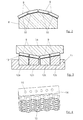
- the production of the faceted mirror 1 with a correspondingly high level Precision and homogeneous or desired illumination takes place 2 on a base body 8.
- the base body 8 can e.g. be galvanically molded, with its functional surface in terms of curvature, position and location of the requirements corresponds to that are placed on the finished facet mirror 1. Only the surface quality is still missing. The surface quality is now by individual mirror elements 9 as optical Elements realized.
- the Making a faceted mirror also easier, simplified and inexpensive.
- Bad qualities of mirror elements can be discarded beforehand or one can make a selection of mirror elements 9 that are identical or are almost identical, especially with regard to their optical Characteristics.
- Galvanizing processes are well known, which is why here is not discussed in more detail. Basically, this is done in that the mirror elements 9 on the base body 8 in their position will be brought and the whole then in an electrolytic Bad is switched cathodically and as the anode desired material, e.g. Cu or Ni is used so that the parts can grow together into one unit. To this Way you can e.g. the growth of a copper layer with any Reach thickness.
- anode desired material e.g. Cu or Ni
- the mirror elements 9 placed on the base body 8 become connected to the base body 8 by a galvanoplastic joining, like this through an intermediate layer 10 between mirror elements 9 and the base body 8 is indicated.
- an auxiliary structure 11 can be used according to FIG Positioning of the mirror elements 9 can be provided.
- the Auxiliary structure can consist of several individual stamps for more precise adjustment 12a, 12b, 12c ... be put together, that together a surface in negative form for the facet mirror to be produced form and correspondingly with a spherical surface are at a distance from each other or gaps for reasons of space provide.
- the mirror elements are e.g. through an adhesive or a Resin 13, with its mirrored side on the auxiliary structure 11 fixed.
- an adhesive or a Resin 13 With its mirrored side on the auxiliary structure 11 fixed.
- lens arrays When lens arrays are formed, the individual also become Lenses each with one of the optical surfaces on the Auxiliary structure 11 fixed.
- the second optical surfaces must then be protected separately from contamination. lenses or non-conductive mirror elements must first be replaced by a appropriate coating can be made electrically conductive.
- FIG. 14 After completion of a sufficiently strong supporting structure 14, can subsequently or in parallel with growing up Stiffening structures are installed by galvanic means or you let them grow up accordingly.
- 4 is a honeycomb structure 15 (without Mirror elements) shown.
- FIG can be seen that the support structure 14 with a cooling system in Form of cooling channels 16 may be provided.
- the cooling channels 16 can during the electroplating process be molded. All that is required is that corresponding snake-shaped wax inserts are provided, which then be melted out.
- Another solution can be to use a copper pipe hangs in a snake shape and this then during the galvanizing process ingrows. This way you get one very good heat transfer due to a metallic connection.
Landscapes
- Physics & Mathematics (AREA)
- Engineering & Computer Science (AREA)
- Chemical & Material Sciences (AREA)
- General Physics & Mathematics (AREA)
- Optics & Photonics (AREA)
- Chemical Kinetics & Catalysis (AREA)
- Electrochemistry (AREA)
- Materials Engineering (AREA)
- Metallurgy (AREA)
- Organic Chemistry (AREA)
- Mechanical Engineering (AREA)
- Health & Medical Sciences (AREA)
- Environmental & Geological Engineering (AREA)
- Epidemiology (AREA)
- Public Health (AREA)
- Plasma & Fusion (AREA)
- Exposure And Positioning Against Photoresist Photosensitive Materials (AREA)
- Optical Elements Other Than Lenses (AREA)
- Exposure Of Semiconductors, Excluding Electron Or Ion Beam Exposure (AREA)
- Mounting And Adjusting Of Optical Elements (AREA)
- Microscoopes, Condenser (AREA)
- Laser Beam Processing (AREA)
Abstract
Description
- Figur 1
- Prinzipdarstellung eines in einem EUV-Beleuchtungssystem für die Mikrolithographie angeordneten erfindungsgemäßen Facettenspiegels,
- Figur 2
- ein erstes Herstellungsverfahren für einen Facettenspiegel,
- Figur 3
- ein zweites Herstellungsverfahren für einen Facettenspiegel, und
- Figur 4
- einen Grundkörper für einen Facettenspiegel mit Versteifungen in Wabenstruktur und mit Kühlkanälen.
Claims (17)
- Verfahren zum Zusammenfügen einer Vielzahl von optischen Elementen (9) auf einem Grundkörper (8), insbesondere zum Herstellen eines Facettenspiegels, z.B. zur Strahlmischung und Feldabbildung für ein EUV-Beleuchtungssystem, wobei die einzelnen optischen Elemente (9) auf dem Grundkörper (8) positioniert und anschließend durch galvanoplastisches Fügen mit dem Grundkörper (8) verbunden werden.
- Verfahren nach Anspruch 1, dadurch gekennzeichnet, daß der Grundkörper (8) galvanisch abgeformt wird.
- Verfahren zum Verbinden einer Vielzahl von optischen Elementen mit einem Grundkörper, insbesondere zum Herstellen eines Facettenspiegels, z.B. zur Strahlmischung und Feldabbildung für ein EUV-Beleuchtungssystem, wobei die Vielzahl der optischen Elemente auf einer Hilfsstruktur (11) ausgerichtet wird und wobei man anschließend die optischen Elemente (9) auf ihren Rückseiten unter Bildung einer Tragstruktur (14) als Grundkörper galvanoplastisch zusammenwachsen läßt.
- Verfahren nach Anspruch 3, dadurch gekennzeichnet, daß der aufgewachsene Grundkörper (Tragstruktur 14) mit Versteifungen versehen ist.
- Verfahren nach Anspruch 4, dadurch gekennzeichnet, daß die Versteifungen (15) auf galvanischem Wege integriert werden.
- Verfahren nach Anspruch 5, dadurch gekennzeichnet, daß zur Versteifung der aufgewachsenen Körper (Tragstruktur 14) als Wabenstruktur (15) ausgeführt wird.
- Verfahren nach einem der Ansprüche 3 bis 6, dadurch gekennzeichnet, daß der aufgewachsene Grundkörper (Tragstruktur 14) mit Kühlkanälen (16) versehen wird.
- Verfahren nach Anspruch 7, dadurch gekennzeichnet, daß die Kühlkanäle (16) beim Galvanisierungsprozeß durch Kerne mit eingeformt werden, welche anschließend entfernt werden.
- Verfahren nach Anspruch 7, dadurch gekennzeichnet, daß die Kühlkanäle (16) durch eingelegte Rohre gebildet werden, die bei dem Galvanisierungsprozeß einwachsen.
- Verfahren nach Anspruch 3, dadurch gekennzeichnet, daß die Hilfsstruktur (11) aus mehreren Teilen (Stempel 12a, 12b,..) mit dazwischen liegenden Abstands- oder Positionshaltern gebildet wird.
- Facettenspiegel zur Strahlmischung und Feldabbildung für ein Beleuchtungssystem, wobei eine Vielzahl von Spiegelelementen auf einem Grundkörper angeordnet sind, dadurch gekennzeichnet, daß die Spiegelelemente (9) durch galvanisches Fügen mit dem Grundkörper (8,14) verbunden sind.
- Facettenspiegel nach Anspruch 11, dadurch gekennzeichnet, daß der Grundkörper (8) galvanisch abgeformt ist.
- Facettenspiegel nach Anspruch 1, dadurch gekennzeichnet, daß die Spiegelelemente (9) auf ihren Rückseiten mit einer Tragstruktur (14) als Grundkörper versehen sind, mit dem sie galvanoplastisch aufgewachsen sind.
- Facettenspiegel nach Anspruch 13, dadurch gekennzeichnet, daß der aufgewachsene Körper (Tragstruktur 14) mit Versteifungen versehen ist.
- Facettenspiegel nach Anspruch 14, dadurch gekennzeichnet, daß die Versteifungen auf galvanischem Wege hergestellt sind.
- Facettenspiegel nach Anspruch 15, dadurch gekennzeichnet, daß die Versteifungen als Wabenstruktur (15) ausgeführt sind.
- Facettenspiegel nach einem der Ansprüche 13 bis 16, dadurch gekennzeichnet, daß der aufgewachsene Körper (Tragstruktur 14) mit Kühlkanälen (16) versehen ist.
Applications Claiming Priority (2)
| Application Number | Priority Date | Filing Date | Title |
|---|---|---|---|
| DE10030495 | 2000-06-21 | ||
| DE10030495A DE10030495A1 (de) | 2000-06-21 | 2000-06-21 | Verfahren zum Verbinden einer Vielzahl von optischen Elementen mit einem Grundkörper |
Publications (3)
| Publication Number | Publication Date |
|---|---|
| EP1168006A2 true EP1168006A2 (de) | 2002-01-02 |
| EP1168006A3 EP1168006A3 (de) | 2004-03-10 |
| EP1168006B1 EP1168006B1 (de) | 2006-07-05 |
Family
ID=7646455
Family Applications (1)
| Application Number | Title | Priority Date | Filing Date |
|---|---|---|---|
| EP01112204A Expired - Lifetime EP1168006B1 (de) | 2000-06-21 | 2001-05-18 | Verfahren zum Verbinden einer Vielzahl von optischen Elementen mit einem Grundkörper |
Country Status (4)
| Country | Link |
|---|---|
| US (1) | US7034998B2 (de) |
| EP (1) | EP1168006B1 (de) |
| JP (1) | JP2002071922A (de) |
| DE (2) | DE10030495A1 (de) |
Cited By (1)
| Publication number | Priority date | Publication date | Assignee | Title |
|---|---|---|---|---|
| CN107976793A (zh) * | 2017-12-13 | 2018-05-01 | 东方宏海新能源科技发展有限公司 | 聚光镜片的制作工艺 |
Families Citing this family (10)
| Publication number | Priority date | Publication date | Assignee | Title |
|---|---|---|---|---|
| DE10030495A1 (de) | 2000-06-21 | 2002-01-03 | Zeiss Carl | Verfahren zum Verbinden einer Vielzahl von optischen Elementen mit einem Grundkörper |
| US7246909B2 (en) | 2003-01-24 | 2007-07-24 | Carl Zeiss Smt Ag | Method for the production of a facetted mirror |
| DE10302664A1 (de) * | 2003-01-24 | 2004-07-29 | Carl Zeiss Smt Ag | Verfahren zur Herstellung eines Facettenspiegels |
| DE10317667A1 (de) * | 2003-04-17 | 2004-11-18 | Carl Zeiss Smt Ag | Optisches Element für ein Beleuchtungssystem |
| WO2005006081A1 (en) * | 2003-07-09 | 2005-01-20 | Carl-Zeiss Smt Ag | Facet mirrors and a method for producing mirror facets |
| DE102005057325A1 (de) * | 2005-12-01 | 2007-06-06 | Carl Zeiss Smt Ag | Vorrichtung zur Variation der Abbildungseigenschaften eines Spiegels |
| DE102006031654A1 (de) * | 2006-04-24 | 2007-10-25 | Carl Zeiss Smt Ag | Facettenspiegel mit einer Vielzahl von Spiegelsegmenten |
| US8441747B2 (en) | 2006-09-14 | 2013-05-14 | Carl Zeiss Smt Gmbh | Optical module with minimized overrun of the optical element |
| DE102007008448A1 (de) * | 2007-02-19 | 2008-08-21 | Carl Zeiss Smt Ag | Verfahren zur Herstellung von Spiegelfacetten für einen Facettenspiegel |
| DE102021208879A1 (de) * | 2021-08-13 | 2023-02-16 | Carl Zeiss Smt Gmbh | Optisches element, projektionsoptik und projektionsbelichtungsanlage |
Family Cites Families (55)
| Publication number | Priority date | Publication date | Assignee | Title |
|---|---|---|---|---|
| DE1146667B (de) * | 1957-07-02 | 1963-04-04 | Hensoldt & Soehne M | Polygonspiegel |
| CH371906A (de) | 1958-08-11 | 1963-09-15 | Optische Ind De Oude Delft Nv | Halterung für optische Elemente |
| US3378469A (en) * | 1964-04-03 | 1968-04-16 | Electro Optical Systems Inc | Electroforming technique and structure for reflecting mirrors |
| US3837125A (en) * | 1973-09-04 | 1974-09-24 | Celestron Pacific | Method and system for making schmidt corrector lenses |
| US3917385A (en) * | 1973-09-19 | 1975-11-04 | Rockwell International Corp | Simplified micropositioner |
| FI52440C (fi) | 1975-09-04 | 1977-09-12 | Pekema Oy | Menetelmä ja laite sulan termoplastisen päällystysaineen pursottamisek si perusaineradalle siten, että päällysteaine on tietyiltä kohdin irti perusaineesta. |
| US4038971A (en) * | 1975-10-22 | 1977-08-02 | Bezborodko Joseph A I B | Concave, mirrored solar collector |
| DE2637735C3 (de) * | 1976-08-21 | 1979-12-13 | Hughes Aircraft Co., Culver City, Calif. (V.St.A.) | Vorrichtung zum Abtasten eines Blickfeldes |
| DD128439A1 (de) * | 1976-10-13 | 1977-11-16 | Wolfgang Schaefer | Verfahren zur herstellung optischer bauelemente aus kunststoffen |
| GB2010523A (en) * | 1977-10-12 | 1979-06-27 | Crosfield Electronics Ltd | Production of Reflective Surfaces |
| US4195913A (en) * | 1977-11-09 | 1980-04-01 | Spawr Optical Research, Inc. | Optical integration with screw supports |
| US4236296A (en) * | 1978-10-13 | 1980-12-02 | Exxon Research & Engineering Co. | Etch method of cleaving semiconductor diode laser wafers |
| US4338165A (en) * | 1978-11-13 | 1982-07-06 | National Association Of Theatre Owners, Inc. | Method of making a high-gain projection screen |
| US4277141A (en) * | 1979-03-28 | 1981-07-07 | Tropel, Inc. | Multifaceted mirror and assembly fixture and method of making such mirror |
| DE3030549C2 (de) * | 1980-08-13 | 1983-01-20 | Fa. Carl Zeiss, 7920 Heidenheim | Vorrichtung zur Verstellung zweier spielfrei im Gewindeeingriff befindlicher Teile |
| JPS5790607A (en) | 1980-11-28 | 1982-06-05 | Fujitsu Ltd | Optical glass fitting device |
| US4389115A (en) | 1981-08-06 | 1983-06-21 | Richter Thomas A | Optical system |
| DD204320A1 (de) * | 1981-10-30 | 1983-11-23 | Volker Eberhardt | Anordnung optischer bauelemente in mechanischen fuehrungen |
| DD215407A1 (de) | 1983-04-04 | 1984-11-07 | Zeiss Jena Veb Carl | Ringfoermige linsenfassung fuer optische systeme hoher leistung |
| FR2552554A1 (fr) * | 1983-09-23 | 1985-03-29 | Leteurtre Jean | Miroir pour faisceau lumineux, notamment laser de puissance |
| DE3544429A1 (de) | 1985-12-16 | 1987-06-19 | Juwedor Gmbh | Verfahren zur galvanoplastischen herstellung von schmuckwaren |
| US4733945A (en) | 1986-01-15 | 1988-03-29 | The Perkin-Elmer Corporation | Precision lens mounting |
| US4740276A (en) * | 1987-05-08 | 1988-04-26 | The United States Of America As Represented By The Secretary Of The Air Force | Fabrication of cooled faceplate segmented aperture mirrors (SAM) by electroforming |
| US5428482A (en) | 1991-11-04 | 1995-06-27 | General Signal Corporation | Decoupled mount for optical element and stacked annuli assembly |
| DE4136580A1 (de) | 1991-11-07 | 1993-05-13 | Zeiss Carl Fa | Objektivverstelleinrichtung und schraubengetriebe |
| DE4237775C1 (de) | 1992-11-09 | 1994-01-20 | Rodenstock Optik G | Optisches System mit einem Linsensystem und einer Lichtquelle |
| FR2706630B1 (fr) * | 1993-05-10 | 1995-09-08 | Aerospatiale | Procédé de fabrication d'un réflecteur à support en composite à matrice métallique, et réflecteur ainsi obtenu. |
| US5537262A (en) * | 1993-10-19 | 1996-07-16 | Asahi Kogaku Kogyo Kabushiki Kaisha | Rotational torque setting apparatus for screw mechanism |
| US5482482A (en) * | 1994-06-21 | 1996-01-09 | Davis; Grover W. | Air encircling marine propeller apparatus |
| DE19537137A1 (de) | 1995-10-05 | 1997-04-10 | Zeiss Carl Fa | Metallmatrix-Hohlkugel-Kompositwerkstoff |
| DE19649993A1 (de) * | 1996-11-22 | 1998-05-28 | Berliner Inst Fuer Optik Gmbh | Verfahren zur Herstellung eines ultraleichten Präzisions-Polygonspiegels mit hohem Reflexionsvermögen und danach hergestellter Polygonspiegel |
| US5891317A (en) * | 1997-02-04 | 1999-04-06 | Avon Products, Inc. | Electroformed hollow jewelry |
| DE19735831A1 (de) | 1997-08-18 | 1999-02-25 | Zeiss Carl Fa | Galvanoplastische Optik-Fassung |
| DE19807120A1 (de) * | 1998-02-20 | 1999-08-26 | Zeiss Carl Fa | Optisches System mit Polarisationskompensator |
| DE19825716A1 (de) | 1998-06-09 | 1999-12-16 | Zeiss Carl Fa | Baugruppe aus optischem Element und Fassung |
| US6118577A (en) * | 1998-08-06 | 2000-09-12 | Euv, L.L.C | Diffractive element in extreme-UV lithography condenser |
| DE19859634A1 (de) * | 1998-12-23 | 2000-06-29 | Zeiss Carl Fa | Optisches System, insbesondere Projektionsbelichtungsanlage der Mikrolithographie |
| US6373552B1 (en) * | 1999-01-20 | 2002-04-16 | Asm Lithography B.V. | Optical correction plate, and its application in a lithographic projection apparatus |
| DE19908554A1 (de) | 1999-02-27 | 2000-08-31 | Zeiss Carl Fa | Verstellbare Baugruppe |
| DE19910947A1 (de) * | 1999-03-12 | 2000-09-14 | Zeiss Carl Fa | Vorrichtung zum Verschieben eines optischen Elementes entlang der optischen Achse |
| DE19930643C2 (de) * | 1999-07-02 | 2002-01-24 | Zeiss Carl | Baugruppe aus einem optischen Element und einer Fassung |
| US6155868A (en) * | 1999-08-24 | 2000-12-05 | Hon Hai Precision Ind. Co., Ltd. | Electrical connector |
| DE10026541A1 (de) * | 2000-05-27 | 2001-11-29 | Zeiss Carl | Vorrichtung zur präzisen Positionierung eines Bauteils, insbesondere eines optischen Bauteiles |
| DE10030005A1 (de) * | 2000-06-17 | 2001-12-20 | Zeiss Carl | Objektiv, insbesondere Projektionsobjektiv in der Halbleiter-Lithographie |
| DE10030495A1 (de) | 2000-06-21 | 2002-01-03 | Zeiss Carl | Verfahren zum Verbinden einer Vielzahl von optischen Elementen mit einem Grundkörper |
| DE10051706A1 (de) * | 2000-10-18 | 2002-05-02 | Zeiss Carl | Vorrichtung zur Lagerung eines optischen Elementes |
| DE10053899A1 (de) | 2000-10-31 | 2002-05-08 | Zeiss Carl | Vorrichtung zur Lagerung eines optischen Elementes |
| DE10107674C2 (de) | 2001-02-19 | 2003-04-30 | Fraunhofer Ges Forschung | Gekapselter, mehrstufiger Prozeßreaktor in der Galvanotechnik |
| DE10109031A1 (de) * | 2001-02-24 | 2002-09-05 | Zeiss Carl | Optisches Strahlführungssystem und Verfahren zur Kontaminationsverhinderung optischer Komponenten hiervon |
| DE10123585C1 (de) | 2001-05-15 | 2002-12-05 | Fraunhofer Ges Forschung | Verfahren zur Herstellung von aufschäumbaren Metallen oder Metallschäumen |
| DE10132408C2 (de) | 2001-07-04 | 2003-08-21 | Fraunhofer Ges Forschung | Elektrode mit veränderbarer Form |
| DE10134559B4 (de) | 2001-07-16 | 2008-10-30 | Fraunhofer-Gesellschaft zur Förderung der angewandten Forschung e.V. | Verfahren zur Beschichtung von Bauteilen, mit dem Verfahren herstellbare Dispersionsschichten und Verwendung |
| DE10153541B4 (de) | 2001-10-30 | 2008-05-08 | Fraunhofer-Gesellschaft zur Förderung der angewandten Forschung e.V. | Blutgefäßadapter |
| DE10153542B4 (de) | 2001-10-30 | 2006-11-23 | Fraunhofer-Gesellschaft zur Förderung der angewandten Forschung e.V. | Verfahren zur Herstellung von Adaptern für Blutgefäße |
| DE10302771B4 (de) | 2003-01-24 | 2006-07-27 | Fraunhofer-Gesellschaft zur Förderung der angewandten Forschung e.V. | System und Verfahren zur Herstellung von Mikrobauteilen |
-
2000
- 2000-06-21 DE DE10030495A patent/DE10030495A1/de not_active Withdrawn
-
2001
- 2001-05-18 EP EP01112204A patent/EP1168006B1/de not_active Expired - Lifetime
- 2001-05-18 DE DE50110380T patent/DE50110380D1/de not_active Expired - Fee Related
- 2001-06-15 JP JP2001181684A patent/JP2002071922A/ja not_active Withdrawn
- 2001-06-21 US US09/888,214 patent/US7034998B2/en not_active Expired - Fee Related
Cited By (1)
| Publication number | Priority date | Publication date | Assignee | Title |
|---|---|---|---|---|
| CN107976793A (zh) * | 2017-12-13 | 2018-05-01 | 东方宏海新能源科技发展有限公司 | 聚光镜片的制作工艺 |
Also Published As
| Publication number | Publication date |
|---|---|
| JP2002071922A (ja) | 2002-03-12 |
| US20020021507A1 (en) | 2002-02-21 |
| DE50110380D1 (de) | 2006-08-17 |
| EP1168006B1 (de) | 2006-07-05 |
| EP1168006A3 (de) | 2004-03-10 |
| US7034998B2 (en) | 2006-04-25 |
| DE10030495A1 (de) | 2002-01-03 |
Similar Documents
| Publication | Publication Date | Title |
|---|---|---|
| DE3332460C2 (de) | Flexibles Prägewerkzeug und Verfahren zu seiner Herstellung | |
| DE3244869C2 (de) | ||
| DE19735831A1 (de) | Galvanoplastische Optik-Fassung | |
| EP1168006B1 (de) | Verfahren zum Verbinden einer Vielzahl von optischen Elementen mit einem Grundkörper | |
| DE69724331T2 (de) | Verfahren zur Herstellung eines Düsenkörpers und Arbeitsgerät | |
| DE2828625C2 (de) | Verfahren zur galvanoplastischen Herstellung von Präzisionsflachteilen | |
| EP0922983A1 (de) | VUV-beständige Verbindungstechnik für Linsen und Fassungen | |
| WO2016116387A1 (de) | Verfahren zum herstellen eines reflektiven optischen elements, reflektives optisches element und verwendung eines reflektiven optischen elements | |
| DE4429080C1 (de) | Verfahren zur Herstellung von Prismen, insbesondere Mikroprismen | |
| EP0667450B1 (de) | Verfahren zur Herstellung einer Düsenplatte | |
| DE10040448A1 (de) | Halbleiterchip und Verfahren zu dessen Herstellung | |
| DE69315566T2 (de) | Led-Aufzeichnungskopf | |
| DE69602951T2 (de) | Optische vorrichtung zur homogenisierung eines laserstrahles | |
| DE102006031654A1 (de) | Facettenspiegel mit einer Vielzahl von Spiegelsegmenten | |
| DE69009625T2 (de) | Zusammenbau von Teilen mit einem gegenseitigen Winkel und Verfahren zur Herstellung. | |
| DE69216271T2 (de) | Walzenförmiger Prägestempel zur Erzeugung eines Substrates für einen Aufzeichnungsträger | |
| EP1065548B1 (de) | Baugruppe aus einem optischen Element und einer Fassung | |
| DE69722739T2 (de) | Tintenstrahldruckvorrichtung und Tintenstrahldruckverfahren | |
| DE102020216448A1 (de) | Optisches system, lithographieanlage und verfahren zum herstellen eines optischen systems | |
| EP0913500B1 (de) | Galvanische Abscheidungszelle mit Justiervorrichtung | |
| DE69112001T2 (de) | Vorrichtung zur Ausrichtung eines optischen Bauteiles. | |
| DE102007044054A1 (de) | Optisches Modul mit minimiertem Überlauf des optischen Elements | |
| DE69508705T2 (de) | Stiftfreie Dünnschicht für eine permanente Form für eine Düsenöffnungsplatte | |
| EP3517654B1 (de) | Verfahren zur herstellung eines formeinsatzes mit (sub-)mikrostrukturen sowie werkstück mit (sub-)mikrostrukturen | |
| DE10214989A1 (de) | Druckzylinder zur Verwendung in einer Tiefdruckmaschine, sowie Verfahren zur Herstellung einer Oberflächenbeschichtung eines Druckzylinders |
Legal Events
| Date | Code | Title | Description |
|---|---|---|---|
| PUAI | Public reference made under article 153(3) epc to a published international application that has entered the european phase |
Free format text: ORIGINAL CODE: 0009012 |
|
| AK | Designated contracting states |
Kind code of ref document: A2 Designated state(s): AT BE CH CY DE DK ES FI FR GB GR IE IT LI LU MC NL PT SE TR |
|
| AX | Request for extension of the european patent |
Free format text: AL;LT;LV;MK;RO;SI |
|
| PUAL | Search report despatched |
Free format text: ORIGINAL CODE: 0009013 |
|
| RIC1 | Information provided on ipc code assigned before grant |
Ipc: 7G 02B 7/18 B Ipc: 7C 25C 1/00 B Ipc: 7G 02B 5/09 A Ipc: 7B 29D 11/00 B Ipc: 7G 02B 7/182 B |
|
| AK | Designated contracting states |
Kind code of ref document: A3 Designated state(s): AT BE CH CY DE DK ES FI FR GB GR IE IT LI LU MC NL PT SE TR |
|
| AX | Request for extension of the european patent |
Extension state: AL LT LV MK RO SI |
|
| 17P | Request for examination filed |
Effective date: 20040629 |
|
| RAP1 | Party data changed (applicant data changed or rights of an application transferred) |
Owner name: CARL ZEISS SMT AG |
|
| 17Q | First examination report despatched |
Effective date: 20040916 |
|
| AKX | Designation fees paid |
Designated state(s): DE NL |
|
| GRAP | Despatch of communication of intention to grant a patent |
Free format text: ORIGINAL CODE: EPIDOSNIGR1 |
|
| GRAS | Grant fee paid |
Free format text: ORIGINAL CODE: EPIDOSNIGR3 |
|
| GRAA | (expected) grant |
Free format text: ORIGINAL CODE: 0009210 |
|
| AK | Designated contracting states |
Kind code of ref document: B1 Designated state(s): DE NL |
|
| RAP1 | Party data changed (applicant data changed or rights of an application transferred) |
Owner name: CARL ZEISS SMT AG |
|
| REF | Corresponds to: |
Ref document number: 50110380 Country of ref document: DE Date of ref document: 20060817 Kind code of ref document: P |
|
| PLBE | No opposition filed within time limit |
Free format text: ORIGINAL CODE: 0009261 |
|
| STAA | Information on the status of an ep patent application or granted ep patent |
Free format text: STATUS: NO OPPOSITION FILED WITHIN TIME LIMIT |
|
| 26N | No opposition filed |
Effective date: 20070410 |
|
| PGFP | Annual fee paid to national office [announced via postgrant information from national office to epo] |
Ref country code: DE Payment date: 20080523 Year of fee payment: 8 |
|
| PGFP | Annual fee paid to national office [announced via postgrant information from national office to epo] |
Ref country code: NL Payment date: 20080515 Year of fee payment: 8 |
|
| NLV4 | Nl: lapsed or anulled due to non-payment of the annual fee |
Effective date: 20091201 |
|
| PG25 | Lapsed in a contracting state [announced via postgrant information from national office to epo] |
Ref country code: NL Free format text: LAPSE BECAUSE OF NON-PAYMENT OF DUE FEES Effective date: 20091201 |
|
| PG25 | Lapsed in a contracting state [announced via postgrant information from national office to epo] |
Ref country code: DE Free format text: LAPSE BECAUSE OF NON-PAYMENT OF DUE FEES Effective date: 20091201 |