EP1166065B1 - Large area low mass ir pixel having tailored cross section - Google Patents
Large area low mass ir pixel having tailored cross section Download PDFInfo
- Publication number
- EP1166065B1 EP1166065B1 EP00913855A EP00913855A EP1166065B1 EP 1166065 B1 EP1166065 B1 EP 1166065B1 EP 00913855 A EP00913855 A EP 00913855A EP 00913855 A EP00913855 A EP 00913855A EP 1166065 B1 EP1166065 B1 EP 1166065B1
- Authority
- EP
- European Patent Office
- Prior art keywords
- pixel
- microstructure
- area
- connector
- thermally isolated
- Prior art date
- Legal status (The legal status is an assumption and is not a legal conclusion. Google has not performed a legal analysis and makes no representation as to the accuracy of the status listed.)
- Expired - Lifetime
Links
Images
Classifications
-
- G—PHYSICS
- G01—MEASURING; TESTING
- G01J—MEASUREMENT OF INTENSITY, VELOCITY, SPECTRAL CONTENT, POLARISATION, PHASE OR PULSE CHARACTERISTICS OF INFRARED, VISIBLE OR ULTRAVIOLET LIGHT; COLORIMETRY; RADIATION PYROMETRY
- G01J5/00—Radiation pyrometry, e.g. infrared or optical thermometry
- G01J5/10—Radiation pyrometry, e.g. infrared or optical thermometry using electric radiation detectors
- G01J5/20—Radiation pyrometry, e.g. infrared or optical thermometry using electric radiation detectors using resistors, thermistors or semiconductors sensitive to radiation, e.g. photoconductive devices
-
- G—PHYSICS
- G01—MEASURING; TESTING
- G01J—MEASUREMENT OF INTENSITY, VELOCITY, SPECTRAL CONTENT, POLARISATION, PHASE OR PULSE CHARACTERISTICS OF INFRARED, VISIBLE OR ULTRAVIOLET LIGHT; COLORIMETRY; RADIATION PYROMETRY
- G01J5/00—Radiation pyrometry, e.g. infrared or optical thermometry
- G01J5/02—Constructional details
- G01J5/0225—Shape of the cavity itself or of elements contained in or suspended over the cavity
- G01J5/023—Particular leg structure or construction or shape; Nanotubes
-
- H—ELECTRICITY
- H10—SEMICONDUCTOR DEVICES; ELECTRIC SOLID-STATE DEVICES NOT OTHERWISE PROVIDED FOR
- H10F—INORGANIC SEMICONDUCTOR DEVICES SENSITIVE TO INFRARED RADIATION, LIGHT, ELECTROMAGNETIC RADIATION OF SHORTER WAVELENGTH OR CORPUSCULAR RADIATION
- H10F39/00—Integrated devices, or assemblies of multiple devices, comprising at least one element covered by group H10F30/00, e.g. radiation detectors comprising photodiode arrays
- H10F39/10—Integrated devices
- H10F39/12—Image sensors
- H10F39/18—Complementary metal-oxide-semiconductor [CMOS] image sensors; Photodiode array image sensors
- H10F39/184—Infrared image sensors
Definitions
- the present invention relates to a pixel structure for use in an infrared pixel array. More specifically, the structure of the present invention is used for microemitter or microbolometer applications. Such a structure is described for example in JP-A-08285680. In the microemitter application, the pixel of the present invention is used as one portion of a pixel array to perform infrared projection. Alternatively, in the microsensor, or microbolometer applications, the pixel structure of the present invention forms one pixel of a detector array.
- Microstructures generally can be used to form various types of sensors and sensor products. In certain applications, these microstructures are arranged in arrays which cause the multiple pixels to cooperate with one another.
- One well known application is the microemitter, where the pixel array is used to project an image.
- the pixel array is used as a microbolometer wherein the array is used to detect a two dimensional signal.
- each application it is essential that the pixels be isolated from one another. This isolation allows each pixel to operate independently from its surroundings pixels, thus creating contrast in either the sensed or displayed image.
- each pixel is independently energized to project a signal.
- the pixel In the case of an IR scene projector, the pixel is energized, causing heating of the element itself resulting in the emission of IR radiation.
- this collection of individual emitters can create the desired image.
- an array of microstructure pixels can be used in the microbolometer application to detect IR radiation or signals.
- each individual pixel is sensitive to IR signals.
- the resistance of the pixel active element changes. This resistance change can be appropriately sensed by related circuitry and fed back to an image controller.
- a digital picture image can be created.
- the optimum design is influenced by many factors. Due to the practical operational requirements, these considerations are surprisingly complex. More specifically, the optimum design characteristics include large fill factors, high thermal isolation, and an appropriate thermal time constant (speed).
- the time constant is related to the speed of the device. As can be appreciated, in either a detection or projection mode, it is desired that the pixels are updated frequently. This requires that the pixels be able to cycle or regenerate very quickly. In practical applications, it is not unusual to have frame rates existing anywhere from 30 to 500 hertz, thus the appropriate time constant must exist.
- the thermal time constant is equal to the thermal mass of the pixel divided by the thermal conductivity. A low thermal time is desired as this will allow for high speed operation.
- fill factor is an optimum characteristic in the design of microstructure pixels.
- Fill factor relates to the area used by the active portion of the pixel. It is beneficial for the fill factor to be as high as possible, utilizing the largest potential area of the pixel. This is especially true for emitter applications, where it is desirable to have a large surface of the pixel emitting the desired radiation signals.
- thermal isolation It is clearly necessary that each of the pixels be thermally isolated from one another in order to avoid any cross talk. This allows each pixel to maintain its independence and create a high contrast array.
- the ability to distribute and appropriately transmit heat is of the utmost importance in designing the pixel.
- the ability to dissipate heat when the heated pixel is turned off clearly affects the thermal time constant and speed of the pixel.
- heat dissipation considerations must always be taken into account.
- IR pixels generally can take on several configurations. Each of these configurations however has several consistent features, all related to the manufacturing process. As can be expected, the microstructures used for these infrared pixels are fabricated using thin film processes. Consequently, appropriate films and masks are used in a multi-step process to achieve the appropriate microstructure configuration.
- One example of a manufacturing process for creation of these microstructures starts with integrated read out and drive circuitry, previously fabricated on a wafer. This wafer is then finished to have a planar top surface. Next a reflective layer is placed upon this finished top surface. Upon the reflective layer is deposited a sacrificial layer with connection posts at appropriate points to allow communication with the integrated circuit. Upon the sacrificial layer is deposited the actual microstructure itself which includes appropriate layers of resisted material and silicon nitride. When the sacrificial layer is then removed, the microstructure is left, appropriately coupled to the control electronics via connective posts and positioned slightly above the reflective layer.
- the active emitter or detector material is encapsulated within an insulating film, such as silicon nitride.
- This coating provides for mechanical support and chemical passivation.
- the pixels have a uniform height, generally equal to the height of the silicon nitride layer.
- a microstructure for use as a pixel in an infrared pixel array comprising:
- the present invention provides a pixel microstructure design which will further optimize its operational characteristics.
- various portions of a silicon nitride protective layer are removed in order to reduce the overall mass of the pixel. Consequently, when viewed in cross section, the overall microstructure no longer has a consistently smooth upper surface, rather, unneeded portions of the protective layers are removed. This removal, drastically affects the thermal mass of the inicrostructure.
- the time constant is proportional to the thermal mass of the pixel structure. By reducing the thermal mass, the time constant is also reduced. This allows for faster pixel operation, which can then support faster speed arrays.
- This modification to the pixel accomplishes the speed objectives, without sacrificing other optimized characteristics of a pixel design.
- the reduction in cross section can be achieved without affecting the two dimensional layout of a pixel.
- fill factor can remain the same and heat transmission properties can remain similar.
- the present invention optimizes the pixel design for infrared pixel rays by more appropriately controlling the overall mass or size of the pixel.
- the mass is controlled by altering the cross section of the pixel.
- the time constant and heating characteristics are appropriately optimized for efficient operation of the pixel itself. This design is particularly appropriate when the pixel is being used as a microemitter. However, advantages can be obtained for microbolometer applications as well.
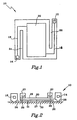
- FIG. 1 and 2 there is shown a conceptual diagram of the microstructure of the present invention.
- a microstructure pixel 10 which is generally of rectangular shape.
- first contact 12 and second contact 14 are used to interconnect with appropriate control circuitry. Oftentimes this control circuitry is located above or below the pixel itself.
- a general description of micromachine pixels as used in infrared applications can be found by referring to B.E. Cole, R.E. Higashi, and R.A. Wood, "Monolith Arrays of Micromachined Pixels for Infrared Applications," Proceedings of the IEEE, Vol. 86, No. 8, pp. 1679-82
- Pixel 10 has a responsive area 20 which is electrically connected to first contact 12 via a resistor path 16. Similarly, responsive area 20 is connected to second contact 14 via a resistive path 18. As will be recognized, responsive area 20 is configured to either emit or detect infrared radiation. Specifically, in an emitter application, current is provided to the responsive area 20 causing responsive area 20 to heat and emit infrared radiation. Conversely, in a detector application responsive area 20 will change its resistance when infrared radiation is encountered. This change in resistance can thus be connected by the associated circuitry and provided to further signal processing systems.
- Pixel 10 further has a first cutout region 22 and a second cutout region 24 to provide appropriate pixel isolation. By providing these cutouts, control of all thermal transfer characteristics is easily achieved.
- FIG 2 there is shown a cross-sectional diagram of the conceptual pixel of figure 1.
- resistive areas 26 are generally deposited and then are completely covered by protective layers 27.
- Protective layers 27 are typically thin film layers of silicon nitride, or a similar compound. It can be seen by referring to figure 2 however, the cross-section of the present pixel is not uniform. More specifically, the portion above responsive region 20 has a reduced cross-section. Such cross-section is created by appropriate thin film processing techniques such as masking, etc.
- This cross-sectional reduction above the active area reduces the overall mass of the pixel itself, having a positive effect on the pixel's operational characteristics. More specifically, the reduction in mass directly affects the time constant of the pixel.
- the time constant is proportionally related to the thermal mass divided by the thermal conductivity of the pixel, this reduction in mass has a direct reduction in the thermal time constant.
- the time constant is inversely proportional to the pixel speed capabilities. Consequently, a reduction in time constant translates into a higher speed pixel.
- the design of the pixel shown in figures 1 and 2 does not in any way compromise the fill factor of the pixel or its optional properties since the IR properties are defined by an absorber layer 29 and a reflector 30.
- the reflective layer may typically consist of a thin metal film such as Pt or Au.
- absorber layer 29 may be fabricated of a thin layer of nickel iron alloy, often called a permalloy. Further discussion regarding optimum configuration and designs for absorber layer 29 and reflector 30 is contained in U.S. Patent No. 5,286,976 entitled Microstructure Design for High IR Sensitivity.
- each pixel is connected to associated control circuitry. This connection is made by having first contact 12 and second contact 14 be connected to supporting elements 28. Supporting elements 28 cause the contacts to stand off a substrate or underlying structure. Within supporting elements 28 are the necessary elements to electrically connect to integrated circuits which are fabricated on a surface below the pixel microstructure 10. This connection structure is commonly referred to as a via which is well understood in the art. Typically coated above the integrated circuits is a reflective coating 30. This reflective coating helps to create a quarter wave resonant cavity beneath the pixel microstructure 10.
- Responsive area 20 existing between the resistor paths 26 has a much lower cross sectional height as shown in figure 2.
- the actual structure of this area includes an absorber layer 29 which is situated on top of a structure layer 31.
- This absorber layer for example could be made of a small thickness of nickel chromium.
- the structure layer 31 however is typically silicon nitrite or some similar material.
- Absorber layer 29 is electrically isolated from the resistive paths for responsive areas.
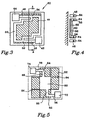
- FIG 3 there is shown pixel 10 again having a first contact 42 and a second contact 44. Attached to each of first contact 42 and second contact 44 is a first resistor leg 46 and a second resistor leg 48 respectively. Each of these resistor legs, 46 and 48, are connected to first contact point 52 and second contact point 54. Connected between first contact point 52 and second contact point 54 are two parallel resistive paths. More specifically, first resistive path 56 progresses from first contact point 52 to second contact point 54 along the right-hand side of the pixel shown in figure 3. Similarly, second resistive path 58 extends from first contact point 52 to second contact point 54 along the left-hand side of the pixel of figure 3.
- Each of these resistive paths create heating structures such that are heated by applying electrical current. This generation of heat is then transmitted to responsive area 60 which is surrounded by first resistive path 56 and second resistive path 58. Heating of these resistive paths also creates heating of the responsive area 60, and in the case of the microemitter the emission of infrared signals.
- first resistive leg 46 second resistive leg 48, first resistive path 56 and second resistive path 58 can be seen.
- protective layers 64 are typically made out of silicon nitride or some other appropriate material.
- the pixel of figure 4 includes an absorber layer 65 and a structure layer 66. In responsive area 60, the only structure remaining are the absorber layer 65 and the structure layer 66.
- absorber layer 65 is typically a thin layer of nickel chromium or some similar material whereas the structure layer is typically silicon nitrite.
- the absorber layer is electrically isolated from the remaining conductors in the pixel, however, helps define the optical properties of the pixel.
- responsive area 60 there currently exists no protective material as this is not necessary. The elimination of the protective layer at this point helps to reduce the overall mass of the pixel itself. It will be appreciated, that a thin protective layer could be included above the responsive area 60.
- Figure 5 displays one possible alternative pixel configuration.
- the pixel of figure 5 includes a first contact 72 and a second contact 74 at opposite comers. Attached to each of these contacts is a first resistor leg 76 and a second resistor leg 78. First, resistor leg 76 extends to a first common point 82 while second resistor leg 78 extends to a second common point 84.
- Each of these structures is substantially similar to that described in relation to figure 3 above.
- a resistor path is created between first common point 82 and second common point 84.
- This resistor path consists primarily of a first resistor lead 86 and a second resistor lead 88 each of which are connected to a central resistor pad 90.
- Surround resistor pad 90 are a plurality of responsive areas 92. As will be appreciated, each of these additional responsive areas 92 are somewhat cantilevered away from the central resistor.
- several reinforcement bars 94 have been incorporated into the design. It will be appreciated that the resistive paths and the central resistive pad will be fully covered by a full height protective layer of silicon nitride whereas the areas above responsive areas 92 will be of a reduced height. Reinforcement bars being of full height silicon nitride material help to strengthen the overall structure. Again, this approach helps to minimize the overall mass of the pixel.
Landscapes
- Physics & Mathematics (AREA)
- General Physics & Mathematics (AREA)
- Spectroscopy & Molecular Physics (AREA)
- Chemical & Material Sciences (AREA)
- Engineering & Computer Science (AREA)
- Nanotechnology (AREA)
- Transforming Light Signals Into Electric Signals (AREA)
- Photometry And Measurement Of Optical Pulse Characteristics (AREA)
- Solid State Image Pick-Up Elements (AREA)
- Outer Garments And Coats (AREA)
- Inorganic Compounds Of Heavy Metals (AREA)
Applications Claiming Priority (3)
| Application Number | Priority Date | Filing Date | Title |
|---|---|---|---|
| US283649 | 1999-04-01 | ||
| US09/283,649 US6046485A (en) | 1999-04-01 | 1999-04-01 | Large area low mass IR pixel having tailored cross section |
| PCT/US2000/006223 WO2000060324A1 (en) | 1999-04-01 | 2000-03-10 | Large area low mass ir pixel having tailored cross section |
Publications (2)
| Publication Number | Publication Date |
|---|---|
| EP1166065A1 EP1166065A1 (en) | 2002-01-02 |
| EP1166065B1 true EP1166065B1 (en) | 2004-06-02 |
Family
ID=23086997
Family Applications (1)
| Application Number | Title | Priority Date | Filing Date |
|---|---|---|---|
| EP00913855A Expired - Lifetime EP1166065B1 (en) | 1999-04-01 | 2000-03-10 | Large area low mass ir pixel having tailored cross section |
Country Status (7)
| Country | Link |
|---|---|
| US (1) | US6046485A (enExample) |
| EP (1) | EP1166065B1 (enExample) |
| JP (1) | JP4700196B2 (enExample) |
| AT (1) | ATE268468T1 (enExample) |
| CA (1) | CA2368974C (enExample) |
| DE (1) | DE60011255T2 (enExample) |
| WO (1) | WO2000060324A1 (enExample) |
Families Citing this family (23)
| Publication number | Priority date | Publication date | Assignee | Title |
|---|---|---|---|---|
| GB2354369A (en) * | 1999-09-17 | 2001-03-21 | Secr Defence | Noise reduced semiconductor photon detectors |
| JP2001153720A (ja) * | 1999-11-30 | 2001-06-08 | Nec Corp | 熱型赤外線検出器 |
| US6649898B1 (en) * | 2000-06-30 | 2003-11-18 | Intel Corporation | Method and apparatus for optically enabling a circuit component in a large scale integrated circuit |
| US6378292B1 (en) * | 2000-11-10 | 2002-04-30 | Honeywell International Inc. | MEMS microthruster array |
| US6559447B2 (en) | 2000-12-26 | 2003-05-06 | Honeywell International Inc. | Lightweight infrared camera |
| US7365326B2 (en) * | 2000-12-26 | 2008-04-29 | Honeywell International Inc. | Camera having distortion correction |
| US6541772B2 (en) | 2000-12-26 | 2003-04-01 | Honeywell International Inc. | Microbolometer operating system |
| US6919730B2 (en) * | 2002-03-18 | 2005-07-19 | Honeywell International, Inc. | Carbon nanotube sensor |
| US7955483B2 (en) * | 2002-03-18 | 2011-06-07 | Honeywell International Inc. | Carbon nanotube-based glucose sensor |
| JP3862080B2 (ja) * | 2002-11-01 | 2006-12-27 | 防衛庁技術研究本部長 | 熱型赤外線検出器の製造方法 |
| US6891161B2 (en) * | 2003-01-17 | 2005-05-10 | Drs Sensors & Targeting Systems, Inc. | Pixel structure and an associated method of fabricating the same |
| DE60308811T2 (de) * | 2003-03-24 | 2007-08-16 | Ihi Aerospace Co., Ltd. | Thermischer Infrarotdetektor mit erhöhtem Füllfaktor, Methode zu dessen Herstellung und Matrix von thermischen Infrarotdetektoren |
| US7170059B2 (en) * | 2003-10-03 | 2007-01-30 | Wood Roland A | Planar thermal array |
| WO2007021030A1 (en) * | 2005-08-17 | 2007-02-22 | Matsushita Electric Works, Ltd. | Infrared sensor unit and process of fabricating the same |
| FR2930639B1 (fr) * | 2008-04-29 | 2011-07-01 | Ulis | Detecteur thermique a haute isolation |
| JP5625232B2 (ja) * | 2008-10-23 | 2014-11-19 | 日本電気株式会社 | 熱型赤外線固体撮像素子 |
| US9250135B2 (en) | 2011-03-16 | 2016-02-02 | Honeywell International Inc. | MWIR sensor for flame detection |
| EP2769407B1 (en) | 2011-10-21 | 2017-05-10 | Santa Barbara Infrared Inc. | Techniques for tiling arrays of pixel elements |
| US9748214B2 (en) | 2011-10-21 | 2017-08-29 | Santa Barbara Infrared, Inc. | Techniques for tiling arrays of pixel elements and fabricating hybridized tiles |
| RU2498103C1 (ru) * | 2012-07-10 | 2013-11-10 | Федеральное государственное бюджетное образовательное учреждение высшего профессионального образования "Московский государственный технический университет имени Н.Э. Баумана" (МГТУ им. Н.Э. Баумана) | Микроэлектромеханический ракетный двигатель |
| WO2016004408A2 (en) * | 2014-07-03 | 2016-01-07 | Flir Systems, Inc. | Vertical microbolometer contact systems and methods |
| US10397947B2 (en) | 2016-08-12 | 2019-08-27 | Qualcomm Incorporated | Adaptive waveform selection in wireless communications |
| EP3938746A2 (en) | 2019-03-11 | 2022-01-19 | Flir Commercial Systems, Inc. | Microbolometer systems and methods |
Family Cites Families (14)
| Publication number | Priority date | Publication date | Assignee | Title |
|---|---|---|---|---|
| US5220188A (en) * | 1983-07-06 | 1993-06-15 | Honeywell Inc. | Integrated micromechanical sensor element |
| US5286976A (en) * | 1988-11-07 | 1994-02-15 | Honeywell Inc. | Microstructure design for high IR sensitivity |
| WO1991016607A1 (en) * | 1990-04-26 | 1991-10-31 | Commonwealth Of Australia, The Secretary Department Of Defence | Semiconductor film bolometer thermal infrared detector |
| US5288649A (en) * | 1991-09-30 | 1994-02-22 | Texas Instruments Incorporated | Method for forming uncooled infrared detector |
| CA2117476C (en) * | 1992-06-19 | 2000-02-22 | R. Andrew Wood | Infrared camera with thermoelectric temperature stabilization |
| JPH07190854A (ja) * | 1993-12-25 | 1995-07-28 | Nippondenso Co Ltd | 赤外線センサ |
| JP2710228B2 (ja) * | 1994-08-11 | 1998-02-10 | 日本電気株式会社 | ボロメータ型赤外線検知素子、その駆動方法、および検出用積分回路 |
| IL115332A0 (en) * | 1994-09-30 | 1995-12-31 | Honeywell Inc | Compact thermal camera |
| US5600148A (en) * | 1994-12-30 | 1997-02-04 | Honeywell Inc. | Low power infrared scene projector array and method of manufacture |
| US5821598A (en) * | 1995-02-01 | 1998-10-13 | Research Corporation Technologies, Inc. | Uncooled amorphous YBaCuO thin film infrared detector |
| JP3811964B2 (ja) * | 1995-02-16 | 2006-08-23 | 三菱電機株式会社 | 赤外線検出装置とその製造方法 |
| FR2752299B1 (fr) * | 1996-08-08 | 1998-09-11 | Commissariat Energie Atomique | Detecteur infrarouge et procede de fabication de celui-ci |
| JPH10122950A (ja) * | 1996-10-23 | 1998-05-15 | Tech Res & Dev Inst Of Japan Def Agency | 熱型赤外線検出器及びその製造方法 |
| US5929441A (en) * | 1997-06-27 | 1999-07-27 | Texas Instruments Incorporated | Low mass optical coating for thin film detectors |
-
1999
- 1999-04-01 US US09/283,649 patent/US6046485A/en not_active Expired - Lifetime
-
2000
- 2000-03-10 EP EP00913855A patent/EP1166065B1/en not_active Expired - Lifetime
- 2000-03-10 DE DE60011255T patent/DE60011255T2/de not_active Expired - Lifetime
- 2000-03-10 JP JP2000609770A patent/JP4700196B2/ja not_active Expired - Lifetime
- 2000-03-10 CA CA002368974A patent/CA2368974C/en not_active Expired - Lifetime
- 2000-03-10 WO PCT/US2000/006223 patent/WO2000060324A1/en not_active Ceased
- 2000-03-10 AT AT00913855T patent/ATE268468T1/de not_active IP Right Cessation
Also Published As
| Publication number | Publication date |
|---|---|
| WO2000060324A1 (en) | 2000-10-12 |
| EP1166065A1 (en) | 2002-01-02 |
| JP2002541449A (ja) | 2002-12-03 |
| JP4700196B2 (ja) | 2011-06-15 |
| ATE268468T1 (de) | 2004-06-15 |
| CA2368974A1 (en) | 2000-10-12 |
| DE60011255D1 (de) | 2004-07-08 |
| CA2368974C (en) | 2009-05-19 |
| DE60011255T2 (de) | 2005-07-07 |
| US6046485A (en) | 2000-04-04 |
Similar Documents
| Publication | Publication Date | Title |
|---|---|---|
| EP1166065B1 (en) | Large area low mass ir pixel having tailored cross section | |
| USRE37146E1 (en) | Low power infrared scene projector array and method of manufacture | |
| US7309865B2 (en) | Electronic device having infrared sensing elements | |
| EP0734589B1 (en) | Integrated silicon vacuum micropackage for infrared devices | |
| US6690014B1 (en) | Microbolometer and method for forming | |
| US4683159A (en) | Semiconductor device structure and processing | |
| US5054936A (en) | Sensor for active thermal detection | |
| US4922116A (en) | Flicker free infrared simulator with resistor bridges | |
| US4888988A (en) | Silicon based mass airflow sensor and its fabrication method | |
| WO2003060441A3 (en) | Sensor device having an integral bi-radial lens | |
| WO2010029488A1 (en) | Planar thermopile infrared microsensor | |
| US7288765B2 (en) | Device for detecting infrared radiation with bolometric detectors | |
| US7604401B2 (en) | Substrate temperature measurement apparatus and processing apparatus | |
| US4739382A (en) | Package for a charge-coupled device with temperature dependent cooling | |
| US6165587A (en) | Microbridge structure with reinforcement section | |
| JP2009003454A (ja) | 温度制御可能な光変調器モジュール及び温度センサ | |
| EP0169519B1 (en) | Semiconductor device and method for its fabrication | |
| JP2007511747A (ja) | プレーナ熱アレイ | |
| JPH06283766A (ja) | 赤外線センサとその製造方法 | |
| US20240272004A1 (en) | Process flow for thin contactless thermal sensors | |
| JPH0953980A (ja) | 熱型赤外線センサ | |
| EP0539355B1 (en) | Flicker-free infrared simulator with resistor bridges | |
| CN117881142A (zh) | 显示设备 | |
| JP2010281947A (ja) | 光導波路デバイス | |
| Carr et al. | Investigating Micromachined Thermal Emitters for Infrared Applications |
Legal Events
| Date | Code | Title | Description |
|---|---|---|---|
| PUAI | Public reference made under article 153(3) epc to a published international application that has entered the european phase |
Free format text: ORIGINAL CODE: 0009012 |
|
| 17P | Request for examination filed |
Effective date: 20011004 |
|
| AK | Designated contracting states |
Kind code of ref document: A1 Designated state(s): AT BE CH CY DE DK ES FI FR GB GR IE IT LI LU MC NL PT SE |
|
| EL | Fr: translation of claims filed | ||
| TCNL | Nl: translation of patent claims filed | ||
| 17Q | First examination report despatched |
Effective date: 20020905 |
|
| GRAP | Despatch of communication of intention to grant a patent |
Free format text: ORIGINAL CODE: EPIDOSNIGR1 |
|
| GRAS | Grant fee paid |
Free format text: ORIGINAL CODE: EPIDOSNIGR3 |
|
| GRAA | (expected) grant |
Free format text: ORIGINAL CODE: 0009210 |
|
| AK | Designated contracting states |
Kind code of ref document: B1 Designated state(s): AT BE CH CY DE DK ES FI FR GB GR IE IT LI LU MC NL PT SE |
|
| PG25 | Lapsed in a contracting state [announced via postgrant information from national office to epo] |
Ref country code: IT Free format text: LAPSE BECAUSE OF FAILURE TO SUBMIT A TRANSLATION OF THE DESCRIPTION OR TO PAY THE FEE WITHIN THE PRESCRIBED TIME-LIMIT;WARNING: LAPSES OF ITALIAN PATENTS WITH EFFECTIVE DATE BEFORE 2007 MAY HAVE OCCURRED AT ANY TIME BEFORE 2007. THE CORRECT EFFECTIVE DATE MAY BE DIFFERENT FROM THE ONE RECORDED. Effective date: 20040602 Ref country code: NL Free format text: LAPSE BECAUSE OF FAILURE TO SUBMIT A TRANSLATION OF THE DESCRIPTION OR TO PAY THE FEE WITHIN THE PRESCRIBED TIME-LIMIT Effective date: 20040602 Ref country code: CH Free format text: LAPSE BECAUSE OF FAILURE TO SUBMIT A TRANSLATION OF THE DESCRIPTION OR TO PAY THE FEE WITHIN THE PRESCRIBED TIME-LIMIT Effective date: 20040602 Ref country code: BE Free format text: LAPSE BECAUSE OF FAILURE TO SUBMIT A TRANSLATION OF THE DESCRIPTION OR TO PAY THE FEE WITHIN THE PRESCRIBED TIME-LIMIT Effective date: 20040602 Ref country code: LI Free format text: LAPSE BECAUSE OF FAILURE TO SUBMIT A TRANSLATION OF THE DESCRIPTION OR TO PAY THE FEE WITHIN THE PRESCRIBED TIME-LIMIT Effective date: 20040602 Ref country code: AT Free format text: LAPSE BECAUSE OF FAILURE TO SUBMIT A TRANSLATION OF THE DESCRIPTION OR TO PAY THE FEE WITHIN THE PRESCRIBED TIME-LIMIT Effective date: 20040602 Ref country code: FI Free format text: LAPSE BECAUSE OF FAILURE TO SUBMIT A TRANSLATION OF THE DESCRIPTION OR TO PAY THE FEE WITHIN THE PRESCRIBED TIME-LIMIT Effective date: 20040602 |
|
| REG | Reference to a national code |
Ref country code: GB Ref legal event code: FG4D |
|
| REG | Reference to a national code |
Ref country code: CH Ref legal event code: EP |
|
| REF | Corresponds to: |
Ref document number: 60011255 Country of ref document: DE Date of ref document: 20040708 Kind code of ref document: P |
|
| REG | Reference to a national code |
Ref country code: IE Ref legal event code: FG4D |
|
| PG25 | Lapsed in a contracting state [announced via postgrant information from national office to epo] |
Ref country code: GR Free format text: LAPSE BECAUSE OF FAILURE TO SUBMIT A TRANSLATION OF THE DESCRIPTION OR TO PAY THE FEE WITHIN THE PRESCRIBED TIME-LIMIT Effective date: 20040902 Ref country code: DK Free format text: LAPSE BECAUSE OF FAILURE TO SUBMIT A TRANSLATION OF THE DESCRIPTION OR TO PAY THE FEE WITHIN THE PRESCRIBED TIME-LIMIT Effective date: 20040902 Ref country code: SE Free format text: LAPSE BECAUSE OF FAILURE TO SUBMIT A TRANSLATION OF THE DESCRIPTION OR TO PAY THE FEE WITHIN THE PRESCRIBED TIME-LIMIT Effective date: 20040902 |
|
| PG25 | Lapsed in a contracting state [announced via postgrant information from national office to epo] |
Ref country code: ES Free format text: LAPSE BECAUSE OF FAILURE TO SUBMIT A TRANSLATION OF THE DESCRIPTION OR TO PAY THE FEE WITHIN THE PRESCRIBED TIME-LIMIT Effective date: 20040913 |
|
| REG | Reference to a national code |
Ref country code: CH Ref legal event code: PL |
|
| NLV1 | Nl: lapsed or annulled due to failure to fulfill the requirements of art. 29p and 29m of the patents act | ||
| ET | Fr: translation filed | ||
| PG25 | Lapsed in a contracting state [announced via postgrant information from national office to epo] |
Ref country code: IE Free format text: LAPSE BECAUSE OF NON-PAYMENT OF DUE FEES Effective date: 20050310 Ref country code: CY Free format text: LAPSE BECAUSE OF FAILURE TO SUBMIT A TRANSLATION OF THE DESCRIPTION OR TO PAY THE FEE WITHIN THE PRESCRIBED TIME-LIMIT Effective date: 20050310 Ref country code: LU Free format text: LAPSE BECAUSE OF NON-PAYMENT OF DUE FEES Effective date: 20050310 |
|
| PG25 | Lapsed in a contracting state [announced via postgrant information from national office to epo] |
Ref country code: MC Free format text: LAPSE BECAUSE OF NON-PAYMENT OF DUE FEES Effective date: 20050331 |
|
| PLBE | No opposition filed within time limit |
Free format text: ORIGINAL CODE: 0009261 |
|
| STAA | Information on the status of an ep patent application or granted ep patent |
Free format text: STATUS: NO OPPOSITION FILED WITHIN TIME LIMIT |
|
| 26N | No opposition filed |
Effective date: 20050303 |
|
| REG | Reference to a national code |
Ref country code: IE Ref legal event code: MM4A |
|
| PG25 | Lapsed in a contracting state [announced via postgrant information from national office to epo] |
Ref country code: PT Free format text: LAPSE BECAUSE OF NON-PAYMENT OF DUE FEES Effective date: 20041102 |
|
| REG | Reference to a national code |
Ref country code: FR Ref legal event code: PLFP Year of fee payment: 17 |
|
| REG | Reference to a national code |
Ref country code: FR Ref legal event code: PLFP Year of fee payment: 18 |
|
| REG | Reference to a national code |
Ref country code: FR Ref legal event code: PLFP Year of fee payment: 19 |
|
| PGFP | Annual fee paid to national office [announced via postgrant information from national office to epo] |
Ref country code: GB Payment date: 20190327 Year of fee payment: 20 Ref country code: FR Payment date: 20190328 Year of fee payment: 20 |
|
| PGFP | Annual fee paid to national office [announced via postgrant information from national office to epo] |
Ref country code: DE Payment date: 20190411 Year of fee payment: 20 |
|
| REG | Reference to a national code |
Ref country code: DE Ref legal event code: R071 Ref document number: 60011255 Country of ref document: DE |
|
| REG | Reference to a national code |
Ref country code: GB Ref legal event code: PE20 Expiry date: 20200309 |
|
| PG25 | Lapsed in a contracting state [announced via postgrant information from national office to epo] |
Ref country code: GB Free format text: LAPSE BECAUSE OF EXPIRATION OF PROTECTION Effective date: 20200309 |