EP1163721B1 - Filter for digital to analog converters - Google Patents
Filter for digital to analog converters Download PDFInfo
- Publication number
- EP1163721B1 EP1163721B1 EP00918174.4A EP00918174A EP1163721B1 EP 1163721 B1 EP1163721 B1 EP 1163721B1 EP 00918174 A EP00918174 A EP 00918174A EP 1163721 B1 EP1163721 B1 EP 1163721B1
- Authority
- EP
- European Patent Office
- Prior art keywords
- digital
- filter
- frequency response
- signal
- digital signal
- Prior art date
- Legal status (The legal status is an assumption and is not a legal conclusion. Google has not performed a legal analysis and makes no representation as to the accuracy of the status listed.)
- Expired - Lifetime
Links
- 230000004044 response Effects 0.000 claims description 156
- 238000012937 correction Methods 0.000 claims description 50
- 230000007704 transition Effects 0.000 claims description 43
- 238000000034 method Methods 0.000 claims description 37
- 238000012545 processing Methods 0.000 claims description 37
- 238000005070 sampling Methods 0.000 claims description 19
- 239000006185 dispersion Substances 0.000 claims description 16
- 238000001914 filtration Methods 0.000 claims description 14
- 238000013144 data compression Methods 0.000 claims description 7
- 230000000694 effects Effects 0.000 claims description 7
- 238000007726 management method Methods 0.000 claims description 3
- 239000012636 effector Substances 0.000 claims 3
- 238000010586 diagram Methods 0.000 description 9
- 238000006243 chemical reaction Methods 0.000 description 7
- 238000013461 design Methods 0.000 description 7
- 230000006870 function Effects 0.000 description 5
- 230000008569 process Effects 0.000 description 5
- 238000012360 testing method Methods 0.000 description 4
- 238000013459 approach Methods 0.000 description 3
- 230000000295 complement effect Effects 0.000 description 2
- 239000002131 composite material Substances 0.000 description 2
- 230000006872 improvement Effects 0.000 description 2
- 230000007246 mechanism Effects 0.000 description 2
- 230000005236 sound signal Effects 0.000 description 2
- 230000001052 transient effect Effects 0.000 description 2
- XUIMIQQOPSSXEZ-UHFFFAOYSA-N Silicon Chemical compound [Si] XUIMIQQOPSSXEZ-UHFFFAOYSA-N 0.000 description 1
- 238000004458 analytical method Methods 0.000 description 1
- 230000008901 benefit Effects 0.000 description 1
- 230000008859 change Effects 0.000 description 1
- 238000007906 compression Methods 0.000 description 1
- 230000006835 compression Effects 0.000 description 1
- 238000013500 data storage Methods 0.000 description 1
- 239000000463 material Substances 0.000 description 1
- 238000012986 modification Methods 0.000 description 1
- 230000004048 modification Effects 0.000 description 1
- 230000007935 neutral effect Effects 0.000 description 1
- 238000009527 percussion Methods 0.000 description 1
- 230000010363 phase shift Effects 0.000 description 1
- 230000009467 reduction Effects 0.000 description 1
- 229910052710 silicon Inorganic materials 0.000 description 1
- 239000010703 silicon Substances 0.000 description 1
- 230000007480 spreading Effects 0.000 description 1
- 239000002023 wood Substances 0.000 description 1
Images


Classifications
-
- H—ELECTRICITY
- H03—ELECTRONIC CIRCUITRY
- H03H—IMPEDANCE NETWORKS, e.g. RESONANT CIRCUITS; RESONATORS
- H03H17/00—Networks using digital techniques
- H03H17/02—Frequency selective networks
- H03H17/06—Non-recursive filters
- H03H17/0621—Non-recursive filters with input-sampling frequency and output-delivery frequency which differ, e.g. extrapolation; Anti-aliasing
Definitions
- the invention relates generally to improvements in digital-to-analog (D-to-A) conversion, and, more particularly, to improvements in such conversion for audio signals. It is most useful in high quality audio for music reproduction in devices such as Compact Disc (CD) players, DVD players, etc.
- D-to-A digital-to-analog
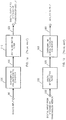
- FIG. J a is a simplified block diagram of an A-to-D converter and FIG. 1b is a simplified block diagram of a corresponding D-to-A converter.
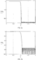
- FIG. 2a shows the frequency response of a typical filter used in an A-to-D converter as the final decimation filter.
- FIG. 2b shows the response of a typical filter used in a D-to-A converter as the first interpolation filter.
- the Y-axis of the graphs shows the magnitude of the amplitude response of the filters in decibels
- the X-axis shows the frequency as a fraction of the output/input sampling rate, Fs.
- the incoming digital signal 122 ( FIG. 1b ) can be considered to have no frequencies above 0.5 Fs.
- the first stage of interpolation consists of adding zero value samples in between each of the original samples to double the sample rate and then passing the result through a low pass filter with a frequency response such as in FIG. 2b . The result is that the zero valued samples are replaced by values that are interpolated from the surrounding data.
- the distortion arises from the fact that new frequencies are created above the original Nyquist frequency and that these new frequencies correspond to frequencies present in the original signal.
- it is useful to graph the composite frequency response of the decimation/interpolation system. If one takes the frequency response of the A-to-D decimation filter in FIG. 2a and performs the equivalent decimation followed by inserting the zero value samples prior to the interpolation filter, one gets a frequency response shown in FIG. 3a . For each frequency below the Nyquist 200, a new frequency above Nyquist is created.
- f_new equals FS-f
- f_new alias products have in the A-to-D case, as can be seen from the symmetry about Nyquist 200.
- f_new new frequencies
- the frequencies above 0.5 are signals which were not there in the original signal and are alias distortion products. They fall into two general groups: those corresponding to the stop band of the interpolation filter 220, and those associated with the transition band behavior of both the decimation and interpolation filters 210.
- the acceptable level of stop band distortion products 220 determine the stop band performance requirement for the interpolation filter. The only way to reduce these distortions is to improve the performance of the interpolation filter stop band rejection.
- the transition band distortions at 210 are more limited in frequency range, but they have much higher amplitude and can cause really audible problems in the output of a system.
- a cymbal crash in music which generates large amplitude high frequency components.
- For each component just below Nyquist there is a corresponding one at a mirror image frequency above Nyquist, and each pair of original frequency and alias frequency will generate a difference component when it encounters a non-linearity later in the system.
- these difference components are in the frequency range of 0 to 5 kilohertz, where human hearing is very sensitive and where they are not masked very well by the signal that created them. They result in a "dirty" sound to the cymbals, which is very typical of digital systems.
- Transition band distortions 210 result primarily from the transition band behavior of the interpolation filter.
- the type of filter that is normally used in this position in a system design is called a half-band filter. As can be seen from FIG. 2b , it is 6 dB down at Nyquist with considerable response above the 0.5 frequency.
- FIR finite impulse response
- the first disadvantage is cost.
- the complexity of a non-half-band filter appropriate for this application is usually more than twice as great as the corresponding conventional half-band filter. This translates directly into silicon area, and hence cost, in a hardware implementation.
- the second disadvantage is that the output sample rate of the better interpolation filter is two times the Fs of the input and a D-to-A converter following the filter must be able to accept the higher sampling rate. Since most converters used in modem equipment are really combination filter/D-to-A converters they may not accept the higher sample rate.
- the present invention provides a method for and a system of processing a digitally encoded signal that eliminates a type of alias distortion arising from the transition band behavior of half-band interpolation filters commonly used in D-to-A converters.
- the invention also provides a method for designing filters that reduce alias distortion for use with D-to-A converters.
- the method for processing a digitally encoded signal converted from an analog signal using a digital decimation filter having an associated frequency response includes the steps of filtering the digital signal through a digital interpolation filter having an associated frequency response, wherein the digital interpolation filter is a half-band interpolation filter; prior to filtering the digital signal through the digital interpolation filter, locating the transition band portion of the frequency response resulting from the combination of the digital decimation filter frequency response and the digital interpolation filter frequency response; and attenuating the digital signal in the frequency range of the transition band portion.
- the method substantially eliminates the transition-band alias distortion associated with presently known D-to-A conversion processes without altering the interpolation filtering process itself.
- the method further includes the step of performing additional signal processing on the digital signal after the step of attenuating the digital signal in the frequency range of the transition band portion.
- the method further includes the steps of performing data compression on the digital signal after filtering the digital signal using the digital decimation filter; and subsequently performing data expansion of the digital signal prior to the step of attenuating the digital signal in the frequency range of the transition band portion.
- the system for processing a digital signal converted from an analog signal using a digital decimation filter having an associated frequency response includes a digital interpolation filter having an associated frequency response, the digital interpolation filter being a half-band interpolation filter; and an alias correction filter responsive to the digital signal for producing an alias-corrected signal, said alias correction filter having a frequency response that attenuates the digital signal in the frequency range of the transition band portion of the frequency response resulting from the combination of the digital decimation filter frequency response and the digital interpolation filter frequency response, wherein the digital interpolation filter is responsive to the alias-corrected signal for producing an interpolated digital signal.
- the digital decimation filter includes a series of individual digital decimation filters and the transition band portion of the frequency response is present within the frequency response resulting from the combination of the frequency response of the last digital decimation filter in the decimation-filter series and the digital interpolation filter frequency response.
- the digital interpolation filter includes a series of individual digital interpolation filters and the transition band portion of the frequency response is present within the frequency response resulting from the combination of the frequency response of the first digital interpolation filter in the interpolation-filter series and the digital decimation filter frequency response.
- the system further includes a signal processor responsive to the alias corrected signal for providing a processed alias-corrected signal.
- the system further includes a data compressor responsive to the decimated digital signal for performing data compression on the signal and a data expander responsive to the compressed decimated digital signal for performing data expansion on the signal.
- the digital signal being subsequently converted to an output analog using a digital-to-analog converter comprising a digital interpolation filter.
- Each of the decimation and interpolation filters have an associated frequency response.
- the method includes the steps of a) locating a transition band portion of the frequency response resulting from the combination of the digital decimation filter frequency response and the digital interpolation filter frequency response; b) selecting a first attenuation filter having a first frequency response that attenuates the digital signal in the frequency range of the distortion band portion; c) convolving the impulse responses of the decimation filter and the interpolation filter to produce a first impulse response; and d) convolving the impulse responses of the decimation filter, the attenuation filter and the interpolation filter to produce a second impulse response.
- the method further includes the steps of e) comparing the time dispersion of the second impulse response in a region of the second impulse response above minus 80 dB with the time dispersion of the first impulse response in the same region; f) if the width of the second-impulse-response time dispersion in the region is greater than the width of the first-impulse-response time dispersion in the same region, selecting another attenuation filter having a frequency response different then the first frequency response, that attenuates the digital signal in the frequency range of the transition band portion; and g) repeating steps d, e and f until the width of the second-impulse-response time dispersion in the region is no greater than the width of the first-impulse-response time dispersion in the same region.
- the invention can eliminate the alias distortion associated with D-to-A converters without significantly changing the time-domain response of the system.
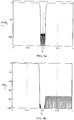
- the convolved impulse response is plotted on a logarithmic scale.
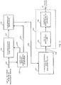
- FIG. 4 shows a D-to-A converter system according to the invention.
- the original D-to-A converter structure is shown enclosed in a dashed line 140, and in many commercial applications, several channels of this type are integrated on a single integrated circuit (IC).
- the added filter 130 is placed in the input stream to the original converter. This filter 130 is referred to herein as an "1xFs alias correction filter.” It is important to note that the input 122 and the output 135 of the alias correction filter 130 are at the same sample rate Fs and that is why it is called a 1xFs alias correction filter.
- the frequency response of a typical instance of this filter is shown in FIG. 5a . It is a low-pass filter that attenuates only the frequencies in the input signal which are very near Nyquist.
- the plot of the filter is shown with the zero samples inserted, ready for interpolation, to make its relationship to the other plots clearer.
- the instance of the filter that is shown is a symmetrical FIR filter, which has linear phase response. Because it is operating at Fs, only the frequency response up to 0.5 Fs is necessary to specify its behavior.
- the alias response 220 ( FIG. 3b ) corresponding to the stop-band of the interpolation filter is not altered by the added alias correction filter 130, since a filter operating at 1xFs cannot change that area of the response while maintaining in-band performance.
- the only way that the stop-band related problems could be fixed is by using a filter at a higher sampling rate.
- transition band alias distortion 210 is much more audible than the higher frequency, lower amplitude distortions from the stop-band range 220.
- the introduction of the alias correction filter 130 can dramatically improve the sound of the system.
- the added alias correction filter 130 is a low-pass filter.
- the loss of frequencies at about 20 kilohertz and higher is not usually sonically significant.
- time smear Another phenomenon which may sound like the loss of high frequency resolution that is actually caused by a different mechanism having to do with dispersion of transient energy over time.
- FIG. 6a A plot of this type for a simple decimation and interpolation filter combination like FIG. 3b is plotted in FIG. 6a .
- the vertical axis is the amplitude in dB with reference to full scale, and the horizontal axis is in samples. This can be thought of as the response of the system in time to a single impulse of unity amplitude (0 dB). Notice that the energy in the system response to a single impulse spike is spread over many samples in time.
- the spread in time at the point where the plot is 50 dB below full scale is about 3 milliseconds. This time corresponds to physical dimensions of roughly one meter, given the speed of sound in air. If the source of the sound was originally smaller, such as a wood block percussion instrument, the spreading in time or time smear will alter the sound as reproduced by the system in a way that sounds like a loss of high frequency resolution.
- the plot in FIG. 6b is the same decimation/interpolation filter pair as in FIG 6a , cascaded with the alias correction filter of FIG. 5a . Notice that the width of the plot above -75 dB in FIG. 6b is narrower than the corresponding section of Fig 6a .
- the combination of filters in FIG. 6b actually sounds as if it has better high frequency response than FIG. 6a even though it actually has less high frequency components because of the low pass filter. It also sounds much less distorted because the alias distortion from the transition region has been suppressed.
- the combination of the 1xFs alias correction filter 130 with a half-band interpolation filter 150 and D-to-A converter 160 is frequently more economical to implement than the more complex non-half-band filter approach of the prior art.
- DSP digital signal processing
- Examples are DVD players and A/V receivers that use DSP functions to decode compressed audio and for other functions such as bass management.
- DSP digital signal processing
- the invention allows systems designers to use the same standard integrated filter/D-to-A converter and gain the advantage of a better quality conversion with lower alias distortion.
- alias correction filter 130 at the input sampling frequency of a D-to-A converter to reduce its alias distortion is believed to be new and novel.
- transition band alias distortions 210 does not seem to be well understood in the current literature, and is not reflected in current system designs except those employing HDCD, i. e., the prior cited U.S. patents.
- the method of analysis of the frequency and time domain behavior of cascaded decimation/interpolation filter systems set forth above and its use in designing interpolation filters or alias correction filters is believed to be unique.
- alias correction filter 130 connected directly to the interpolation filter 150 and D-to-A converter 160.
- the basic structure of the invention There are many possible variations of the basic structure of the invention that have the same basic functionality.
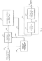
- FIG. 7 One possible variation is shown in FIG. 7 .
- the alias correction filter 130 is inserted in the data stream at the input 122 and then other digital processing 137 is done on the signal before it goes to the interpolation filter.
- This other processing 137 can include bass management, spatial effects, tone controls, reverb, etc. without changing the essence of the invention. Since the behavior of the alias correction is based on the cascaded filters of the system, adding other processing is possible anywhere in the chain without altering the basic behavior of the corrective effect.
- FIG. 8 Yet another example is shown in FIG. 8 .
- This is an example of systems in which some form of data compression is used to achieve a higher data storage density. Examples of such systems are AC3, MPEG audio compression, etc.
- the section of the playback system 125 responsible for decoding or expanding the compressed format must precede the alias correction filter 130. This block may also include other processing before the alias correction filter.
- FIG. 9 shows an example of a form of HDCD system according to, the prior art described in the previously referenced U.S. patents.
- the decimation filter used in the encoder is selected dynamically for best fidelity based on the content of the program material. Since the alias correction filter 130 design is optimally based on both the decimation filter and the interpolation filter 150 used, and since the choice of decimation filter is conveyed to the reproducer via a hidden code side channel, the alias correction filter can be selected dynamically to give the best complement to the decimation filter at any given time. This is accomplished by a hidden code/filter select device 128, which recovers the hidden code information, decodes the commands contained in the hidden code, and selects one of several alias correction filters 130 using a control signal 129.
- FIG. 10 is another example of an HDCD system similar to FIG. 9 with the addition of the HDCD amplitude decoder 125.
- the function of the amplitude decoder is also controlled by the hidden code side channel via the code command decoder 128 and control signal 126.
- the amplitude decoding must be done before the alias correction filter 130 in order for the decoding to track the encoding properly.
- the alias correction filter 130 described above is a symmetrical FIR filter, which has linear phase characteristics
- other types of filters could be used to accomplish the same goal.
- One possible type is a minimum phase IIR (infinite impulse response) filter. This type of filter has the time domain characteristic that the filter ringing occurs after the transient event that caused it. This would probably have a better time domain behavior from an audibility standpoint, although the phase shift near the band edge might cause other perceptual problems.
- the example filters used in the discussion so far have been designs used for CD players and other systems with sampling rates between 40 and 50 kHz.
- the invention is also useful for high-resolution systems with higher sampling rates, such as DVD Audio, which allows sampling rates up to 192 kHz.
- sampling rate is increased by an octave or two
- the transition band alias 210 problems are still an issue.
- Half-band interpolation filters are still the norm for most audio systems designs, and the signal frequency component-alias frequency component pairs can still cause difference frequencies in the audio band when they encounter non-linearities down stream in the system. This is true even though the amplitude of audio signals is lower in the transition region of the filters at higher sampling frequencies.
Landscapes
- Physics & Mathematics (AREA)
- Engineering & Computer Science (AREA)
- Computer Hardware Design (AREA)
- Mathematical Physics (AREA)
- Analogue/Digital Conversion (AREA)
- Compression, Expansion, Code Conversion, And Decoders (AREA)
Applications Claiming Priority (5)
| Application Number | Priority Date | Filing Date | Title |
|---|---|---|---|
| US12572699P | 1999-03-23 | 1999-03-23 | |
| US125726P | 1999-03-23 | ||
| US09/521,503 US6337645B1 (en) | 1999-03-23 | 2000-03-09 | Filter for digital-to-analog converters |
| US521503 | 2000-03-09 | ||
| PCT/US2000/007407 WO2000057549A1 (en) | 1999-03-23 | 2000-03-21 | Filter for digital to analog converters |
Publications (2)
| Publication Number | Publication Date |
|---|---|
| EP1163721A1 EP1163721A1 (en) | 2001-12-19 |
| EP1163721B1 true EP1163721B1 (en) | 2017-01-04 |
Family
ID=26823874
Family Applications (1)
| Application Number | Title | Priority Date | Filing Date |
|---|---|---|---|
| EP00918174.4A Expired - Lifetime EP1163721B1 (en) | 1999-03-23 | 2000-03-21 | Filter for digital to analog converters |
Country Status (8)
| Country | Link |
|---|---|
| US (1) | US6337645B1 (enExample) |
| EP (1) | EP1163721B1 (enExample) |
| JP (1) | JP4469090B2 (enExample) |
| AU (1) | AU3903400A (enExample) |
| HK (1) | HK1042787B (enExample) |
| MY (1) | MY125215A (enExample) |
| TW (1) | TW457781B (enExample) |
| WO (1) | WO2000057549A1 (enExample) |
Families Citing this family (13)
| Publication number | Priority date | Publication date | Assignee | Title |
|---|---|---|---|---|
| US7133569B1 (en) * | 2000-07-31 | 2006-11-07 | Polaroid Corporation | Aliasing artifact attenuation system |
| US6462690B1 (en) * | 2001-04-02 | 2002-10-08 | Cirrus Logic, Inc. | Circuit systems and methods for multirate digital-to-analog amplifier systems |
| US6639526B1 (en) * | 2002-03-21 | 2003-10-28 | Linear Technology Corporation | Circuits and methods for a variable oversample ratio delta-sigma analog-to-digital converter |
| JP2005287820A (ja) * | 2004-03-31 | 2005-10-20 | U-Medica Inc | 生体現象測定記録装置及びノイズ成分除去方法 |
| KR100914159B1 (ko) | 2007-11-21 | 2009-08-28 | 포스데이타 주식회사 | 무선통신 시스템에서의 디지털 주파수 업 변환 장치 및방법 |
| WO2009066954A2 (en) * | 2007-11-21 | 2009-05-28 | Posdata Co., Ltd. | Apparatus and method for up-converting frequency in wireless communication system |
| US8539113B2 (en) | 2011-06-16 | 2013-09-17 | Hewlett-Packard Development Company, L.P. | Indicators for streams associated with messages |
| US9094032B2 (en) * | 2011-07-20 | 2015-07-28 | Freescale Semiconductor, Inc. | Integrated circuit device and method of dynamically modifying at least one characteristic within a digital to analogue converter module |
| US8599050B2 (en) | 2012-01-06 | 2013-12-03 | Maxlinear, Inc. | Method and system for broadband analog to digital converter technology |
| GB201300309D0 (en) * | 2013-01-08 | 2013-02-20 | Meridian Audio Ltd | Digital encapsulation of audio signals |
| EP4002359B1 (en) | 2014-06-10 | 2025-09-03 | Lenbrook Industries Limited | Digital encapsulation of audio signals |
| CN105553444B (zh) * | 2015-12-15 | 2017-12-05 | 一诺仪器(中国)有限公司 | 自适应滤波器 |
| TWI717659B (zh) * | 2018-11-20 | 2021-02-01 | 新唐科技股份有限公司 | 訊號處理系統及其方法 |
Family Cites Families (14)
| Publication number | Priority date | Publication date | Assignee | Title |
|---|---|---|---|---|
| US5235534A (en) * | 1988-08-18 | 1993-08-10 | Hewlett-Packard Company | Method and apparatus for interpolating between data samples |
| US5079734A (en) * | 1990-04-30 | 1992-01-07 | Harris Corporation | Digital decimation filter |
| AU669114B2 (en) | 1991-05-29 | 1996-05-30 | Pacific Microsonics, Inc. | Improved signal encode/decode system |
| GB2262854B (en) * | 1991-12-24 | 1995-05-24 | Sony Broadcast & Communication | Image processing apparatus |
| US5561424A (en) * | 1993-04-30 | 1996-10-01 | Lucent Technologies Inc. | Data converter with minimum phase fir filter and method for calculating filter coefficients |
| US5963160A (en) * | 1993-09-13 | 1999-10-05 | Analog Devices, Inc. | Analog to digital conversion using nonuniform sample rates |
| RU2171007C2 (ru) * | 1993-11-09 | 2001-07-20 | Моторола, Инк. | Детектор уровня и способ детектирования уровня входного сигнала |
| US5450083A (en) | 1994-03-09 | 1995-09-12 | Analog Devices, Inc. | Two-stage decimation filter |
| US5529068A (en) * | 1994-06-16 | 1996-06-25 | The Regents Of The University Of California | Synchronized digital signal processor for MRI reception |
| DE59409276D1 (de) * | 1994-08-08 | 2000-05-11 | Micronas Intermetall Gmbh | Verfahren zur digitalen Interpolation von Signalen |
| US5657261A (en) * | 1995-04-17 | 1997-08-12 | Wilson; Dennis L. | Interpolation of digital signals using signal sample replication |
| JP3327114B2 (ja) * | 1996-04-24 | 2002-09-24 | ソニー株式会社 | 信号処理装置、信号記録装置及び信号再生装置 |
| US5781137A (en) * | 1996-12-23 | 1998-07-14 | National Instruments Corporation | System and method for reducing errors in a delta-sigma converter |
| US5935199A (en) * | 1997-06-27 | 1999-08-10 | Cirrus Logic, Inc. | Dc accurate multi-rate digital filter with common coefficient set and dc gain correction |
-
2000
- 2000-03-09 US US09/521,503 patent/US6337645B1/en not_active Expired - Lifetime
- 2000-03-21 HK HK02104477.2A patent/HK1042787B/en not_active IP Right Cessation
- 2000-03-21 EP EP00918174.4A patent/EP1163721B1/en not_active Expired - Lifetime
- 2000-03-21 WO PCT/US2000/007407 patent/WO2000057549A1/en not_active Ceased
- 2000-03-21 JP JP2000607328A patent/JP4469090B2/ja not_active Expired - Fee Related
- 2000-03-21 AU AU39034/00A patent/AU3903400A/en not_active Abandoned
- 2000-03-22 TW TW089105218A patent/TW457781B/zh not_active IP Right Cessation
- 2000-03-23 MY MYPI20001153A patent/MY125215A/en unknown
Non-Patent Citations (1)
| Title |
|---|
| KEITH O JOHNSON ET AL: "COMPATIBLE RESOLUTION ENHANCEMENT IN DIGITAL AUDIO SYSTEMS", AES, 1 November 1996 (1996-11-01), XP055160704 * |
Also Published As
| Publication number | Publication date |
|---|---|
| HK1042787B (en) | 2018-03-09 |
| JP4469090B2 (ja) | 2010-05-26 |
| EP1163721A1 (en) | 2001-12-19 |
| JP2002540667A (ja) | 2002-11-26 |
| MY125215A (en) | 2006-07-31 |
| AU3903400A (en) | 2000-10-09 |
| TW457781B (en) | 2001-10-01 |
| US6337645B1 (en) | 2002-01-08 |
| WO2000057549A1 (en) | 2000-09-28 |
Similar Documents
| Publication | Publication Date | Title |
|---|---|---|
| EP1163721B1 (en) | Filter for digital to analog converters | |
| CA2506118C (en) | Electronic signal encoding and decoding | |
| AU2012202127B2 (en) | System and method for digital signal processing | |
| HK1042787A (en) | Filter for digital to analog converters | |
| EP1430475A1 (en) | Bandwidth extension of a sound signal | |
| KR20070011534A (ko) | 워핑된 처리를 이용한 디지털 오디오의 동적 범위 제어 및등화 | |
| US20020173865A1 (en) | Digital audio signal processing | |
| EP0497050B1 (en) | PCM digital audio signal playback apparatus | |
| US5805715A (en) | Method and apparatus for compensating multi-resolution linear distortion | |
| EP1722360A1 (en) | Audio enhancement system and method | |
| US8160887B2 (en) | Adaptive interpolation in upsampled audio signal based on frequency of polarity reversals | |
| EP1374632A2 (en) | A method of modifying low frequency components of a digital audio signal | |
| JPH0771359B2 (ja) | マルチウエイスピ−カ装置用ネツトワ−ク | |
| CN1267960A (zh) | 用于数模转换器的滤波器 | |
| JP2000349579A (ja) | デジタルオーディオ用帯域制限アナログフィルタ及びこれを用いた音声信号増幅装置 | |
| JP3297792B2 (ja) | 信号伸張装置及び方法 | |
| JP4364599B2 (ja) | フィルタ処理装置,フィルタ処理方法及びそのプログラム | |
| JP3495581B2 (ja) | 信号処理回路 | |
| JP2832780B2 (ja) | エコー付加回路を有するオーディオ装置 | |
| JP2507285B2 (ja) | ビット長拡張装置 | |
| WO2001039174A1 (en) | Low memory digital audio effects using down-sampling up-sampling technique | |
| JPS63300699A (ja) | マルチウェイスピ−カ装置用ネットワ−ク | |
| KR20050093408A (ko) | 음성신호 처리 장치 및 그 동작방법 | |
| JPS6229219A (ja) | アナログ信号の標本化回路 | |
| JPH05235674A (ja) | ディジタル増幅器 |
Legal Events
| Date | Code | Title | Description |
|---|---|---|---|
| PUAI | Public reference made under article 153(3) epc to a published international application that has entered the european phase |
Free format text: ORIGINAL CODE: 0009012 |
|
| 17P | Request for examination filed |
Effective date: 20010907 |
|
| AK | Designated contracting states |
Kind code of ref document: A1 Designated state(s): AT BE CH CY DE DK ES FI FR GB GR IE IT LI LU MC NL PT SE |
|
| AX | Request for extension of the european patent |
Free format text: AL PAYMENT 20010907;LT PAYMENT 20010907;LV PAYMENT 20010907;MK PAYMENT 20010907;RO PAYMENT 20010907;SI PAYMENT 20010907 |
|
| RAP1 | Party data changed (applicant data changed or rights of an application transferred) |
Owner name: MICROSOFT CORPORATION |
|
| 17Q | First examination report despatched |
Effective date: 20080910 |
|
| RAP1 | Party data changed (applicant data changed or rights of an application transferred) |
Owner name: MICROSOFT TECHNOLOGY LICENSING, LLC |
|
| GRAP | Despatch of communication of intention to grant a patent |
Free format text: ORIGINAL CODE: EPIDOSNIGR1 |
|
| INTG | Intention to grant announced |
Effective date: 20160715 |
|
| GRAS | Grant fee paid |
Free format text: ORIGINAL CODE: EPIDOSNIGR3 |
|
| GRAA | (expected) grant |
Free format text: ORIGINAL CODE: 0009210 |
|
| AK | Designated contracting states |
Kind code of ref document: B1 Designated state(s): AT BE CH CY DE DK ES FI FR GB GR IE IT LI LU MC NL PT SE |
|
| AX | Request for extension of the european patent |
Extension state: AL LT LV MK RO SI |
|
| REG | Reference to a national code |
Ref country code: GB Ref legal event code: FG4D |
|
| REG | Reference to a national code |
Ref country code: CH Ref legal event code: EP |
|
| REG | Reference to a national code |
Ref country code: AT Ref legal event code: REF Ref document number: 860143 Country of ref document: AT Kind code of ref document: T Effective date: 20170115 |
|
| REG | Reference to a national code |
Ref country code: IE Ref legal event code: FG4D |
|
| REG | Reference to a national code |
Ref country code: FR Ref legal event code: PLFP Year of fee payment: 18 |
|
| REG | Reference to a national code |
Ref country code: DE Ref legal event code: R096 Ref document number: 60049525 Country of ref document: DE |
|
| REG | Reference to a national code |
Ref country code: NL Ref legal event code: FP |
|
| REG | Reference to a national code |
Ref country code: LT Ref legal event code: MG9D |
|
| REG | Reference to a national code |
Ref country code: AT Ref legal event code: MK05 Ref document number: 860143 Country of ref document: AT Kind code of ref document: T Effective date: 20170104 |
|
| PG25 | Lapsed in a contracting state [announced via postgrant information from national office to epo] |
Ref country code: GR Free format text: LAPSE BECAUSE OF FAILURE TO SUBMIT A TRANSLATION OF THE DESCRIPTION OR TO PAY THE FEE WITHIN THE PRESCRIBED TIME-LIMIT Effective date: 20170405 Ref country code: FI Free format text: LAPSE BECAUSE OF FAILURE TO SUBMIT A TRANSLATION OF THE DESCRIPTION OR TO PAY THE FEE WITHIN THE PRESCRIBED TIME-LIMIT Effective date: 20170104 |
|
| PG25 | Lapsed in a contracting state [announced via postgrant information from national office to epo] |
Ref country code: ES Free format text: LAPSE BECAUSE OF FAILURE TO SUBMIT A TRANSLATION OF THE DESCRIPTION OR TO PAY THE FEE WITHIN THE PRESCRIBED TIME-LIMIT Effective date: 20170104 Ref country code: SE Free format text: LAPSE BECAUSE OF FAILURE TO SUBMIT A TRANSLATION OF THE DESCRIPTION OR TO PAY THE FEE WITHIN THE PRESCRIBED TIME-LIMIT Effective date: 20170104 Ref country code: PT Free format text: LAPSE BECAUSE OF FAILURE TO SUBMIT A TRANSLATION OF THE DESCRIPTION OR TO PAY THE FEE WITHIN THE PRESCRIBED TIME-LIMIT Effective date: 20170504 Ref country code: AT Free format text: LAPSE BECAUSE OF FAILURE TO SUBMIT A TRANSLATION OF THE DESCRIPTION OR TO PAY THE FEE WITHIN THE PRESCRIBED TIME-LIMIT Effective date: 20170104 |
|
| REG | Reference to a national code |
Ref country code: DE Ref legal event code: R097 Ref document number: 60049525 Country of ref document: DE |
|
| PG25 | Lapsed in a contracting state [announced via postgrant information from national office to epo] |
Ref country code: IT Free format text: LAPSE BECAUSE OF FAILURE TO SUBMIT A TRANSLATION OF THE DESCRIPTION OR TO PAY THE FEE WITHIN THE PRESCRIBED TIME-LIMIT Effective date: 20170104 |
|
| REG | Reference to a national code |
Ref country code: CH Ref legal event code: PL |
|
| PLBE | No opposition filed within time limit |
Free format text: ORIGINAL CODE: 0009261 |
|
| STAA | Information on the status of an ep patent application or granted ep patent |
Free format text: STATUS: NO OPPOSITION FILED WITHIN TIME LIMIT |
|
| PG25 | Lapsed in a contracting state [announced via postgrant information from national office to epo] |
Ref country code: DK Free format text: LAPSE BECAUSE OF FAILURE TO SUBMIT A TRANSLATION OF THE DESCRIPTION OR TO PAY THE FEE WITHIN THE PRESCRIBED TIME-LIMIT Effective date: 20170104 Ref country code: MC Free format text: LAPSE BECAUSE OF FAILURE TO SUBMIT A TRANSLATION OF THE DESCRIPTION OR TO PAY THE FEE WITHIN THE PRESCRIBED TIME-LIMIT Effective date: 20170104 |
|
| 26N | No opposition filed |
Effective date: 20171005 |
|
| REG | Reference to a national code |
Ref country code: IE Ref legal event code: MM4A |
|
| PG25 | Lapsed in a contracting state [announced via postgrant information from national office to epo] |
Ref country code: LU Free format text: LAPSE BECAUSE OF NON-PAYMENT OF DUE FEES Effective date: 20170321 |
|
| REG | Reference to a national code |
Ref country code: FR Ref legal event code: PLFP Year of fee payment: 19 |
|
| PG25 | Lapsed in a contracting state [announced via postgrant information from national office to epo] |
Ref country code: CH Free format text: LAPSE BECAUSE OF NON-PAYMENT OF DUE FEES Effective date: 20170331 Ref country code: IE Free format text: LAPSE BECAUSE OF NON-PAYMENT OF DUE FEES Effective date: 20170321 Ref country code: LI Free format text: LAPSE BECAUSE OF NON-PAYMENT OF DUE FEES Effective date: 20170331 |
|
| REG | Reference to a national code |
Ref country code: BE Ref legal event code: MM Effective date: 20170331 |
|
| REG | Reference to a national code |
Ref country code: HK Ref legal event code: GR Ref document number: 1042787 Country of ref document: HK |
|
| PGFP | Annual fee paid to national office [announced via postgrant information from national office to epo] |
Ref country code: DE Payment date: 20180306 Year of fee payment: 19 Ref country code: GB Payment date: 20180321 Year of fee payment: 19 Ref country code: NL Payment date: 20180314 Year of fee payment: 19 |
|
| PG25 | Lapsed in a contracting state [announced via postgrant information from national office to epo] |
Ref country code: BE Free format text: LAPSE BECAUSE OF NON-PAYMENT OF DUE FEES Effective date: 20170331 |
|
| PGFP | Annual fee paid to national office [announced via postgrant information from national office to epo] |
Ref country code: FR Payment date: 20180222 Year of fee payment: 19 |
|
| REG | Reference to a national code |
Ref country code: DE Ref legal event code: R082 Ref document number: 60049525 Country of ref document: DE Representative=s name: GRUENECKER PATENT- UND RECHTSANWAELTE PARTG MB, DE |
|
| REG | Reference to a national code |
Ref country code: DE Ref legal event code: R119 Ref document number: 60049525 Country of ref document: DE |
|
| PG25 | Lapsed in a contracting state [announced via postgrant information from national office to epo] |
Ref country code: CY Free format text: LAPSE BECAUSE OF NON-PAYMENT OF DUE FEES Effective date: 20170104 |
|
| REG | Reference to a national code |
Ref country code: NL Ref legal event code: MM Effective date: 20190401 |
|
| GBPC | Gb: european patent ceased through non-payment of renewal fee |
Effective date: 20190321 |
|
| PG25 | Lapsed in a contracting state [announced via postgrant information from national office to epo] |
Ref country code: GB Free format text: LAPSE BECAUSE OF NON-PAYMENT OF DUE FEES Effective date: 20190321 Ref country code: NL Free format text: LAPSE BECAUSE OF NON-PAYMENT OF DUE FEES Effective date: 20190401 Ref country code: DE Free format text: LAPSE BECAUSE OF NON-PAYMENT OF DUE FEES Effective date: 20191001 |
|
| PG25 | Lapsed in a contracting state [announced via postgrant information from national office to epo] |
Ref country code: FR Free format text: LAPSE BECAUSE OF NON-PAYMENT OF DUE FEES Effective date: 20190331 |