EP1160987B1 - Method and apparatus for verifying error correcting codes - Google Patents
Method and apparatus for verifying error correcting codes Download PDFInfo
- Publication number
- EP1160987B1 EP1160987B1 EP01108612A EP01108612A EP1160987B1 EP 1160987 B1 EP1160987 B1 EP 1160987B1 EP 01108612 A EP01108612 A EP 01108612A EP 01108612 A EP01108612 A EP 01108612A EP 1160987 B1 EP1160987 B1 EP 1160987B1
- Authority
- EP
- European Patent Office
- Prior art keywords
- error
- signal
- data
- ecc
- errors
- Prior art date
- Legal status (The legal status is an assumption and is not a legal conclusion. Google has not performed a legal analysis and makes no representation as to the accuracy of the status listed.)
- Expired - Lifetime
Links
Images
Classifications
-
- H—ELECTRICITY
- H03—ELECTRONIC CIRCUITRY
- H03M—CODING; DECODING; CODE CONVERSION IN GENERAL
- H03M13/00—Coding, decoding or code conversion, for error detection or error correction; Coding theory basic assumptions; Coding bounds; Error probability evaluation methods; Channel models; Simulation or testing of codes
- H03M13/47—Error detection, forward error correction or error protection, not provided for in groups H03M13/01 - H03M13/37
Definitions
- the technical field is error correcting code for storage or communications systems.
- Communication and storage systems are subject to errors that may affect operation of connected systems.
- a typical error may result when a particular memory location is exposed to one or more ⁇ particles. Such radiation may cause a data bit stored in the memory location to flip from a "1" to a "0.”
- Error correcting codes are used to enhance reliability and state integrity of communications and storage systems. Error correcting codes are known that will correct a single error, and will detect, but not correct, a double error. Other ECCs will detect and correct multiple errors. For ECC applications, memory array chips may be organized so that errors generated in a chip can be corrected by the ECC.
- a typical ECC implementation appends a number of check bits to each data word.
- the appended check bits are used by ECC logic circuits to detect errors within the data word.
- the simplest and most common form of error control is implemented through the use of parity bits.
- a single parity bit is appended to a data word and assigned to be a 0 or a 1, so as to make the number of 1's in the data word even in the case of even parity codes, or odd in the case of odd parity codes.
- the value of the parity bit Prior to transmission of the data word in a computer system, the value of the parity bit is computed at the source point of the data word and is appended to the data word. On receipt of the transmitted data word, logic at the destination point recalculates the parity bit and compares it to the received, previously appended parity bit. If the recalculated and received parity bits are not equal, a bit error has been detected.
- Use of parity codes has the disadvantage, however, of not being able to correct bit errors and not being able to detect even numbers of bit errors. For example, if a data bit changes from a 0 to a 1 and another data bit changes from a 1 to a 0 (a double bit error), the parity of the data word will not change and the error will be undetected.
- the parity bit concept may be extended to provide detection of multiple bit errors, or to determine the location of single or multiple bit errors. Once a data bit error has been detected, logic circuits may be used to correct the erroneous bit, providing single error correction.
- error correction code is the Hamming code, which may be a SEC-DED code, for example.
- the ECC appends a series of check bits to the data word as it is stored in memory.
- the retrieved check bits are compared to recalculated check bits to detect and to locate (i.e., correct) a single bit error.
- other error correcting codes may provide for multiple error correction and detection.
- Verifying the correctness of the error correcting code includes two steps: verifying the underlying algorithm of the error correcting code and verifying the implementation of the error correcting code on a hardware device or on a simulation of the hardware device.
- Current methods for verifying the error correcting code do not link these two steps, and hence do not provide a complete verification.
- An example of this problem may be shown with respect to linearcodes.
- Linear codes are constructed using properties based on Galios field arithmetic. The proof of the properties in concept may be made within the mathematical framework of Galois fields. Based on this concept, a generator matrix (known as a G matrix), a parity matrix (known as an H matrix), and different syndrome vectors corresponding to various error scenarios are generated, either by hand or by a computer program.
- a single-error correcting, double-error detecting (SEC-DED) code would have an H matrix in which no two columns are identical and in which the Galois field addition of any two columns is not equal to any column in the H matrix.
- the mathematical proof of the concept does not detect any error introduced during the generation of the G and H matrices and the syndrome vectors.
- the G and H matrices and the syndrome vectors are then used in a high-level language to generate the error correcting code circuitry, which may be implemented as a hardware device or a simulation of the hardware device. Verification of the implementation is completed by checking whether the implementation provides expected outputs based on the G and H matrices and the syndrome vectors.
- the error forcing circuit consists of a FET memory for storing words of the data bits of a word plus a group of check bits. The data bits are received from a central control unit and by an ECC generator being operative for generating check bits for the data.
- the data and check bits are received by an ECC decoder regenerating check bits from the data bits and checking them with the original check bits from memory and further correcting any data bits found to be in error.
- the corrected data bits are then sent to the control unit
- the control units can be used to introduce errors to determine if they are corrected. For this introduction, a diagnostic register is applied.
- US 5,502.732 A discloses a method for testing ECC logic.
- the test logic contained in a computer memory system is checked such that any errors can be determined and made available to the system software prior to the beginning of the processing operation.
- a CPU compares the data that is written into memory with the data that is read back. Since It Is known that an error occurs due to the induced error, identical data will verify that the ECC correction logic is working property. Therefore, a multiplexer is provided in the data write path substituting the constant set of identical bits for the actual data generated by the CPU and thus introducing an error. ECC bits are then generated based on the actual generated test data rather than the inserted identical bits. The substituted data bits and generated ECC bits are then stored in the memory. This method further discloses that double bit errors can be injected.
- An error injection module is used to inject random errors into an ECC circuit between an encoder and a decoder.
- the encoder encodes data bits with check bits to produce an encoded signal.
- a decoder decodes the encoded signal, after modification by the error injection module.
- the error injection module may inject zero errors.
- the error injection circuit may injects single error or multiple errors.
- the output of the decoder is a zero error signal, a single error signal, a multiple error signal, and an error location signal. Other signals are also possible.
- the output of the decoder is compared to expected values for each signal using a monitoring module. Any differences between the output signals and the expected values indicate an error in the ECC or in the circuit used to implement the ECC.
- the ECC may be verified by implementing the verification apparatus in an actual hardware device.
- the error injection module and the monitoring module may be located on a same chip as the decoder and the encoder.
- the error injection module and the monitoring module may be located on chips separate from the decoder and the encoder.
- the ECC verification apparatus may also be implemented as a simulation of the actual hardware device or in a formal verification model of the actual hardware.
- ECC Error correcting code circuits are widely used in semiconductor memory designs to correct single-bit errors and to detect double-bit errors.
- One common ECC code is the SEC-DED (single error correction - double error detection) code.
- SEC-DED single error correction - double error detection
- Other ECC codes are capable of detecting more than two errors and correcting more than single errors.
- the ECC circuits perform theirerror checking functions by generating a number of check bits for a specific number of data bits, and then writing the check bits to memory with the data bits. The check bits are then used during subsequent read-write cycles or other memory accesses to verify the correct values for the data bits.
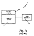
- the number of check bits required to implement the ECC depends on the number of data bits being read. As shown in Table 1, as a number of data bits being read increases, the number of required ECC bits also increases. Table 1 Data Bits ECC Bits 16 - 31 6 32-63 7 64 - 127 8 128 - 255 9
- An error correcting code circuit 10 includes a memory line 11, which is shown in Figure la including 30 data bits. Associated with the memory line 11 is an ECC cell 12. Referring to Table 1 above, six ECC bits are required to be stored in the ECC cell 12 to accomplish singlebit errorcornection and double bit error detection in the memory line 11. An ECC block 13 is used to generate the ECC bits and to perform the error correcting/detecting code operations including checking the data bits in the memory line 11 during read and write operations.
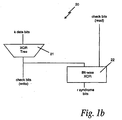
- Figure 1B is a block diagram of a portion of the ECC block 13 that generates check bits and syndrome bits.
- syndrome bits are the product of a comparison of the ECC bits originally stored with the data in the memory during a data store operation, and a new set of ECC bits generated based on the data that has been fetched from the memory such as would occur during execution of a read command, or any memory access, in a computer system. That is, a syndrome bit is simply the XOR of a corresponding received ECC bit with a newly generated ECC bit. If the combination of the retrieved and the newly generated ECC bits creates any non-zero syndrome bits, an error within the retrieved data has been detected.
- a circuit 20 includes an XOR tree 21 and a bit-wise XOR module 22.
- the ECC bits are generated simultaneously by processing the data bits using a parity check matrix, for example. Such generation of ECC bits is well known in the art.
- the syndrome bits are generated simultaneously from the data bits read according to standard decoding processes.
- the same XOR tree 21 may be used for both the ECC bits and the syndrome bits as shown in Figure 1B.
- an apparatus and a method subject the implementation of the ECC circuit to the various errors the ECC circuit is expected to correct/detect.
- the apparatus and the method verifies the ECC concept, the algorithm, and the implementation simultaneously.
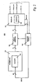
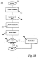
- FIG. 2 is a block diagram illustrating the apparatus and the method for verifying ECC.
- an apparatus 100 includes a transmitter 110 having an encoder 115.
- the transmitter 110 and the encoder 115 are coupled through an error injection circuit 120 to a receiver 130 having a decoder 135.
- a monitoring module 140 Also coupled to the encoder 115 and the decoder 135 is a monitoring module 140.
- the apparatus 100 may be implemented as an actual hardware device, or may be implemented as a simulation of a hardware device, using a hardware description language, such as VHDL or Verilog, for example, both of which are known in the art.
- the method and the apparatus 100 function to completely test the ECC by the coupling of the encoder 115 and the decoder 135 and then injecting possible errors.
- data are input to the encoder 115.
- the encoder 115 encodes the data to produce an output vector 112.
- the data input is 64 bits wide.
- the encoder will encode an additional 8 bits to the data input such that the output vector 112 is 72 bits wide.
- the output vector 112 is sent through error injection circuit 120, which introduces errors that the ECC is capable of correcting or detecting.
- the error injection circuit 120 also tests the ECC and its implementation by not introducing errors (a zero error case).
- the modified data are then fed directly to the decoder 135.
- the decoder 135 decodes the modified data and produces several output signals.
- the output signals may include a data out signal, a no error signal, a single error signal and a double (multiple) error signal.
- the decoder 135 may also provide an error_loc signal, which indicates a location of a bit in error.
- the error_loc signal may be similar to the syndrome mentioned above.
- Other output signals may also be provided.
- These output signals are provided to the monitoring module 140. The monitoring module 140 determines if the provided output signals are as expected. If the output signals are not as expected, then a problem may exist with the ECC or the ECC circuit.
- the apparatus 100 also checks for proper operation of the ECC in the presence of multiple errors.
- the error injection circuit 120 injects double errors (there are 2556 possibilities in this example).
- the apparatus 100 may be implemented in various ways, depending on the ECC verification methodology.
- the error injection circuit 120 may be implemented as an XOR of the data_out bits with a binary error vector of the same width as the data_out bits.
- the binary error vector may be randomly generated in a simulation environment for all the different error types. These error types include no error, single error and double error, for example.
- the binary error vector may also be hand coded and supplied to the error injection circuit 120.
- a formal verification module may include all error scenarios.
- the apparatus 100 may be used with any type of memory in a computer system.
- the ECC circuit 100 may be used with cache and with main memory.
- the apparatus may be used with any ECC. While the proceeding discussion described operation of the apparatus 100 with a SEC-DED. one of ordinary skill in the art would understand the method and the apparatus 100 may be used with ECCs that are capable of detecting and correcting multiple errors (e.g., DEC-TED codes).
- the apparatus 100 may be included on a dual in-line memory module (DIMM) card along with one or more memory chips and may be implemented within an ASIC chip, for example.
- the ASIC chip would serve to interconnect a data bus (not shown) of the computer system to the memory chips. Data passing from the data bus to the memory chips during execution ow a write operation would pass through the apparatus 100 prior to storage in the memory chips. Likewise, data passing from the memory chips to the data bus would also pass through the apparatus 100.
- the error detection and correction mechanism operates on the data as the data is being stored by the computer system in the memory chips.
- the data bus coupling the transmitter 110 and receiver 130 has sufficient bandwidth to carry all 72 bits in one clock cycle.
- the apparatus 100 may also be used with system busses having smaller bandwidths. In this case, multiple cycles may be needed to transmit all the data ad check bits.
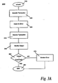
- Figures 3A and 3B illustrate processes that may be executed using the apparatus 100 shown in Figure 2.
- Figure 3A illustrates a process 200 when a no error signal is injected. The process begins with block 210.
- the encoder 115 encodes a transaction with an ECC. The transaction is then processed in error injection circuit 120, and a no error signal is injected, block 230.
- the transaction is decoded using the ECC.
- the monitor module 140 monitors the decoded transaction.
- Figure 3B illustrates a process 300 in which the error injection circuit 120 inserts a single-bit error.
Landscapes
- Physics & Mathematics (AREA)
- Probability & Statistics with Applications (AREA)
- Engineering & Computer Science (AREA)
- Theoretical Computer Science (AREA)
- Detection And Correction Of Errors (AREA)
- Techniques For Improving Reliability Of Storages (AREA)
- Error Detection And Correction (AREA)
- Detection And Prevention Of Errors In Transmission (AREA)
- For Increasing The Reliability Of Semiconductor Memories (AREA)
Applications Claiming Priority (2)
| Application Number | Priority Date | Filing Date | Title |
|---|---|---|---|
| US09/562,133 US6799287B1 (en) | 2000-05-01 | 2000-05-01 | Method and apparatus for verifying error correcting codes |
| US562133 | 2000-05-01 |
Publications (3)
| Publication Number | Publication Date |
|---|---|
| EP1160987A2 EP1160987A2 (en) | 2001-12-05 |
| EP1160987A3 EP1160987A3 (en) | 2003-04-09 |
| EP1160987B1 true EP1160987B1 (en) | 2006-02-08 |
Family
ID=24244934
Family Applications (1)
| Application Number | Title | Priority Date | Filing Date |
|---|---|---|---|
| EP01108612A Expired - Lifetime EP1160987B1 (en) | 2000-05-01 | 2001-04-05 | Method and apparatus for verifying error correcting codes |
Country Status (4)
| Country | Link |
|---|---|
| US (2) | US6799287B1 (enExample) |
| EP (1) | EP1160987B1 (enExample) |
| JP (1) | JP2001358702A (enExample) |
| DE (1) | DE60117066T2 (enExample) |
Cited By (1)
| Publication number | Priority date | Publication date | Assignee | Title |
|---|---|---|---|---|
| US9569582B2 (en) | 2014-01-03 | 2017-02-14 | International Business Machines Corporation | Template matching for resilience and security characteristics of sub-component chip designs |
Families Citing this family (53)
| Publication number | Priority date | Publication date | Assignee | Title |
|---|---|---|---|---|
| DK6488D0 (da) | 1988-01-07 | 1988-01-07 | Novo Industri As | Enzymer |
| FR2819603B1 (fr) * | 2001-01-16 | 2003-06-13 | Centre Nat Rech Scient | Procede d'injecteur d'erreurs par interruptions |
| US7389463B2 (en) * | 2001-05-29 | 2008-06-17 | Thomson Licensing | Hierarchical block coding for a packet-based communications system |
| US7051264B2 (en) * | 2001-11-14 | 2006-05-23 | Monolithic System Technology, Inc. | Error correcting memory and method of operating same |
| US7073117B1 (en) * | 2002-02-21 | 2006-07-04 | Ciena Corporation | Method and apparatus for generating bit errors in a forward error correction (FEC) system to estimate power dissipation characteristics of the system |
| MXPA04012474A (es) * | 2002-06-21 | 2005-09-20 | Thomson Licensing Sa | Metodo para correccion de error delantero. |
| US7401269B2 (en) * | 2003-05-10 | 2008-07-15 | Hewlett-Packard Development Company, L.P. | Systems and methods for scripting data errors to facilitate verification of error detection or correction code functionality |
| US7499674B2 (en) * | 2003-09-12 | 2009-03-03 | Nokia Corporation | Method and system for repeat request in hybrid ultra wideband-bluetooth radio |
| US7352998B2 (en) * | 2003-09-12 | 2008-04-01 | Nokia Corporation | Method and system for establishing a wireless communications link |
| US7782894B2 (en) * | 2003-09-12 | 2010-08-24 | Nokia Corporation | Ultra-wideband/low power communication having a dedicated removable memory module for fast data downloads—apparatus, systems and methods |
| US7702284B2 (en) | 2003-09-12 | 2010-04-20 | Arto Palin | Method and system for processing acknowledgments in a wireless communications network |
| US7278084B2 (en) * | 2003-10-29 | 2007-10-02 | Nokia Corporation | Method and system for providing communications security |
| US7697893B2 (en) * | 2004-06-18 | 2010-04-13 | Nokia Corporation | Techniques for ad-hoc mesh networking |
| US7392456B2 (en) * | 2004-11-23 | 2008-06-24 | Mosys, Inc. | Predictive error correction code generation facilitating high-speed byte-write in a semiconductor memory |
| US7779326B2 (en) * | 2005-03-01 | 2010-08-17 | The Texas A&M University System | Multi-source data encoding, transmission and decoding using Slepian-Wolf codes based on channel code partitioning |
| FR2883998A1 (fr) * | 2005-04-05 | 2006-10-06 | St Microelectronics Sa | Coprocesseur securise comprenant un circuit de detection d'un evenement |
| US7546514B2 (en) | 2005-04-11 | 2009-06-09 | Hewlett-Packard Development Company, L.P. | Chip correct and fault isolation in computer memory systems |
| US8181100B1 (en) * | 2008-02-07 | 2012-05-15 | Marvell International Ltd. | Memory fault injection |
| US8411662B1 (en) | 2005-10-04 | 2013-04-02 | Pico Mobile Networks, Inc. | Beacon based proximity services |
| DE102006001872B4 (de) * | 2006-01-13 | 2013-08-22 | Infineon Technologies Ag | Vorrichtung und Verfahren zum Überprüfen einer Fehlererkennungsfunktionalität einer Datenverarbeitungseinrichtung auf Angriffe |
| US7669095B2 (en) * | 2006-02-01 | 2010-02-23 | International Business Machines Corporation | Methods and apparatus for error injection |
| JP4946249B2 (ja) * | 2006-08-07 | 2012-06-06 | 富士通セミコンダクター株式会社 | Eccのコード長が変更可能な半導体メモリ装置 |
| EP1916534B1 (en) * | 2006-10-23 | 2009-12-16 | Onespin Solutions GmbH | Verification and generation of timing exceptions |
| KR100847560B1 (ko) * | 2006-12-11 | 2008-07-21 | 삼성전자주식회사 | 다운로드되는 펌웨어의 오류 정정을 위한 회로 및 방법 |
| DE102007028766A1 (de) * | 2007-06-22 | 2008-12-24 | Continental Teves Ag & Co. Ohg | Prüfverfahren und elektronische Schaltung zur sicheren seriellen Übertragung von Daten |
| US7827445B2 (en) * | 2007-12-19 | 2010-11-02 | International Business Machines Corporation | Fault injection in dynamic random access memory modules for performing built-in self-tests |
| US8627163B2 (en) * | 2008-03-25 | 2014-01-07 | Micron Technology, Inc. | Error-correction forced mode with M-sequence |
| US8413036B2 (en) * | 2008-11-28 | 2013-04-02 | Agere Systems Llc | Pseudorandom binary sequence checker with control circuitry for end-of-test check |
| US9380401B1 (en) | 2010-02-03 | 2016-06-28 | Marvell International Ltd. | Signaling schemes allowing discovery of network devices capable of operating in multiple network modes |
| US20110219266A1 (en) * | 2010-03-04 | 2011-09-08 | Qualcomm Incorporated | System and Method of Testing an Error Correction Module |
| EP2571172A4 (en) | 2010-05-11 | 2013-10-16 | Asip Solutions Inc | METHOD AND DEVICE FOR PROCESSING ERROR CORRECTION CODES |
| WO2012073071A1 (en) * | 2010-12-02 | 2012-06-07 | Freescale Semiconductor, Inc. | Error correcting device, method for monitoring an error correcting device and data processing system |
| CN102567132B (zh) * | 2011-12-30 | 2014-12-03 | 记忆科技(深圳)有限公司 | 端对端芯片数据通路保护装置及其方法 |
| US8806295B2 (en) * | 2012-05-24 | 2014-08-12 | International Business Machines Corporation | Mis-correction and no-correction rates for error control |
| US8918707B2 (en) | 2012-06-26 | 2014-12-23 | Freescale Semiconductor, Inc. | Codeword error injection via checkbit modification |
| JP6003735B2 (ja) * | 2013-03-18 | 2016-10-05 | 富士通株式会社 | Dimm擬似故障発生方法およびdimm擬似故障発生装置 |
| US10248521B2 (en) * | 2015-04-02 | 2019-04-02 | Microchip Technology Incorporated | Run time ECC error injection scheme for hardware validation |
| DE102015210651B4 (de) * | 2015-06-10 | 2022-10-27 | Infineon Technologies Ag | Schaltung und Verfahren zum Testen einer Fehlerkorrektur-Fähigkeit |
| KR102324769B1 (ko) * | 2015-06-29 | 2021-11-10 | 삼성전자주식회사 | 반도체 메모리 장치의 에러 정정 회로, 반도체 메모리 장치 및 이를 포함하는 메모리 시스템 |
| US10108512B2 (en) * | 2016-04-01 | 2018-10-23 | Intel Corporation | Validation of memory on-die error correction code |
| US10043588B2 (en) | 2016-12-15 | 2018-08-07 | SK Hynix Inc. | Memory device |
| KR20190043043A (ko) * | 2017-10-17 | 2019-04-25 | 에스케이하이닉스 주식회사 | 전자장치 |
| US11048602B2 (en) * | 2017-10-17 | 2021-06-29 | SK Hynix Inc. | Electronic devices |
| US10625752B2 (en) * | 2017-12-12 | 2020-04-21 | Qualcomm Incorporated | System and method for online functional testing for error-correcting code function |
| US10666294B2 (en) * | 2018-02-28 | 2020-05-26 | Hewlett Packard Enterprise Development Lp | Error correction code words with binomial bit error distribution |
| US10706950B1 (en) * | 2018-06-19 | 2020-07-07 | Cadence Design Systems, Inc. | Testing for memory error correction code logic |
| US11061771B2 (en) * | 2019-03-01 | 2021-07-13 | Micron Technology, Inc. | Extended error detection for a memory device |
| KR20220050315A (ko) | 2020-10-16 | 2022-04-25 | 삼성전자주식회사 | 반도체 메모리 장치 및 이를 포함하는 메모리 시스템 |
| CN112506730B (zh) * | 2020-11-10 | 2022-11-01 | 中国人民解放军战略支援部队信息工程大学 | 适用于网络交换芯片ecc功能验证的验证平台及验证方法 |
| US11209482B1 (en) * | 2020-11-30 | 2021-12-28 | Stmicroelectronics International N.V. | Methods and devices for testing comparators |
| KR20220127571A (ko) | 2021-03-11 | 2022-09-20 | 삼성전자주식회사 | 빌트-인-셀프-테스트 로직, 빌트-인-셀프 테스트 로직을 포함하는 메모리 장치, 및 메모리 모듈에 대한 테스트 방법 |
| CN114915380B (zh) * | 2022-07-19 | 2022-09-30 | 中国科学院宁波材料技术与工程研究所 | 基于can总线的低成本高实时自动纠错通讯系统及方法 |
| CN120029818B (zh) * | 2025-02-12 | 2025-10-24 | 上海芯钛信息科技有限公司 | 自动化提取与注错的ecc验证方法及装置 |
Citations (2)
| Publication number | Priority date | Publication date | Assignee | Title |
|---|---|---|---|---|
| JPS59200349A (ja) * | 1983-04-27 | 1984-11-13 | Nec Corp | 誤り訂正回路用診断回路 |
| US4561095A (en) * | 1982-07-19 | 1985-12-24 | Fairchild Camera & Instrument Corporation | High-speed error correcting random access memory system |
Family Cites Families (39)
| Publication number | Priority date | Publication date | Assignee | Title |
|---|---|---|---|---|
| US4794597A (en) * | 1986-03-28 | 1988-12-27 | Mitsubishi Denki Kabushiki Kaisha | Memory device equipped with a RAS circuit |
| US4759019A (en) * | 1986-07-10 | 1988-07-19 | International Business Machines Corporation | Programmable fault injection tool |
| JPH0212445A (ja) * | 1988-06-30 | 1990-01-17 | Mitsubishi Electric Corp | 記憶装置 |
| US5001712A (en) * | 1988-10-17 | 1991-03-19 | Unisys Corporation | Diagnostic error injection for a synchronous bus system |
| US4999837A (en) * | 1989-03-20 | 1991-03-12 | International Business Machines Corporation | Programmable channel error injection |
| JP2938999B2 (ja) * | 1991-05-23 | 1999-08-25 | 松下電器産業株式会社 | チューナ用半導体装置およびチューナ |
| US5502732A (en) * | 1993-09-20 | 1996-03-26 | International Business Machines Corporation | Method for testing ECC logic |
| US6545728B1 (en) * | 1994-05-04 | 2003-04-08 | Samsung Electronics Co., Ltd. | Digital television receivers that digitize final I-F signals resulting from triple-conversion |
| US5574855A (en) * | 1995-05-15 | 1996-11-12 | Emc Corporation | Method and apparatus for testing raid systems |
| WO1997050187A1 (en) * | 1996-06-27 | 1997-12-31 | Philips Electronics N.V. | Satellite receiver |
| US5812556A (en) * | 1996-07-03 | 1998-09-22 | General Signal Corporation | Fault tolerant switch fabric with control and data correction by hamming codes and error inducing check register |
| US5668816A (en) * | 1996-08-19 | 1997-09-16 | International Business Machines Corporation | Method and apparatus for injecting errors into an array built-in self-test |
| US6397357B1 (en) * | 1996-10-08 | 2002-05-28 | Dell Usa, L.P. | Method of testing detection and correction capabilities of ECC memory controller |
| US5958072A (en) * | 1997-01-13 | 1999-09-28 | Hewlett-Packard Company | Computer-system processor-to-memory-bus interface having repeating-test-event generation hardware |
| US6031878A (en) * | 1997-02-28 | 2000-02-29 | Maxim Integrated Products, Inc. | Direct-conversion tuner integrated circuit for direct broadcast satellite television |
| US5872790A (en) * | 1997-02-28 | 1999-02-16 | International Business Machines Corporation | ECC memory multi-bit error generator |
| US6356736B2 (en) * | 1997-02-28 | 2002-03-12 | Maxim Integrated Products, Inc. | Direct-conversion tuner integrated circuit for direct broadcast satellite television |
| US5875195A (en) * | 1997-03-31 | 1999-02-23 | International Business Machines Corporation | Method and apparatus for error injection techniques |
| US5901184A (en) * | 1997-06-18 | 1999-05-04 | Lsi Logic Corporation | Extended range voltage controlled oscillator for frequency synthesis in a satellite receiver |
| US6091931A (en) * | 1997-06-18 | 2000-07-18 | Lsi Logic Corporation | Frequency synthesis architecture in a satellite receiver |
| GB2328813B (en) * | 1997-08-28 | 2001-08-29 | Mitel Corp | A radio frequency zero IF direct down converter |
| US6218972B1 (en) * | 1997-09-11 | 2001-04-17 | Rockwell Science Center, Inc. | Tunable bandpass sigma-delta digital receiver |
| JPH11205172A (ja) * | 1998-01-12 | 1999-07-30 | Alps Electric Co Ltd | 衛星放送受信機用チュ−ナ |
| US5982823A (en) * | 1998-03-17 | 1999-11-09 | Northrop Grumman Corp | Direct frequency selection and down-conversion for digital receivers |
| US6182248B1 (en) * | 1998-04-07 | 2001-01-30 | International Business Machines Corporation | Method and tool for computer bus fault isolation and recovery design verification |
| US6134429A (en) * | 1998-04-10 | 2000-10-17 | Vlsi Technology, Inc. | Direct digital down conversion of a 10.8 MHz intermediate frequency signal in the personal handy phone system |
| US6067647A (en) * | 1998-09-02 | 2000-05-23 | Intel Corporation | Method and apparatus for inserting an error signal onto a bidirectional signal line |
| US6223309B1 (en) * | 1998-10-02 | 2001-04-24 | International Business Machines Corporation | Method and apparatus for ECC logic test |
| DE69920273T2 (de) * | 1998-11-12 | 2005-09-22 | Broadcom Corp., Irvine | Integrierte tunerarchitektur |
| US6237116B1 (en) * | 1998-11-16 | 2001-05-22 | Lockheed Martin Corporation | Testing error correcting code feature in computers that do not have direct hardware features for causing single bit and multi-bit errors |
| US6590929B1 (en) * | 1999-06-08 | 2003-07-08 | International Business Machines Corporation | Method and system for run-time logic verification of operations in digital systems |
| US6457147B1 (en) * | 1999-06-08 | 2002-09-24 | International Business Machines Corporation | Method and system for run-time logic verification of operations in digital systems in response to a plurality of parameters |
| US6618696B1 (en) * | 1999-06-14 | 2003-09-09 | The United States Of America As Represented By The National Security Agency | Method of testing and simulating communication equipment over multiple transmission channels |
| US6560725B1 (en) * | 1999-06-18 | 2003-05-06 | Madrone Solutions, Inc. | Method for apparatus for tracking errors in a memory system |
| US6473871B1 (en) * | 1999-08-31 | 2002-10-29 | Sun Microsystems, Inc. | Method and apparatus for HASS testing of busses under programmable control |
| US6539503B1 (en) * | 1999-11-23 | 2003-03-25 | Hewlett-Packard Company | Method and apparatus for testing error detection |
| US6892336B1 (en) * | 2000-03-17 | 2005-05-10 | Applied Micro Circuits Corporation | Gigabit ethernet performance monitoring |
| CA2357491A1 (en) * | 2001-09-17 | 2003-03-17 | Ralph Mason | Filter tuning using direct digital sub-sampling |
| US6512472B1 (en) * | 2002-01-15 | 2003-01-28 | Motorola, Inc. | Method and apparatus for optimizing dynamic range of a wideband analog-to-digital converter |
-
2000
- 2000-05-01 US US09/562,133 patent/US6799287B1/en not_active Expired - Lifetime
-
2001
- 2001-04-05 DE DE60117066T patent/DE60117066T2/de not_active Expired - Fee Related
- 2001-04-05 EP EP01108612A patent/EP1160987B1/en not_active Expired - Lifetime
- 2001-04-17 JP JP2001117596A patent/JP2001358702A/ja active Pending
-
2004
- 2004-06-16 US US10/867,769 patent/US20040243887A1/en not_active Abandoned
Patent Citations (2)
| Publication number | Priority date | Publication date | Assignee | Title |
|---|---|---|---|---|
| US4561095A (en) * | 1982-07-19 | 1985-12-24 | Fairchild Camera & Instrument Corporation | High-speed error correcting random access memory system |
| JPS59200349A (ja) * | 1983-04-27 | 1984-11-13 | Nec Corp | 誤り訂正回路用診断回路 |
Non-Patent Citations (4)
| Title |
|---|
| "INTERNET CITATION", Retrieved from the Internet <URL:http://www.eccpage.com/new_rs_erasures.c> [retrieved on 20040729] * |
| ANONYMOUS: "Verifying parity checkers/generators", RESEARCH DISCLOSURE, KENNETH MASON PUBLICATIONS, vol. 285, no. 10, January 1988 (1988-01-01), HAMPSHIRE, GB * |
| PATENT ABSTRACTS OF JAPAN vol. 009, no. 064 (P - 343) 23 March 1985 (1985-03-23) * |
| YÜCEL M.D.: "Implementation of a real time Reed-Solomon Encoder using TMS32010", IEEE PACIFIC RIM CONFERENCE ON COMMUNICATIONS, COMPUTERS AND SIGNAL PROCESSING, 2 July 1989 (1989-07-02), pages 341 - 344 * |
Cited By (1)
| Publication number | Priority date | Publication date | Assignee | Title |
|---|---|---|---|---|
| US9569582B2 (en) | 2014-01-03 | 2017-02-14 | International Business Machines Corporation | Template matching for resilience and security characteristics of sub-component chip designs |
Also Published As
| Publication number | Publication date |
|---|---|
| EP1160987A2 (en) | 2001-12-05 |
| US6799287B1 (en) | 2004-09-28 |
| JP2001358702A (ja) | 2001-12-26 |
| US20040243887A1 (en) | 2004-12-02 |
| DE60117066D1 (de) | 2006-04-20 |
| EP1160987A3 (en) | 2003-04-09 |
| DE60117066T2 (de) | 2006-08-24 |
Similar Documents
| Publication | Publication Date | Title |
|---|---|---|
| EP1160987B1 (en) | Method and apparatus for verifying error correcting codes | |
| US7900100B2 (en) | Uncorrectable error detection utilizing complementary test patterns | |
| US7797609B2 (en) | Apparatus and method for merging data blocks with error correction code protection | |
| US7149947B1 (en) | Method of and system for validating an error correction code and parity information associated with a data word | |
| US6009548A (en) | Error correcting code retrofit method and apparatus for multiple memory configurations | |
| JP3325914B2 (ja) | データ用誤り訂正検出方法及びコンピュータ・メモリ用 誤り検出回路 | |
| JP4071940B2 (ja) | メモリ設計のための共有式誤り訂正 | |
| US4817095A (en) | Byte write error code method and apparatus | |
| EP0186719B1 (en) | Device for correcting errors in memories | |
| US5384788A (en) | Apparatus and method for optimal error correcting code to parity conversion | |
| US6301680B1 (en) | Technique for correcting single-bit errors and detecting paired double-bit errors | |
| US4740968A (en) | ECC circuit failure detector/quick word verifier | |
| US7587658B1 (en) | ECC encoding for uncorrectable errors | |
| EP0188192A2 (en) | Extended error correction for package error correction codes | |
| US11126500B2 (en) | Error detection and correction with integrity checking | |
| JPS6061837A (ja) | エラ−訂正装置 | |
| US20130346798A1 (en) | Codeword error injection via checkbit modification | |
| EP1206739A1 (en) | Methods and apparatus for correcting soft errors in digital data | |
| JPS6349245B2 (enExample) | ||
| US6393597B1 (en) | Mechanism for decoding linearly-shifted codes to facilitate correction of bit errors due to component failures | |
| US10860415B2 (en) | Memory architecture including response manager for error correction circuit | |
| Asuvaran et al. | Low delay error correction codes to correct stuck-at defects and soft errors | |
| CN106531224A (zh) | 一种基于sram型fpga的ram数据可靠性加固装置及方法 | |
| US11069421B1 (en) | Circuitry for checking operation of error correction code (ECC) circuitry | |
| CN109753369A (zh) | 一种寄存器及内存中顺序数组的数据编码及校验方法 |
Legal Events
| Date | Code | Title | Description |
|---|---|---|---|
| PUAI | Public reference made under article 153(3) epc to a published international application that has entered the european phase |
Free format text: ORIGINAL CODE: 0009012 |
|
| AK | Designated contracting states |
Kind code of ref document: A2 Designated state(s): AT BE CH CY DE DK ES FI FR GB GR IE IT LI LU MC NL PT SE TR |
|
| AX | Request for extension of the european patent |
Free format text: AL;LT;LV;MK;RO;SI |
|
| PUAL | Search report despatched |
Free format text: ORIGINAL CODE: 0009013 |
|
| AK | Designated contracting states |
Kind code of ref document: A3 Designated state(s): AT BE CH CY DE DK ES FI FR GB GR IE IT LI LU MC NL PT SE TR |
|
| AX | Request for extension of the european patent |
Extension state: AL LT LV MK RO SI |
|
| 17P | Request for examination filed |
Effective date: 20030918 |
|
| AKX | Designation fees paid |
Designated state(s): DE FR GB |
|
| 17Q | First examination report despatched |
Effective date: 20040119 |
|
| GRAP | Despatch of communication of intention to grant a patent |
Free format text: ORIGINAL CODE: EPIDOSNIGR1 |
|
| GRAS | Grant fee paid |
Free format text: ORIGINAL CODE: EPIDOSNIGR3 |
|
| GRAA | (expected) grant |
Free format text: ORIGINAL CODE: 0009210 |
|
| AK | Designated contracting states |
Kind code of ref document: B1 Designated state(s): DE FR GB |
|
| REG | Reference to a national code |
Ref country code: GB Ref legal event code: FG4D |
|
| REF | Corresponds to: |
Ref document number: 60117066 Country of ref document: DE Date of ref document: 20060420 Kind code of ref document: P |
|
| PG25 | Lapsed in a contracting state [announced via postgrant information from national office to epo] |
Ref country code: GB Free format text: LAPSE BECAUSE OF NON-PAYMENT OF DUE FEES Effective date: 20060508 |
|
| PG25 | Lapsed in a contracting state [announced via postgrant information from national office to epo] |
Ref country code: DE Free format text: LAPSE BECAUSE OF NON-PAYMENT OF DUE FEES Effective date: 20061101 |
|
| PLBE | No opposition filed within time limit |
Free format text: ORIGINAL CODE: 0009261 |
|
| STAA | Information on the status of an ep patent application or granted ep patent |
Free format text: STATUS: NO OPPOSITION FILED WITHIN TIME LIMIT |
|
| 26N | No opposition filed |
Effective date: 20061109 |
|
| GBPC | Gb: european patent ceased through non-payment of renewal fee |
Effective date: 20060508 |
|
| EN | Fr: translation not filed | ||
| PG25 | Lapsed in a contracting state [announced via postgrant information from national office to epo] |
Ref country code: FR Free format text: LAPSE BECAUSE OF FAILURE TO SUBMIT A TRANSLATION OF THE DESCRIPTION OR TO PAY THE FEE WITHIN THE PRESCRIBED TIME-LIMIT Effective date: 20070330 |
|
| PG25 | Lapsed in a contracting state [announced via postgrant information from national office to epo] |
Ref country code: FR Free format text: LAPSE BECAUSE OF FAILURE TO SUBMIT A TRANSLATION OF THE DESCRIPTION OR TO PAY THE FEE WITHIN THE PRESCRIBED TIME-LIMIT Effective date: 20060430 |
|
| PG25 | Lapsed in a contracting state [announced via postgrant information from national office to epo] |
Ref country code: FR Free format text: LAPSE BECAUSE OF FAILURE TO SUBMIT A TRANSLATION OF THE DESCRIPTION OR TO PAY THE FEE WITHIN THE PRESCRIBED TIME-LIMIT Effective date: 20060208 |