TECHNICAL FIELD OF THE INVENTION
The present invention relates to a surface acoustic wave device
for use in wireless communications equipment and the like and method
of manufacture thereof.
BACKGROUND OF THE TECHNOLOGY
Fig. 23 is a cross-sectional view of a conventional surface
acoustic wave device (hereinafter SAW device). Referring to Fig.
23, a description will be given below on the method of manufacture
of the conventional SAW device.
First, interdigital transducer electrodes (IDT electrodes)
101 and connection electrodes 102 are formed by forming vacuum
deposited aluminum film on a disk (wafer) of piezoelectric material
followed by exposing with a pattern of predetermined configuration
and developing. Subsequently, acoustic absorbers 103 are formed by
coating a silicone resin on both sides of the IDT electrodes 101 by
screen printing and heat treatment. In this way, a number of surface
acoustic wave elements 105 (SAW elements) are collectively formed
on the wafer. Subsequently, the wafer is diced into individual SAW
elements 105.
Next, a SAW element 105 is secured with adhesive 108 in a package
107 having external terminals 106, and the external terminals 106
and connection electrodes 102 are electrically connected with thin
metal wires 109. Subsequently, opening of the package 107 is sealed
with a lid 110.
When the acoustic absorbers 103 are formed by screen printing
in this manner, the dimensional accuracy is poor and also their cross
sections become dome-like due to drips caused by flow of the resin,
thus suffering from the upper surfaces becoming curved and difficulty
in forming with a uniform height.
Furthermore, when mounting the SAW element 105 in the package
107, as the SAW element 105 is transferred by sucking its surface
with a vacuum chuck, there is a difficulty in sucking because the
top surfaces of the acoustic absorbers 103 are curved and their
heights are different. In addition, piezoelectric substrate 100 may
incline relative to the bottom surface of the package 107 thus
presenting a possibility of causing mounting failure.
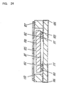
Fig. 24 is a cross-sectional view of another conventional SAW
device. While thin metal wires 109 connect the connection electrodes
102 and the external terminals 106 in the conventional SAW device
of Fig. 23, in another conventional SAW device shown in Fig. 24,
projecting electrodes 111 (bumps) make the connection.
In this case, too, there is a possibility of causing connection
failure when the heights of the acoustic absorbers 103 are non-uniform
and are greater than the bumps 111.
DISCLOSURE OF THE INVENTION
The present invention addresses the above issues and aims at
providing a SAW device that can prevent mounting failure when mounting
a SAW element in a package.
In order to attain this object, the SAW device of the present
invention comprises a package having an external terminal, a SAW
element housed in the package, and a lid for sealing opening of the
package, wherein the SAW element further comprises on the surface
of a piezoelectric substrate at least an IDT electrode, a connection
electrode electrically connected to the IDT electrode, and an
acoustic absorber formed on the outside of the IDT electrode, that
is, on an end portion of the piezoelectric substrate, in a manner
such that its top surface is parallel to the main surface of the
piezoelectric substrate. As the surface of the acoustic absorber
is parallel to the main surface of the piezoelectric substrate in
this way, and as the top surface of the acoustic absorber is a plane,
it is easy to suck the SAW element with a vacuum chuck when mounting
in a package and it is possible to securely mount it at a predetermined
position of the package.
BRIEF DESCRIPTION OF THE DRAWINGS
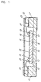
Fig. 1 is a cross-sectional view of a SAW device in a first
exemplary embodiment of the present invention. Fig. 2 is a top view
of the SAW device before sealing with a lid in the first exemplary
embodiment of the present invention. Fig. 3 is a cross-sectional
view to illustrate manufacturing process of the SAW device in the
first exemplary embodiment of the present invention.
Fig. 4 is a top view of a SAW device before sealing with a lid
in a second exemplary embodiment of the present invention. Fig. 5
is a cross-sectional view of the SAW device in the second exemplary
embodiment of the present invention.
Fig. 6 is a cross-sectional view of a SAW device in a third
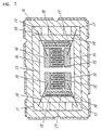
exemplary embodiment of the present invention. Fig. 7 is a top view
of the SAW device before sealing with a lid in the third exemplary
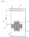
embodiment of the present invention. Fig. 8 is an illustrative
diagram of the manufacturing process of the SAW device in the third
exemplary embodiment of the present invention.
Fig. 9 is a top view of a SAW element in a fourth exemplary
embodiment of the present invention. Fig. 10 is a cross-sectional
view of a SAW device in the fourth exemplary embodiment of the present
invention. Fig. 11 is a cross-sectional view of a SAW device in the
fourth exemplary embodiment of the present invention.
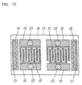
Fig. 12 is a top view of a SAW element in a fifth exemplary
embodiment of the present invention. Fig. 13 is a cross-sectional
view of a SAW device in the fifth exemplary embodiment of the present
invention.
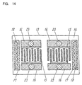
Fig. 14 is a top view of a SAW element in a sixth exemplary
embodiment of the present invention. Fig. 15 is a cross-sectional
view of a SAW device in the sixth exemplary embodiment of the present
invention.
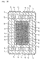
Fig. 16 is a top view of a SAW element in a seventh exemplary
embodiment of the present invention. Fig. 17 is a cross-sectional
view of a SAW device in the seventh exemplary embodiment of the present
invention.
Fig. 18 is a cross-sectional view of a SAW device in an eighth
exemplary embodiment of the present invention.
Fig. 19 is a top view of a SAW device before sealing with a
lid in a ninth exemplary embodiment of the present invention.
Fig. 20 is a top view of a SAW device before sealing with a
lid in a tenth exemplary embodiment of the present invention.
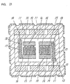
Fig. 21 is a top view of a SAW device before sealing with a
lid in an eleventh exemplary embodiment of the present invention.
Fig. 22 is a cross-sectional view of a SAW device in a twelfth
exemplary embodiment of the present invention.
Fig. 23 is a cross-sectional view of a conventional SAW device.
Fig. 24 is a cross-sectional view of a conventional SAW device.
DESCRIPTION OF THE PREFERRED EMBODIMENTS
Referring to drawings, a description will be given below on
exemplary embodiments of the SAW device and method of manufacture
thereof of the present invention.
First Exemplary Embodiment:
Referring to Figs. 1 to 3, a description will be given on a
first exemplary embodiment of the present invention.
A uniform thickness vapor deposited film composed of aluminum
or a metal having aluminum as the main constituent is formed on the
main surface of a wafer composed of a piezoelectric material such
as quartz, LiTaO3, LiNbO3, and the like. Positive type photoresist
is then uniformly coated by spin coating on top of the vapor deposited
film. Next, the photoresist is exposed and developed so as to make
IDT electrodes 15 having a desired shape, connection electrodes 16
to be connected to the IDT electrodes 15, and underlying metal layers
17 to be disposed at the locations where acoustic absorbers are to
be formed, and then the vapor deposited film is etched to obtain IDT
electrodes 15, connection electrodes 16, and underlying metal layers
17, and the photoresist is removed. Here, the underlying metal layers
17 are formed to a size greater than the acoustic absorbers to be
formed.
Subsequently, the entire main surface of the wafer whereon the
IDT electrodes 15 have been formed is covered with a negative
photoresist film, which is then pressed while being heated. The
exposed portion of the film resist is to become acoustic absorbers
18 and a film resist having the same thickness as that of the acoustic
absorbers 18 are used.
Subsequently, acoustic absorbers 18 are formed by exposing and
developing the portion which will form the acoustic absorbers 18 in
a manner such that the film resist of that portion will remain. After
development, moisture in the acoustic absorbers 18 is removed so as
to improve adhesion with the piezoelectric substrate 14. When
moisture is remaining in the acoustic absorbers 18, there is a
possibility of causing a change in the quality of the acoustic
absorbers 18 or corrosion of the IDT electrodes 15. A plurality of
SAW elements 13 are formed on the wafer in this manner.
Next, the wafer is cut into individual SAW elements 13 with
a dicer while spraying with water. After removing moisture, a SAW
element 13 is transferred by sucking its surface, that is, the
surfaces of the acoustic absorbers 18 with a vacuum chuck 30 shown
in Fig. 3, and is mounted in a package 10 coated with an adhesive
12. During this process, as the acoustic absorbers 18 have the same
thickness and, in addition, as their top surfaces are formed parallel
to the surface of the substrate 14, the SAW element 13 can be securely
sucked with the vacuum chuck 30 and can be accurately mounted in the
package 10.
Next, as illustrated in Fig. 2, the connection electrodes 16
of the SAW element 13 and the external terminals 11 of the package
10 are electrically connected with thin metal wires 19, the opening
of the package 10 is sealed with a lid 20, and a SAW device shown
in Fig. 1 is obtained.
Second Exemplary Embodiment:
Referring to Figs. 4 and 5, a description will be given on a
second exemplary embodiment of the present invention.
First, a plurality of SAW elements 13 having IDT electrodes
15, connection electrodes 16, and underlying metal layers 17 are
formed on a wafer in a manner similar to the first exemplary embodiment.
Next, a coupling layer 21 is formed by uniformly spin coating a
silane-based underlying coupling agent over the entire surface on
the side of the wafer where the IDT electrodes 15 have been formed.
Subsequently, solvent component in the coupling layer 21 is removed
by drying.
Afterwards, as in the first exemplary embodiment, the entire
main surface of the wafer is covered with a negative photoresist film,
which is then pressed while being heated. As the film resist, one
having the same thickness as the thickness of the acoustic absorbers
18 to be formed is used. Next, that portion of the film resist which
will form the acoustic absorber 18 is exposed and developed. After
acoustic absorbers 18 have been formed, moisture in the acoustic
absorbers 18 is removed. Next, after dicing the wafer into individual
SAW elements 13 as in the first exemplary embodiment, a SAW element
13 is mounted in a package 10 and a SAW device as illustrated in Figs.
4 and 5 is obtained.
In this exemplary embodiment, too, as in the first exemplary
embodiment, the top surfaces of the acoustic absorbers 18 are formed
parallel to the surface of the piezoelectric substrate 14 thus
enabling secure suction of the SAW element 13 with the vacuum chuck
30 shown in Fig. 3 and mounting in the package 10.
Furthermore, as the silane-based coupling layer 21 formed in
this exemplary embodiment has a large force of adhesion with the
acoustic absorbers 18 and the piezoelectric substrate 14, and is
extremely thin as it is a monomolecular layer, it enables to greatly
enhance the adhesion strength between the acoustic absorbers 18 and
the piezoelectric substrate 14 without affecting the sound absorbing
effect. As a result, when dicing the wafer on which a plurality of
SAW elements 13 have been formed into individual SAW elements 13,
peeling off the acoustic absorbers 18 from the piezoelectric
substrate 14 due to sprayed water can be prevented. In addition,
acoustic absorbers 18 that are stronger to thermal stress and the
like to be experienced while sealing opening of the package 10 with
a lid 20 with solder, for example, or mounting a SAW device onto a
circuit board by solder reflow method can be formed.
In the meantime, although only necessary parts of the coupling
layer 21 are shown in Figs. 4 and 5 for easy understanding, in this
second exemplary embodiment, the coupling layer 21 is provided over
the entire surface of the piezoelectric substrate 14 covering the
IDT electrodes 15 and the connection electrodes 16.
Third Exemplary Embodiment:
Referring to Figs. 6, 7, and 8, a description will be given
on a third exemplary embodiment of the present invention.
IDT electrodes 15, connection electrodes 16, and underlying
metal layers 17 composed of aluminum film or aluminum alloy film are
first formed on a wafer by photolithography in a manner similar to
the first exemplary embodiment. Next, as illustrated in Fig. 8, a
wafer 81 on which SAW elements 13 have been formed and an electrode
85 made of stainless steel and the like are immersed in a liquid
electrolyte 83, and a voltage is applied or a current is supplied
from a power supply 86 using the electrode 85 as the cathode and a
current supplying wire 87 that collects leads 82 form the IDT
electrodes 15, connection electrodes 16 and the underlying metal
layers 17 as the anode. Here, the numeral 84 is a chemically resistant
vessel. With this treatment, surfaces of the IDT electrodes 15,
connection electrodes 16 and the metal layers 17 including respective
sides are oxidized and are covered with a protective film 22 as shown
in Fig. 6. Then, the wafer 81 is pulled out from the liquid
electrolyte 83 and cleansed by dipping in pure water.
Next, the wafer 81 is diced into individual SAW elements 13
after forming a coupling layer 21 and acoustic absorbers 18 in a manner
similar to the second exemplary embodiment.
Next, a SAW element 13 is mounted in a manner similar to the
second exemplary embodiment in a package 10 coated with an adhesive
12, external terminals 11 and connection electrodes 16 are
electrically connected with thin metal wires 19 as illustrated in
Fig. 7, opening of the package 10 is sealed with a lid 20, and a SAW
device shown in Fig. 6 is obtained.
In this exemplary embodiment, too, as in the first exemplary
embodiment, the top surfaces of the acoustic absorbers 18 are formed
parallel to the main surface of the piezoelectric substrate 14 thus
enabling secure suction of the SAW element 13 with the vacuum chuck
30 shown in Fig. 3 and mounting in the package 10.
Furthermore, in this exemplary embodiment, too, the
silane-based coupling layer 21 can greatly enhance the adhesion
strength between the acoustic absorbers 18 and the piezoelectric
substrate 14 without affecting the sound absorbing effect. As a
result, peeling off the acoustic absorbers 18 from the piezoelectric
substrate 14 when dicing the wafer into individual SAW elements 13
by spraying water can be prevented. In addition, acoustic absorbers
18 that are stronger to thermal stress and the like to be experienced
when solder sealing an opening of the package 10 with a lid 20, for
example, or mounting a SAW device on a circuit board by reflow and
other methods can be obtained.
In this exemplary embodiment, anodic oxidation was carried out
after forming the IDT electrodes 15 and connection electrodes 16.
As the developing solution for photosensitive resin is generally
alkaline, there is a possibility of the IDT electrodes 15 and
connection electrodes 16 that consist of aluminum or a metal having
aluminum as the main constituent being eroded when developing the
film resist that will form the acoustic absorbers 18. However, by
covering the surfaces including the sides of the IDT electrodes 15
and the connection electrodes 16 with a protective film 22 consisting
of alkali resistant aluminum oxide as in this exemplary embodiment,
each of the electrodes can be protected against adverse effect by
the developing solution.
Also, as the protective film 22 is electrically insulating,
short-circuit failure of electrodes can be prevented in the event
an electrically conductive foreign object drops onto the SAW element
13.
In this exemplary embodiment, anodic oxidation was carried out
after the IDT electrodes 15, connection electrodes 16 and underlying
metal layers 17 had been formed; however, it does not matter if anodic
oxidation of the surface of vapor deposited film having aluminum or
aluminum alloy as the main constituent is carried out before forming
the IDT electrodes 15, connection electrodes 16, and underlying metal
layers 17, followed by formation of the IDT electrodes 15, the
connection electrodes 16, and the underlying metal layers 17 thereby
making their top surfaces covered with an insulating protective film.
In this case, during the period of development for forming the IDT
electrodes 15, the connection electrodes16, and the underlying metal
layers 17, at least surfaces of the IDT electrodes 15 and the
connection electrodes 16 will not be eroded by alkaline developing
solution. However, as the sides are not covered with the protective
film 22, it is preferable to carry out anodic oxidation after forming
the IDT electrodes 15 as in the above-mentioned exemplary embodiment
in order to prevent erosion by the developing solution for forming
the acoustic absorbers 18.
By carrying out anodic oxidation and covering the surface with
a protective film 22 either before or after forming the IDT electrodes
15 in this way, an effect of preventing erosion of the IDT electrodes
15 and the connection electrodes 16 due to alkaline developing
solution higher than by not forming a protective film 22 can be
obtained.
Fourth Exemplary Embodiment:
Referring to Figs. 9, 10, and 11, a description will be given
on a fourth exemplary embodiment of the present invention.
First, IDT electrodes 15, connection electrodes 16, and
underlying metal layers 17 are formed on a wafer in a manner similar
to the first exemplary embodiment followed by forming acoustic
absorbers 18 on the underlying metal layers 17. The acoustic
absorbers 18 have a height enough for forming a space necessary for
the IDT electrodes 15 to excite surface acoustic waves (SAW) after
being packaged in a package 10.
Next, gold bumps 23 are formed on the connection electrodes
16. The height of the bumps 23 is made higher than that of the acoustic
absorbers 18.
Subsequently, the wafer is diced in the same way as in the first
exemplary embodiment to obtain a SAW element 13 illustrated in Fig.
9.
The SAW element 13 is then mounted with the side having the
bumps 23 facedown in the package 10 having external terminals 11,
and the connection electrodes 16 of the SAW element 13 and the external
terminals 11 are electrically connected through the bumps 23.
During this process, the height of the bumps 23 decreases due
to heating and pressing.
In the case of conventional acoustic absorbers 103 shown in
Fig. 24, as the height of each of the acoustic absorbers 103 differs
and its cross section is domed, in connecting connection electrodes
102 of a SAW element 105 and external terminals 106 of a package 107
using bumps 111, there is a possibility of not being able to obtain
a SAW device having desired characteristic since the SAW element 105
cannot be horizontally mounted in the package 107 when the height
of bumps 111 has decreased to its minimum,.
However, in this exemplary embodiment, as the heights of the
acoustic absorbers 18 are fixed and their top surfaces are parallel
to the piezoelectric substrate 14, in the event the height of bumps
23 has lowered as shown in Fig. 11 during the mounting process, the
acoustic absorbers 18 work as stoppers and prevent the bumps 23 from
becoming lower than the height of the acoustic absorbers 18 thereby
enabling to secure enough space for the IDT electrodes 15 to excite
SAW. Also, as the SAW element 13 can be horizontally mounted, the
dispersion of joining strength between the bumps 23 and the connection
electrodes 16 can be reduced. In other words, a SAW element 13 such
as this is strong against mechanical and thermal stress.
Thereafter, opening of the package 10 is sealed with a lid 20
to obtain a SAW device as illustrated in Fig. 10.
While bumps 23 are formed with gold in this exemplary
embodiment, they may be formed with solder and the like.
Fifth Exemplary Embodiment:
Referring to Figs. 12 and 13, a description will be given on
a fifth exemplary embodiment of the present invention.
First, IDT electrodes 15, connection electrodes 16, underlying
metal layers 17, and coupling layers 21 are formed on a wafer in a
manner similar to the second exemplary embodiment.
Next, the entire surface of the wafer is covered with a negative
photosensitive film resist and heated, and the film resist is pressed.
As the film resist, one having the same thickness as that of the
acoustic absorbers 18 to be formed is used. Next, the film resist
is exposed and developed in a manner such that the portion of the
film resist forming the acoustic absorbers 18 will remain and the
acoustic absorbers 18 are obtained. The acoustic absorbers 18 have
a height enough for the IDT electrodes 15 to form a space necessary
for exciting SAW after being mounted in a package 10.
Next, the wafer is diced into individual SAW elements 13 as
shown in Fig. 12 after forming bumps 23 on the connection electrodes
16 in a manner similar to the fourth exemplary embodiment, mounted
in a package 10, and a SAW device as shown in Fig. 13 is obtained.
In this exemplary embodiment, too, as in the fourth exemplary
embodiment, as the acoustic absorbers 18 work as stoppers at the time
the SAW element 13 is being mounted, the height of the bumps 23 will
not become lower than the height of the acoustic absorbers 18 and
a space necessary for the IDT electrodes 15 to excite SAW can be secured.
Also, during this process, as the SAW element 13 can be horizontally
mounted, the dispersion of adhesion strength between the bumps 23
and the connection electrodes 16 can be reduced. In other words,
a SAW device such as this is strong against mechanical and thermal
stress.
Furthermore, in this exemplary embodiment, as in the second
exemplary embodiment, by forming a coupling layer 21 between the
underlying metal layers 17 and the acoustic absorbers 18, the adhesion
strength between the acoustic absorbers 18 and the piezoelectric
substrate 14 can be greatly enhanced without affecting the sound
absorbing effect. As a result, peeling off the acoustic absorbers
18 from the piezoelectric substrate 14 by spraying water when dicing
the wafer into individual SAW elements 13 can be prevented. In
addition, acoustic absorbers 18 that are stronger to stress such as
thermal stress to be experienced while solder sealing opening of the
package 10 with a lid 20, for example, or mounting a SAW device on
a circuit board by reflow and other methods can be provided.
Although only necessary parts of the coupling layer 21 are
shown in Figs. 12 and 13 for ease of understanding, in this exemplary
embodiment the coupling layer 21 is provided over the entire surface
of the piezoelectric substrate 14 covering the IDT electrodes 15 and
the connection electrodes 16.
Sixth Exemplary Embodiment:
Referring to Figs. 14 and 15, a description will be given on
a sixth exemplary embodiment of the present invention.
First, IDT electrodes 15, connection electrodes 16, and
underlying metal layers 17 of which the surfaces and the sides have
been covered with an insulating protective film 22 are formed in a
manner similar to the third exemplary embodiment.
Going through the same subsequent processes as in the fourth
and fifth exemplary embodiments, acoustic absorbers 18 are formed
on the underlying metal layers 17. After further forming bumps 23
on the connection electrodes 16, wafer is diced into individual SAW
elements 13 shown in Fig. 14. Next, a SAW device as shown in Fig.
15 is fabricated by mounting a SAW element 13 in a package 10 and
sealing with a lid 20.
In this exemplary embodiment, as in the third exemplary
embodiment, since the surfaces and sides of the IDT electrodes 15,
connection electrodes 16, and underlying metal layers 17 are covered
with a protective film 22, erosion of the IDT electrodes 15 and the
connection electrodes 16 by alkaline liquid electrolyte during
development for the formation of the acoustic absorbers 18 can be
preventented.
Also, as described in the third exemplary embodiment, the
electrically insulating protective film 22 may be formed on the
surfaces of the IDT electrodes 15 and the connection electrodes 16
by carrying out anodic oxidation after a metal film of aluminum or
aluminum alloy has been formed on the wafer prior to the formation
of the IDT electrodes 15, connection electrodes 16, and underlying
metal layers 17.
Seventh Exemplary Embodiment:
Referring to Figs. 16 and 17, a description will be given on
a seventh exemplary embodiment of the present invention. In this
exemplary embodiment, only the difference from the SAW device of the
fourth exemplary embodiment will be described.
In this exemplary embodiment, as shown in Fig. 16, underlying
metal layers 17 and acoustic absorber 18 to be formed thereon are
formed in the shape of a frame on the periphery of a piezoelectric
substrate 14 in a manner such that they surround IDT electrodes 15
and connection electrodes 16. The method of formation is the same
as in the fourth exemplary embodiment.
After a SAW element 13 has been mounted in a package 10, a filler
25 composed of a silicone-based resin is filled between the SAW
element 13 and the inner wall of the package 10 and then cured by
heating. During this process, the frame-shaped acoustic absorber
18 prevents the filler 25 from flowing into the SAW excitation space
of the IDT electrodes 15.
In addition, the filler 25 has, after being cured, a higher
elasticity than the acoustic absorber 18 and can absorb spurious waves
that have not been absorbed by the acoustic absorber 18 and can also
relieve the stress applied to the SAW element 13 due to the difference
in thermal expansion coefficients between those of the SAW element
13 and the package 10 thus preventing change of characteristics.
Eighth Exemplary Embodiment:
Referring to Fig. 18, a description will be given on an eighth
exemplary embodiment of the present invention.
The difference of a SAW device of this exemplary embodiment
from the SAW device of the seventh exemplary embodiment lies in that
a filler 25 is provided not only between the SAW element 13 and the
inner wall of the package 10 but also on the rear surface of the SAW
element 13 facing a lid 20. Other structure is the same. As a result,
a further higher effect of absorbing spurious waves is obtained
compared with that of the SAW device of the seventh exemplary
embodiment.
While the filler 25 is provided in this exemplary embodiment
over the entire rear surface of the SAW element 13 facing the lid
20, similar effect of absorbing spurious waves is obtainable by
providing only on the portions corresponding to the IDT electrodes
15.
Also, when sealing the package 10 with the lid 20, it is
preferable that care be taken not to make the filler 25 provided on
the rear surface of the SAW element 13 facing the lid 20 and the lid
20 come in contact with each other in order to prevent deterioration
of the characteristics caused by deformation of the SAW element 13
due to an excessive pressure applied from the rear surface of the
SAW element 13.
Ninth Exemplary Embodiment:
Referring to Fig. 19, a description will be given on a ninth
exemplary embodiment of the present invention.
In this exemplary embodiment, as illustrated in Fig. 19, two
pairs of IDT electrodes 15 are integrated into one unit, two surface
acoustic wave units (SAW units) 27 provided with reflector electrodes
26 on both sides of them are provided in parallel on a piezoelectric
substrate 14, and an acoustic absorber 18 is formed on the
piezoelectric substrate 14 between the SAW units 27 with intervention
of an underlying metal layer 17. By employing this structure,
acoustic coupling between the two SAW units 27 can be suppressed,
providing a superior quantity of out-of-band attenuation.
As the acoustic absorber 18 is made by the method described
in the first exemplary embodiment and the top surface is parallel
to the surface of the piezoelectric substrate 14, it enables mounting
of a SAW element 13 in a package 10 by securely sucking the SAW element
13 with a vacuum chuck 30 shown in Fig. 3.
In a SAW device having a plurality of SAW units 27 on a single
piezoelectric substrate 14, it is preferable to provide an acoustic
absorber 18 at least between opposing IDT electrodes 15 between the
two SAW units 27 and suppress acoustic coupling. Also, in the SAW
units 27, when reflector electrodes 26 are provided between the IDT
electrodes 15 or at both ends of the IDT electrodes 15, it is preferable
to provide an acoustic absorber 18 fabricated by a similar method
not only between the IDT electrodes 15 between the SAW units 27 as
described above but also between the reflector electrodes 26.
Tenth Exemplary Embodiment:
Referring to Fig. 20, a description will be given on a tenth
exemplary embodiment of the present invention.
In this exemplary embodiment, acoustic absorbers 18 are
provided not only between two SAW units 27 but also between reflector
electrodes 26 and the end of a piezoelectric substrate 14 in the
direction of propagation of SAW as illustrated in Fig. 20. Needless
to say, the acoustic absorbers 18 are provided on the piezoelectric
substrate 14 with intervention of underlying metal layers 17 in a
manner similar to the first exemplary embodiment. As these acoustic
absorbers 18 and the acoustic absorber 18 between the SAW units 27
are of the same thickness and their main surfaces are formed parallel
to the surface of the piezoelectric substrate 14, it enables secure
sucking of a SAW element 13 with a vacuum chuck shown in Fig. 3 and
mounting in a package 10.
By employing this structure, the effect of absorbing spurious
waves can be further enhanced compared with the SAW device of the
ninth exemplary embodiment.
Eleventh Exemplary Embodiment:
Referring to Fig. 21, a description will be given on an eleventh
exemplary embodiment of the present invention.
When trying to minimize the inductance between connection
electrodes 16 and external terminals 11 by shortening thin metal wires
19 connecting the connection electrodes 16 and the external terminals
11, a wiring electrode is generally provided from the connection
electrodes 16 to an end of a piezoelectric substrate 14 which is close
to the external terminals 11 to be connected.
However, by connecting the connecting electrodes 16 with
underlying metal layers 17, and connecting the external terminals
11 to be connected with the underlying metal layers 17 using thin
metal wires 19 as in this exemplary embodiment illustrated in Fig.
21, the thin metal wires 19 can be shortened without newly providing
a wiring electrode.
In this way, downsizing of a SAW device can be achieved.
Here, the SAW device of this exemplary embodiment is fabricated
according to the method of manufacture described in the first
exemplary embodiment with the exception that the connection
electrodes 16 and the underlying metal layers 17 are made in a
connected state. As acoustic absorbers 18 provided between IDT
electrodes 15 and an end of a piezoelectric substrate 14 are of the
same thickness as in the first exemplary embodiment, and the top
surfaces of them are formed parallel to the surface of the
piezoelectric substrate 14, it enables secure sucking of a SAW element
13 with a vacuum chuck shown in Fig. 3 and mounting of it in a package
10.
Twelfth Exemplary Embodiment:
Referring to Fig.22, a description will be given on a twelfth
exemplary embodiment of the present invention.
In this exemplary embodiment, an antireflective film 28 of
amorphous silicon or silicon nitride that absorbs light well is formed
over the entire rear surface of a wafer composed of crystal, LiTaO3,
LiNbO3, or the like.
A uniform thickness vapor deposited film consisting of
aluminum or a metal having aluminum as the main constituent is formed
on the main surface of such a wafer. Subsequently, a positive
photoresist is uniformly spin coated on the vapor deposited film.
Next, the photoresist is exposed in a manner such that IDT
electrodes 15 having a desired shape and connection electrodes 16
to be connected to the IDT electrodes 15 can be formed. In this case,
as the antireflective film 28 has been formed on the rear surface
of the wafer, it absorbs the light passing the wafer and prevents
light from reflecting on the main surface of the wafer.
Next, the photoresist is developed to form IDT electrodes 15
and connection electrodes 16, and an electrically insulating
protective film 22 is formed by anodic oxidation on the surface of
the IDT electrodes and connection electrodes 16 including their
sides.
Subsequently, in the same manner as in the second exemplary
embodiment, coupling layers 21 are formed at least at the location
on the wafer surface where acoustic absorbers 18 are to be formed.
Next, the entire surface of the wafer on which the IDT
electrodes 15 have been formed is covered with a negative
photosensitive film resist, which is then pressed while being heated.
As the film resist, one having the same thickness as that of the
acoustic absorbers 18 to be formed is used.
Next, the portion of the film resist that will form the acoustic
absorbers 18 is exposed. In this case, too, the antireflective film
28 on the rear surface of the wafer absorbs light passing through
the wafer and prevents it from reflecting on the main surface of the
wafer.
Afterwards, development is made to obtain acoustic absorbers
18. After development, moisture in the acoustic absorbers 18 is
removed to improve adhesion with a piezoelectric substrate 14.
Thereafter, a SAW device shown in Fig. 22 is fabricated in the
same manner as in the first exemplary embodiment.
In this SAW device, as the acoustic absorbers 18 on both sides
of the IDT electrodes 15 have the same thickness as in the first
exemplary embodiment and are formed in a manner such that their top
surfaces are parallel to the surface of the piezoelectric substrate
14, it enables secure sucking of a SAW element 13 with a vacuum chuck
30 shown in Fig. 3 and mounting of it in a package 10.
In the meantime, although the antireflective film 28 is formed
in this exemplary embodiment before a vapor deposited metal film is
formed, acoustic absorbers 18 having superior configurational
accuracy can be obtained by forming the antireflective film 28 before
exposing the film resist that will form the acoustic absorbers 18.
However, the IDT electrodes 15 and the connection electrodes 16 can
be formed with higher accuracy when the antireflective film 28 is
formed before forming the IDT electrodes 15.
Also, although the antireflective film 28 is formed over the
entire rear surface of the wafer, it is preferable to form it larger
than at least the portions that will form the acoustic absorbers 18,
IDT electrodes 15, and connection electrodes 16 so that transmitting
light that reflects on the rear surface of the wafer will not impinge
on the photosensitive resin that will form the acoustic absorbers
18 and the IDT electrodes 15 and the photosensitive resin that will
form the connection electrodes 16.
A description of the gist of the present invention will be given
in the following.
INDUSTRIAL APPLICABILITY
According to the present invention, by forming acoustic
absorbers having the same thickness and main surfaces parallel to
the surface of a piezoelectric substrate, mounting failure can be
prevented when mounting a SAW element in a package.