EP1141934B1 - Methods of driving an array of optical elements - Google Patents
Methods of driving an array of optical elements Download PDFInfo
- Publication number
- EP1141934B1 EP1141934B1 EP99962327A EP99962327A EP1141934B1 EP 1141934 B1 EP1141934 B1 EP 1141934B1 EP 99962327 A EP99962327 A EP 99962327A EP 99962327 A EP99962327 A EP 99962327A EP 1141934 B1 EP1141934 B1 EP 1141934B1
- Authority
- EP
- European Patent Office
- Prior art keywords
- array
- elements
- pixel
- liquid crystal
- voltage
- Prior art date
- Legal status (The legal status is an assumption and is not a legal conclusion. Google has not performed a legal analysis and makes no representation as to the accuracy of the status listed.)
- Expired - Lifetime
Links
- 238000000034 method Methods 0.000 title claims description 38
- 230000003287 optical effect Effects 0.000 title claims description 38
- 239000004973 liquid crystal related substance Substances 0.000 claims description 70
- 230000003247 decreasing effect Effects 0.000 claims 2
- 239000000463 material Substances 0.000 description 56
- 210000004027 cell Anatomy 0.000 description 35
- 239000004990 Smectic liquid crystal Substances 0.000 description 33
- 239000000758 substrate Substances 0.000 description 26
- 230000000694 effects Effects 0.000 description 20
- 210000002858 crystal cell Anatomy 0.000 description 18
- 239000004020 conductor Substances 0.000 description 16
- 230000006641 stabilisation Effects 0.000 description 16
- HJMPSKKJHVWPBK-UHFFFAOYSA-N N-nitrososarcosine Chemical compound O=NN(C)CC(O)=O HJMPSKKJHVWPBK-UHFFFAOYSA-N 0.000 description 14
- 101710164303 N-succinylamino acid racemase Proteins 0.000 description 14
- 101710125387 o-succinylbenzoate synthase Proteins 0.000 description 14
- 239000004065 semiconductor Substances 0.000 description 11
- 230000008901 benefit Effects 0.000 description 9
- 238000012986 modification Methods 0.000 description 9
- 230000004048 modification Effects 0.000 description 9
- 101000589305 Homo sapiens Natural cytotoxicity triggering receptor 2 Proteins 0.000 description 8
- 102100032851 Natural cytotoxicity triggering receptor 2 Human genes 0.000 description 8
- 230000004044 response Effects 0.000 description 8
- XUIMIQQOPSSXEZ-UHFFFAOYSA-N Silicon Chemical compound [Si] XUIMIQQOPSSXEZ-UHFFFAOYSA-N 0.000 description 7
- 230000008569 process Effects 0.000 description 7
- 229910052710 silicon Inorganic materials 0.000 description 7
- 239000010703 silicon Substances 0.000 description 7
- 125000006850 spacer group Chemical group 0.000 description 7
- 102100023700 C-C motif chemokine 16 Human genes 0.000 description 6
- 101100382876 Homo sapiens CCL16 gene Proteins 0.000 description 6
- VYPSYNLAJGMNEJ-UHFFFAOYSA-N Silicium dioxide Chemical compound O=[Si]=O VYPSYNLAJGMNEJ-UHFFFAOYSA-N 0.000 description 6
- 230000000295 complement effect Effects 0.000 description 6
- 230000005684 electric field Effects 0.000 description 6
- 238000004519 manufacturing process Methods 0.000 description 6
- 230000002441 reversible effect Effects 0.000 description 6
- 230000002123 temporal effect Effects 0.000 description 6
- 241000080590 Niso Species 0.000 description 5
- 230000005540 biological transmission Effects 0.000 description 5
- 239000003990 capacitor Substances 0.000 description 5
- 230000003098 cholesteric effect Effects 0.000 description 5
- 238000010586 diagram Methods 0.000 description 5
- 230000006870 function Effects 0.000 description 5
- 229910052751 metal Inorganic materials 0.000 description 5
- 239000002184 metal Substances 0.000 description 5
- 238000012545 processing Methods 0.000 description 5
- 230000009471 action Effects 0.000 description 4
- 238000003491 array Methods 0.000 description 4
- 230000008859 change Effects 0.000 description 4
- 239000010408 film Substances 0.000 description 4
- 238000005286 illumination Methods 0.000 description 4
- 230000036961 partial effect Effects 0.000 description 4
- 230000002093 peripheral effect Effects 0.000 description 4
- 239000000872 buffer Substances 0.000 description 3
- 230000015556 catabolic process Effects 0.000 description 3
- 238000010276 construction Methods 0.000 description 3
- 238000013461 design Methods 0.000 description 3
- 238000009792 diffusion process Methods 0.000 description 3
- 239000011521 glass Substances 0.000 description 3
- 239000003292 glue Substances 0.000 description 3
- 238000003384 imaging method Methods 0.000 description 3
- 230000007774 longterm Effects 0.000 description 3
- 230000002829 reductive effect Effects 0.000 description 3
- 239000010409 thin film Substances 0.000 description 3
- 239000004986 Cholesteric liquid crystals (ChLC) Substances 0.000 description 2
- 239000004988 Nematic liquid crystal Substances 0.000 description 2
- 230000015572 biosynthetic process Effects 0.000 description 2
- 238000006731 degradation reaction Methods 0.000 description 2
- 238000009795 derivation Methods 0.000 description 2
- 238000011161 development Methods 0.000 description 2
- 238000005516 engineering process Methods 0.000 description 2
- 239000011810 insulating material Substances 0.000 description 2
- 230000010354 integration Effects 0.000 description 2
- 238000002955 isolation Methods 0.000 description 2
- 230000006386 memory function Effects 0.000 description 2
- 230000035515 penetration Effects 0.000 description 2
- 238000000819 phase cycle Methods 0.000 description 2
- 229910021420 polycrystalline silicon Inorganic materials 0.000 description 2
- 229920005591 polysilicon Polymers 0.000 description 2
- 238000002310 reflectometry Methods 0.000 description 2
- 230000000717 retained effect Effects 0.000 description 2
- 239000000377 silicon dioxide Substances 0.000 description 2
- 229910052814 silicon oxide Inorganic materials 0.000 description 2
- 230000002269 spontaneous effect Effects 0.000 description 2
- 230000003019 stabilising effect Effects 0.000 description 2
- 230000001360 synchronised effect Effects 0.000 description 2
- 238000012546 transfer Methods 0.000 description 2
- KTXUOWUHFLBZPW-UHFFFAOYSA-N 1-chloro-3-(3-chlorophenyl)benzene Chemical compound ClC1=CC=CC(C=2C=C(Cl)C=CC=2)=C1 KTXUOWUHFLBZPW-UHFFFAOYSA-N 0.000 description 1
- 238000012935 Averaging Methods 0.000 description 1
- 102100023702 C-C motif chemokine 13 Human genes 0.000 description 1
- 101100382872 Homo sapiens CCL13 gene Proteins 0.000 description 1
- 230000004308 accommodation Effects 0.000 description 1
- 239000011149 active material Substances 0.000 description 1
- 230000004075 alteration Effects 0.000 description 1
- 239000004411 aluminium Substances 0.000 description 1
- 229910052782 aluminium Inorganic materials 0.000 description 1
- XAGFODPZIPBFFR-UHFFFAOYSA-N aluminium Chemical compound [Al] XAGFODPZIPBFFR-UHFFFAOYSA-N 0.000 description 1
- PNEYBMLMFCGWSK-UHFFFAOYSA-N aluminium oxide Inorganic materials [O-2].[O-2].[O-2].[Al+3].[Al+3] PNEYBMLMFCGWSK-UHFFFAOYSA-N 0.000 description 1
- 238000013459 approach Methods 0.000 description 1
- 230000006399 behavior Effects 0.000 description 1
- 230000009286 beneficial effect Effects 0.000 description 1
- 239000013590 bulk material Substances 0.000 description 1
- 238000004364 calculation method Methods 0.000 description 1
- 239000011248 coating agent Substances 0.000 description 1
- 238000000576 coating method Methods 0.000 description 1
- 238000005094 computer simulation Methods 0.000 description 1
- -1 contact 9 Chemical compound 0.000 description 1
- 238000013479 data entry Methods 0.000 description 1
- 238000000354 decomposition reaction Methods 0.000 description 1
- 230000001419 dependent effect Effects 0.000 description 1
- 230000008021 deposition Effects 0.000 description 1
- 238000006073 displacement reaction Methods 0.000 description 1
- 238000005868 electrolysis reaction Methods 0.000 description 1
- 230000005621 ferroelectricity Effects 0.000 description 1
- 238000011049 filling Methods 0.000 description 1
- 239000012535 impurity Substances 0.000 description 1
- AMGQUBHHOARCQH-UHFFFAOYSA-N indium;oxotin Chemical compound [In].[Sn]=O AMGQUBHHOARCQH-UHFFFAOYSA-N 0.000 description 1
- 238000003780 insertion Methods 0.000 description 1
- 230000037431 insertion Effects 0.000 description 1
- 238000009413 insulation Methods 0.000 description 1
- 150000002500 ions Chemical class 0.000 description 1
- 150000002739 metals Chemical class 0.000 description 1
- 230000001151 other effect Effects 0.000 description 1
- 239000002245 particle Substances 0.000 description 1
- 230000000737 periodic effect Effects 0.000 description 1
- 229920000642 polymer Polymers 0.000 description 1
- 230000000750 progressive effect Effects 0.000 description 1
- 238000011160 research Methods 0.000 description 1
- 230000003068 static effect Effects 0.000 description 1
- 210000000352 storage cell Anatomy 0.000 description 1
- 238000003786 synthesis reaction Methods 0.000 description 1
Images


Classifications
-
- G—PHYSICS
- G09—EDUCATION; CRYPTOGRAPHY; DISPLAY; ADVERTISING; SEALS
- G09G—ARRANGEMENTS OR CIRCUITS FOR CONTROL OF INDICATING DEVICES USING STATIC MEANS TO PRESENT VARIABLE INFORMATION
- G09G3/00—Control arrangements or circuits, of interest only in connection with visual indicators other than cathode-ray tubes
- G09G3/20—Control arrangements or circuits, of interest only in connection with visual indicators other than cathode-ray tubes for presentation of an assembly of a number of characters, e.g. a page, by composing the assembly by combination of individual elements arranged in a matrix no fixed position being assigned to or needed to be assigned to the individual characters or partial characters
- G09G3/34—Control arrangements or circuits, of interest only in connection with visual indicators other than cathode-ray tubes for presentation of an assembly of a number of characters, e.g. a page, by composing the assembly by combination of individual elements arranged in a matrix no fixed position being assigned to or needed to be assigned to the individual characters or partial characters by control of light from an independent source
- G09G3/36—Control arrangements or circuits, of interest only in connection with visual indicators other than cathode-ray tubes for presentation of an assembly of a number of characters, e.g. a page, by composing the assembly by combination of individual elements arranged in a matrix no fixed position being assigned to or needed to be assigned to the individual characters or partial characters by control of light from an independent source using liquid crystals
- G09G3/3611—Control of matrices with row and column drivers
- G09G3/3648—Control of matrices with row and column drivers using an active matrix
- G09G3/3651—Control of matrices with row and column drivers using an active matrix using multistable liquid crystals, e.g. ferroelectric liquid crystals
-
- G—PHYSICS
- G09—EDUCATION; CRYPTOGRAPHY; DISPLAY; ADVERTISING; SEALS
- G09G—ARRANGEMENTS OR CIRCUITS FOR CONTROL OF INDICATING DEVICES USING STATIC MEANS TO PRESENT VARIABLE INFORMATION
- G09G2310/00—Command of the display device
- G09G2310/02—Addressing, scanning or driving the display screen or processing steps related thereto
- G09G2310/0243—Details of the generation of driving signals
- G09G2310/0245—Clearing or presetting the whole screen independently of waveforms, e.g. on power-on
-
- G—PHYSICS
- G09—EDUCATION; CRYPTOGRAPHY; DISPLAY; ADVERTISING; SEALS
- G09G—ARRANGEMENTS OR CIRCUITS FOR CONTROL OF INDICATING DEVICES USING STATIC MEANS TO PRESENT VARIABLE INFORMATION
- G09G2310/00—Command of the display device
- G09G2310/02—Addressing, scanning or driving the display screen or processing steps related thereto
- G09G2310/0264—Details of driving circuits
- G09G2310/0297—Special arrangements with multiplexing or demultiplexing of display data in the drivers for data electrodes, in a pre-processing circuitry delivering display data to said drivers or in the matrix panel, e.g. multiplexing plural data signals to one D/A converter or demultiplexing the D/A converter output to multiple columns
-
- G—PHYSICS
- G09—EDUCATION; CRYPTOGRAPHY; DISPLAY; ADVERTISING; SEALS
- G09G—ARRANGEMENTS OR CIRCUITS FOR CONTROL OF INDICATING DEVICES USING STATIC MEANS TO PRESENT VARIABLE INFORMATION
- G09G2310/00—Command of the display device
- G09G2310/04—Partial updating of the display screen
-
- G—PHYSICS
- G09—EDUCATION; CRYPTOGRAPHY; DISPLAY; ADVERTISING; SEALS
- G09G—ARRANGEMENTS OR CIRCUITS FOR CONTROL OF INDICATING DEVICES USING STATIC MEANS TO PRESENT VARIABLE INFORMATION
- G09G2310/00—Command of the display device
- G09G2310/06—Details of flat display driving waveforms
-
- G—PHYSICS
- G09—EDUCATION; CRYPTOGRAPHY; DISPLAY; ADVERTISING; SEALS
- G09G—ARRANGEMENTS OR CIRCUITS FOR CONTROL OF INDICATING DEVICES USING STATIC MEANS TO PRESENT VARIABLE INFORMATION
- G09G2320/00—Control of display operating conditions
- G09G2320/06—Adjustment of display parameters
- G09G2320/0606—Manual adjustment
-
- G—PHYSICS
- G09—EDUCATION; CRYPTOGRAPHY; DISPLAY; ADVERTISING; SEALS
- G09G—ARRANGEMENTS OR CIRCUITS FOR CONTROL OF INDICATING DEVICES USING STATIC MEANS TO PRESENT VARIABLE INFORMATION
- G09G2320/00—Control of display operating conditions
- G09G2320/06—Adjustment of display parameters
- G09G2320/0626—Adjustment of display parameters for control of overall brightness
-
- G—PHYSICS
- G09—EDUCATION; CRYPTOGRAPHY; DISPLAY; ADVERTISING; SEALS
- G09G—ARRANGEMENTS OR CIRCUITS FOR CONTROL OF INDICATING DEVICES USING STATIC MEANS TO PRESENT VARIABLE INFORMATION
- G09G3/00—Control arrangements or circuits, of interest only in connection with visual indicators other than cathode-ray tubes
- G09G3/20—Control arrangements or circuits, of interest only in connection with visual indicators other than cathode-ray tubes for presentation of an assembly of a number of characters, e.g. a page, by composing the assembly by combination of individual elements arranged in a matrix no fixed position being assigned to or needed to be assigned to the individual characters or partial characters
- G09G3/2007—Display of intermediate tones
- G09G3/2018—Display of intermediate tones by time modulation using two or more time intervals
-
- G—PHYSICS
- G09—EDUCATION; CRYPTOGRAPHY; DISPLAY; ADVERTISING; SEALS
- G09G—ARRANGEMENTS OR CIRCUITS FOR CONTROL OF INDICATING DEVICES USING STATIC MEANS TO PRESENT VARIABLE INFORMATION
- G09G3/00—Control arrangements or circuits, of interest only in connection with visual indicators other than cathode-ray tubes
- G09G3/20—Control arrangements or circuits, of interest only in connection with visual indicators other than cathode-ray tubes for presentation of an assembly of a number of characters, e.g. a page, by composing the assembly by combination of individual elements arranged in a matrix no fixed position being assigned to or needed to be assigned to the individual characters or partial characters
- G09G3/34—Control arrangements or circuits, of interest only in connection with visual indicators other than cathode-ray tubes for presentation of an assembly of a number of characters, e.g. a page, by composing the assembly by combination of individual elements arranged in a matrix no fixed position being assigned to or needed to be assigned to the individual characters or partial characters by control of light from an independent source
- G09G3/36—Control arrangements or circuits, of interest only in connection with visual indicators other than cathode-ray tubes for presentation of an assembly of a number of characters, e.g. a page, by composing the assembly by combination of individual elements arranged in a matrix no fixed position being assigned to or needed to be assigned to the individual characters or partial characters by control of light from an independent source using liquid crystals
- G09G3/3611—Control of matrices with row and column drivers
- G09G3/3648—Control of matrices with row and column drivers using an active matrix
- G09G3/3655—Details of drivers for counter electrodes, e.g. common electrodes for pixel capacitors or supplementary storage capacitors
-
- G—PHYSICS
- G09—EDUCATION; CRYPTOGRAPHY; DISPLAY; ADVERTISING; SEALS
- G09G—ARRANGEMENTS OR CIRCUITS FOR CONTROL OF INDICATING DEVICES USING STATIC MEANS TO PRESENT VARIABLE INFORMATION
- G09G3/00—Control arrangements or circuits, of interest only in connection with visual indicators other than cathode-ray tubes
- G09G3/20—Control arrangements or circuits, of interest only in connection with visual indicators other than cathode-ray tubes for presentation of an assembly of a number of characters, e.g. a page, by composing the assembly by combination of individual elements arranged in a matrix no fixed position being assigned to or needed to be assigned to the individual characters or partial characters
- G09G3/34—Control arrangements or circuits, of interest only in connection with visual indicators other than cathode-ray tubes for presentation of an assembly of a number of characters, e.g. a page, by composing the assembly by combination of individual elements arranged in a matrix no fixed position being assigned to or needed to be assigned to the individual characters or partial characters by control of light from an independent source
- G09G3/36—Control arrangements or circuits, of interest only in connection with visual indicators other than cathode-ray tubes for presentation of an assembly of a number of characters, e.g. a page, by composing the assembly by combination of individual elements arranged in a matrix no fixed position being assigned to or needed to be assigned to the individual characters or partial characters by control of light from an independent source using liquid crystals
- G09G3/3611—Control of matrices with row and column drivers
- G09G3/3674—Details of drivers for scan electrodes
-
- G—PHYSICS
- G09—EDUCATION; CRYPTOGRAPHY; DISPLAY; ADVERTISING; SEALS
- G09G—ARRANGEMENTS OR CIRCUITS FOR CONTROL OF INDICATING DEVICES USING STATIC MEANS TO PRESENT VARIABLE INFORMATION
- G09G3/00—Control arrangements or circuits, of interest only in connection with visual indicators other than cathode-ray tubes
- G09G3/20—Control arrangements or circuits, of interest only in connection with visual indicators other than cathode-ray tubes for presentation of an assembly of a number of characters, e.g. a page, by composing the assembly by combination of individual elements arranged in a matrix no fixed position being assigned to or needed to be assigned to the individual characters or partial characters
- G09G3/34—Control arrangements or circuits, of interest only in connection with visual indicators other than cathode-ray tubes for presentation of an assembly of a number of characters, e.g. a page, by composing the assembly by combination of individual elements arranged in a matrix no fixed position being assigned to or needed to be assigned to the individual characters or partial characters by control of light from an independent source
- G09G3/36—Control arrangements or circuits, of interest only in connection with visual indicators other than cathode-ray tubes for presentation of an assembly of a number of characters, e.g. a page, by composing the assembly by combination of individual elements arranged in a matrix no fixed position being assigned to or needed to be assigned to the individual characters or partial characters by control of light from an independent source using liquid crystals
- G09G3/3611—Control of matrices with row and column drivers
- G09G3/3685—Details of drivers for data electrodes
Definitions
- the present invention relates to methods of driving a array of optical elements. It has particular but not exclusive relevance to the driving of a spatial light modulator.
- the spatial light modulator to be described in relation to a preferred embodiment in this specification is a in the form of a smectic liquid crystal layer disposed between an active semiconductor backplane and a common front electrode. It was developed in response to a requirement for a fast and, if possible, inexpensive, spatial light modulator comprising a relatively large number of pixels with potential application not only as a display device, but also for other forms of optical processing such as correlation and holographic switching.
- nematic and cholesteric liquid crystal materials found use as sensors, principally for measuring temperature or indicating a temperature change, but also for responding to, for example, the presence of impurities.
- the pitch of the cholesteric helix is sensitive to the parameter to be sensed and correspondingly alters the wavelength at which there is selective reflection of one hand of circularly polarised light by the helix.
- nematic phase adopted a twisted structure, either by suitably arranging surface alignments or by incorporating optically active materials in the liquid crystal phase.
- optically active materials in the liquid crystal phase.
- Such materials resemble cholesteric materials, which are often regarded as a special form of the nematic phase.
- liquid crystal light modulators were in the form of a single cell comprising a layer of liquid crystal material sandwiched between opposed electrode bearing plates, at least one of the plates being transparent. Such cells were slow to operate and tended to have a short life due to degradation of the liquid crystal material. Quite early on it was recognised that the application of an average dc voltage to the liquid crystal cell was not beneficial, and at least in some cases produced degradation by electrolysis of the liquid crystal material itself, and schemes were evolved to render the average dc voltage to zero (dc balance).
- the thickness of the liquid crystal layer in nematic cells is commonly around 20 to 100 microns, and there is a correspondingly small unit capacitance associated with a nematic liquid crystal cell. Furthermore, the switching time from a wholly “OFF” state to a wholly “ON” state tends to be rather long, commonly around a millisecond. Relaxation back to the "OFF” state can be somewhat longer, unless positively driven, but the "OFF" state is the only stable one.
- electro-optic nematic devices comprising a plurality of pixels were being devised. Initially, these had the form of a common electrode on one side of a cell and a plurality of individually addressable passive electrodes on the other side of the cell (e.g. as in a seven-segment display), or, for higher numbers of pixels, intersecting passive electrode arrays on either side of the cell, for example row and column electrodes which were scanned. While the latter arrangements provided considerable versatility, there were problems associated with cross-talk between pixels.
- active back-plane devices comprise a layer of liquid crystal material disposed between a back plane and a spaced opposed substrate.
- the backplane comprises a plurality of active elements, such as transistors, for energising corresponding pixels.
- Energisation normally involves cooperation with one or more counterelectrodes disposed on the opposed substrate, although it would be possible to provide counterelectrodes in the backplane itself for fields generally parallel to the plane of the liquid crystal layer.
- backplane Two common forms of backplane are thin film transistor on silica/glass backplanes, and semiconductor backplanes.
- the active elements can be arranged to exercise some form of memory function, in which case addressing of the active element can be accelerated compared to the time needed to address and switch the pixel, easing the problem of displaying at video frame rates.
- a SRAM type active backplane comprises a memory cell including at least two coupled transistors arranged to have two stable states, so that the cell (and therefore the associated liquid crystal pixel) remains in the last switched state until a later addressing step alters its state.
- Each location electrically drives its associated liquid crystal pixel, and is bistable per se, i.e. without the pixel capacitance. Power to drive the pixel to maintain the existing switched state is obtained from busbars which also supply the array of SRAM locations. Addressing is again normally performed from peripheral logic and column and row addressing lines.
- a single active element is provided at each location, and forms, together with the capacitance of the associated liquid crystal pixel, a charge storage cell.
- the liquid crystal pixels are an integral part of the DRAM of the backplane. There is no bistability associated with the location unless the liquid crystal pixel itself is bistable, and this is not the case so far as nematic pixels are concerned. Instead, reliance is placed on the active element providing a high impedance when it is not being addressed to prevent leakage of charge from the capacitance, and on periodic refreshing of the DRAM location.
- Thin film transistor (TFT) backplanes comprise an array of thin film transistors distributed on a substrate (commonly transparent) over what can be a considerable area, with peripheral logic circuits for addressing the transistors, thereby facilitating the provision of large area pixellated devices which can be directly viewed. Nevertheless, there are problems associated with the yields of the backplanes during manufacture, and the length of the addressing conductors has a slowing effect on the scanning. When provided on a transparent substrate, such as of glass, TFT arrays can actually be located on the front or rear surface of a liquid crystal display device.
- the area of the TFT array occupied by the transistors, associated conductors and other electrical elements, e.g. capacitors is relatively insignificant. There is therefore no significant disadvantage in employing the SRAM configuration as opposed to the DRAM configuration. This sort of backplane thus overcomes many of the problems associated with slow switching times of liquid crystal pixels.
- the active elements in TFT backplanes are diffusion transistors and the like as opposed to FETS, so that the associated impedances are relatively low and associated charge leakage relatively high in the "OFF" state.
- Semiconductor active backplanes are limited in size to the size of semiconductor substrate available, and are not suited for direct viewing with no intervening optics. Nevertheless their very smallness aids speed of addressing of the active elements.
- This type of backplane commonly comprises FETs, for example MOSFETs or CMOS circuitry, with associated relatively high impedances in the "OFF" state.
- the smallness also means that the area of the overall light modulation (array) area occupied by the transistors, associated conductors and other electrical elements, e.g. capacitors can be relatively significant, particularly in the SRAM type which requires many more elements than the DRAM type. Being opaque to visible light, a semiconductor backplane would provide the rear substrate of a light modulator or display device.
- ferroelectric smectic C phases should provide devices having two stable alignment states, i.e. a memory function.
- the thickness of the layer of liquid crystal material in such devices is commonly much smaller than in the corresponding nematic devices, normally being of the order of a few microns at most. In addition to altering the potential switching speed, this increases the unit capacitance of a pixel, easing the function of a DRAM active backplane in retaining a switched state at a pixel until the next address occurs.
- the possibility of long relaxation times, or even of bistability, of the liquid crystal cell or pixel facilitates the introduction of a relatively new digital technique when a grey scale image is required, in which pixels are turned “ON” for a fraction of the viewing period according to the grey leveL
- the image is computationally decomposed to a series of bit planes in which each pixel is either "DN” or "OFF", the bit planes being sequentially displayed.
- the (normally binary) weighted bit plane technique the durations of the bit planes are weighted thereby reducing the number of bit planes required to synthesise an image, and reducing addressing requirements somewhat.
- the time necessary to address the location on the backplane can be as small as is necessary to switch that location, regardless of whether the capacitive element has responded.
- the location is always coupled to the power supply, and can continue to supply power (current/voltage) to the capacitive element after the addressing pulse has ceased.
- Smectic Liquid Crystal Electro-Optic Cells In the smectic liquid crystal phase, the molecules exhibit positional order ("layers") in addition to the orientational order exhibited by the cholesteric and nematic phases. There are a number of different smectic sub-phases which differ in the orientational order within the overall structure of the smectic layers, the most common being the smectic A phase (SmA) and the smectic C phase (SmC).
- SmA smectic A phase
- SmC smectic C phase
- the common alignment for smectic materials is planar (molecules generally parallel to the major cell surfaces) with the smectic layers normal to the plane of the cell, as this permits the field to be applied across the cell thickness. It is possible to obtain homeotropic alignment with the smectic layers in the cell plane, and such a device could provide a fast refractive index modulator. However, in order to apply appropriate electric fields for switching, very small electrode gaps are required and therefore such devices tend to have very small active areas, and as a consequence this type of device is relatively uncommon.
- the director In the smectic A phase the director is normal to the plane of the layers. Application of an electric field perpendicular to the director causes the latter to tilt about an axis parallel to the applied field by an amount approximately linearly dependent of field strength, making it possible to achieve analogue grey scale modulation. Polarisation of the light is affected, so that intensity or phase modulation may be achieved, and since the rotation of the director is in the plane of the cell, normally incident light is always perpendicular to the optic axis of the material. Coupled with the thinness of the cell, this leads to improved viewing angles for such devices. This effect, called the electroclinic effect, is extremely fast, switching times down to around 100 nanoseconds having been observed.
- the director In the smectic C phase, the director forms a constant ("tilt") angle with the plane of the smectic layers. The tilt angle depends on the material and the temperature, and defines a cone with its tip on the smectic layer and its axis normal to the layer, all possible positions of the director lying on the cone surface.
- the director In the bulk of a chiral smectic C phase (SmC*) the director precesses from layer to layer as in a helix.
- liquid crystal materials are ferro-electric, having a permanent dipole, sometimes termed spontaneous polarisation (P s ).
- P s spontaneous polarisation
- P s rotates in the plane of the layer as the director precesses, so no net effect is observable.
- Bulk ferro-electricity can be observed if the precession is suppressed, either by surface stabilisation of the director positions such that only the two orientations of director which lie in the plane of the device are possible, and/or by back-doping with a chiral material of the opposite hand.
- Smectic C* materials can be broadly divided into two classes known as high and low tilt materials respectively.
- Class I materials have the phase sequence isotropic - nematic - smectic A* - smectic C*, and tend be low tilt materials, having tilt angles generally grouped up to around 22.5° (cone angle of 45°);
- class II materials have the phase sequence isotropic - nematic - smectic C*, and tend to be high tilt materials with greater tilt angles.
- Materials with a cone angle greater than 75° are rare, although for holographic applications, which require phase modulation, a cone angle of 90° would be ideal.
- the smectic layers are inclined relative to the cell surface rather than at right angles, such that the director cone has a tilted axis and its surface is tangential to the cell surface.
- the cone axis is normal to the cell surface.
- the two states are not equal, and one state is preferred over the other, so that there is monostability in the absence of any other factor.
- the two states are such that phase modulation of light may be obtained, and, indirectly, intensity modulation, e.g. in holographic applications.
- Both high and low tilt materials may be used in the spatial light modulator of the invention.
- the use of the backplanes described herein is not limited to liquid crystal devices.
- these backplanes are particularly suited for use in the manufacture of liquid crystal devices.
- nematic or cholesteric materials it is preferred to employ smectic materials because of their faster switching action.
- smectic materials are the fast switching times; and, in the case of using a DRAM type active backplane (this does not apply when the backplane is the SRAM type since power/current can be continuously applied to each pixel), the ability to extend the relaxation time, or even to obtain a bistable effect, once the pixel has been placed in the desired state.
- One advantage of having a fast switching time in the case where relaxation occurs lies in the increase of the fraction of the pixel repeat address period usable for viewing time.
- Another advantage, particularly where optical processing is concerned is the increase in data throughput.
- Electrostatic Stabilisation The charge consumption which occurs when a pixel is switched in one direction gives rise to a corresponding generation of charge when the pixel switches in the other direction. Therefore, if a switched pixel is completely electrically isolated, charge cannot flow and the pixel cannot relax. In operation of a DRAM type array, this may be effected by turning off all the transistors of the array, and in the preferred embodiment this is made possible by applying a global reset signal NRAR to the row scanners. Also, in some embodiments of addressing scheme, all the transistors are left in the off state once all the rows in the frame have been scanned, until the start of the next frame scan. (Other embodiments of addressing scheme, including those with ac stabilisation, do require transistors to be left on).
- charge leakage cannot be completely eliminated, and so relaxation will occur, but over an extended period.
- a common cause of charge leakage is photoconductivity associated with the slug capacitance mentioned earlier and/or photoconductive or other leakage currents in the associated switching transistor of the DRAM array.
- AC Stabilisation During relaxation, the director rotates out of the plane of the device to the alternative position. If an electric field is applied to a material, the field itself induces a polarisation of the material, and the polarisation reacts to the field, resulting in a torque that is proportional to the square of the field and so independent of field polarity. With a material having negative dielectric anisotropy this torque acts to maintain the molecule in the plane of the pixel, thereby "locking" the liquid crystal director orientation in either of its switched states. Thus the continuous application of an alternating electrical field between successive addressings (which at least in some cases is of low amplitude relative to the switching voltage) prevents relaxation of the director to the alternative orientation.
- this effect can be obtained by globally turning on all of the DRAM switching transistors, applying the same dc signal (e.g. zero or V volts) to all of the column electrodes, and by applying an ac voltage to the common front electrode with dc level corresponding to that applied to the column electrodes.
- dc signal e.g. zero or V volts
- This endless prolongation of the switched pixel states is particularly important in certain types of optical processing where the same optical state may need to be maintained for days, months or even years.
- the whole array can be brought to zero or one, thereby blanking the array. If the parallel data along the columns is varied, a vertically striped image is produced.
- the potential difference between the front electrode and the columns during blanking is zero, the pixels will be short circuited, thereby permitting relaxation to take place.
- the potential difference may be a positive or negative dc, thus driving all of the pixels relatively rapidly on or off. If the dc potential difference is zero but a small ac voltage is present, preferably on the common front electrode for ease of application, in certain circumstances the pixels can be maintained in their existing states, as described in more detail elsewhere in this specification (ac stabilisation).
- the present invention is intended to facilitate the achievement of dc balance while driving an array of binary elements.
- the present invention provides a method of controlling an array of optical elements in a succession of cycles to alter their states according to respective ones of a series of input data sets, each cycle comprising a first step wherein selected elements only of an optically blank or uniform array are written as determined by a respective data set, and a second step wherein the selected elements are selectively erased to restore a blank array prior to another cycle.
- the invention provides an electro-optic arrangement comprising an array of electro-optic elements and control means responsive to a series of input data sets, the control means being arranged to respond to each data set so that starting with an optically blank or uniform array of elements in a first step selected elements are written as determined by the data set, and in a second step the selected elements are selectively erased to revert to a blank array prior to writing elements as determined by a successive data set.
- the array of optical/electro-optic elements may comprise a corresponding array of addressable active elements (e.g. pixel electrodes for example formed on an active backplane, preferably a semiconductor backplane), and an electrode spaced from said corresponding array, each optical/electro-optic element being defined between said electrode and a corresponding active element
- the spaced electrode may be common to all elements of the array.
- the active elements and the spaced electrode are operated to apply a first potential difference across the selected optical/electro-optic elements
- the active elements and the spaced electrode are operated to apply a second potential difference across the selected elements, the first and second potential differences having opposite signs, and, preferably, equal amplitudes.
- the potential applied to the spaced electrode may be switched between first and second values, with the output of the whole array of addressable active elements also being similarly switched between said first and second values of potential substantially synchronously with the switching of the front electrode.
- the potential applied to the spaced electrode may have the second value only during said second step.
- the optical/electro-optic elements may comprise liquid crystal material located between the array and the spaced electrode, and they may be bistable or monostable.
- the array comprises a plurality of mutually exclusive sets of the optical/electro-optic elements, means arranged to address the sets one at a time, and means for addressing more than one (and preferably all) of said plurality of sets (the "selected sets") simultaneously.
- a preferred method of producing a binary image includes the step of simultaneously addressing all the elements of the array once they have been written.
- the elements are subjected to a common signal such that they receive (a) an ac signal, for ac stabilisation; or, for electrostatic stabilisation or for other purposes (for example providing a clearly defined time during which a de signal is applied for de balancing purposes) either (b) zero volts; or (c) a finite dc voltage. Where dc or zero volts is applied, this may be subsequently terminated by application of an ac stabilising signal, or by turning the elements off, i.e, open circuit, for electrostatic stabilisation.
- UK Patent Application Serial No GB2247974A is directed to refreshing an existing image in a manner designed to avoid dc imbalance, effectively involving image reversal. It is not directed to writing of a new image or images, nor is there any teaching concerning the writing of a.succession of (different) images so as to maintain dc balance.
- all elements of the array are addressed by a positive or negative voltage during each array scan.
- all the column electrodes are addressed with positive or negative voltages so as to write a full (inverted or negative) array of pixels in the normal way during a single scan, followed by rewriting of the non-inverted image.
- UK Patent Application Serial No. GB2173336A is also concerned with dc balancing of liquid crystals which switch only above a threshold voltage.
- a row, or set of rows is blanked, followed by the application of column data in the form of de balanced bipolar data pulses together with a de strobe pulse on the row.
- the latter pulse coacts with one of the bipolar data pulses but not with the other, to change the state of a pixel.
- the overall polarity of the set-up, including the polarity of the strobe and blanking pulses, is periodically inverted (regularly or randomly) to maintain overall de balance.
- the methods of present invention do not necessitate blanking, but rather they could be regarded as requiring selective alteration of pixels as needed.
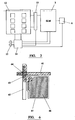
- Figure 1 shows in schematic cross-sectional view a liquid crystal cell 1 mounted on a thick film alumina hybrid substrate or chip carrier 2.
- the cell 1 is shown in exploded view in Figure 2.
- the use of a hybrid substrate for mounting electro-optic devices is discussed in more detail in our copending application PCT/GB99/04285, ref: P20957WO.
- Cell 1 comprises an active silicon backplane 3 in which a central region is formed to provide an array 4 of active mirror pixel elements arranged in 320 columns and 240 rows. Outside the array, but spaced from the edges of the backplane 3, is a peripheral glue seal 5, which seals the backplane 3 to the peripheral region of a front electrode 6.
- Figure 2 shows that the glue seal is broken to permit insertion of the liquid crystal material into the assembled cell, after which the seal is completed, either by more of the same glue, or by any other suitable material or means known per se.
- Front electrode 6 comprises a generally rectangular planar glass or silica substrate 7 coated on its underside, facing the backplane 3, with a continuous electrically conducting silk screened indium-tin oxide layer 8.
- a continuous electrically conducting silk screened indium-tin oxide layer 8 On one edge side of the substrate 7 is provided an evaporated aluminium edge contact 9, which extends round the edge of the substrate and over a portion of the layer 8, thereby providing an electrical connection to the layer 8 in the assembled cell 1.
- Insulating spacers 25 formed on the silicon substrate of the backplane 3 extend upwards to locate the front electrode 6 a predetermined, precise and stable distance from the silicon substrate, and liquid crystal material fills the space so defined. As described later, the spacers 25 and the backplane 3 are formed on the silicon substrate simultaneously with formation of the elements of the active backplane thereon, using all or at least some of the same steps.
- Figure 3 is a schematic outline of circuitry on the PCB 11 closely associated with operation of the cell 1, here shown schematically as backplane 3 and front electrode 6.
- Backplane 3 receives data from a memory 12 via an interface 13, and all of the backplane 3, front electrode 6, memory 12 and interface 13 are under the control of a programmable logic module 14 which is itself coupled to the parallel port of a PC via an interface 15.
- FIG 4 shows a general schematic view of the layout ("floorplan") of the active backplane 3.
- each one of the central array 4 of pixel active elements is composed essentially of an NMOS transistor having a gate connected to one of a set of a row conductors, a drain electrode connected to one of a set of column conductors and a source electrode or region which either is in the form of a mirror electrode or is connected to a mirror electrode.
- the rear located mirror electrode forms a liquid crystal pixel cell which has capacitive characteristics.
- Odd and even row conductors are connected to respective scanners 44, 45 spaced either side of the array.
- Each scanner comprises a level shifter 44b, 45b interposed between a shift register 44a, 45a and the array.
- a token signal is passed along the registers to enable (render the associated transistors conductive) individual rows in turn, and by suitable control of the registers different types of scan, e.g. interlaced or non-interlaced, can be performed as desired.
- Odd and even column conductors are connected to respective drivers 42, 43 spaced from the top and bottom of the array.
- Each driver comprises a 32 to 160 demultiplexer 42a, 43a feeding latches 42b, 43b, and a level shifter 42c, 43c between the latches and the column conductors.
- data from the memory 24 for successive sets of 32 odd or even column conductors is passed from sets of edge bonding pads 46, 47 to the demultiplexers 42a, 43a, and latched at 42b, 43b before being level shifted at 42c, 43c for supply as a driving voltage to the column conductors.
- Synchronisation between the row scanning and column driving ensures that the appropriate data driving voltage is applied via the enabled transistors of a row to the liquid crystal pixels, and for this purpose various control circuits 48 are provided.
- the active backplane is based on a p-type silicon substrate 51.
- the substrate 51 In the region of the array 4 it includes NMOS transistors 52, pixel mirrors 53 and the insulating spacer columns 25, and the substrate 51 is covered first by a lower substantially continuous silicon oxide layer 57 and then by an upper substantially continuous silicon oxide layer 58.
- Insulating ridges constructed similarly to the spacers and of similar height are formed outside the region of the array 41. The function of the insulating pillars and ridges is to ensure a constant and accurate spacing between the front electrode 22 and the silicon substrate 51, to prevent short circuits between the backplane and the front electrode and to provide electrical and optical uniformity and behaviour in the liquid crystal pixel array.
- Figure 5 is included merely to illustrate the different heights encountered in the backplane and that the other spatial arrangements of the elements do not necessarily correspond to what is found in practice.
- Figure 6 shows a plan view of an actual arrangement of transistor and mirror electrode, generally similar to that of Figure 5, but with the column 25 not shown. Transistors 52 are the highest part of the circuitry itself.
- the transistor 52 is further defined by a metallic gate electrode 59 on the layer 57 and a metallic drain electrode 60 on layer 58. Electrodes 59 and 60 are connected to a row conductor 61 and a column conductor 62 respectively.
- the layer 57 is modified to include a polysilicon region 56 spaced from the substrate 51 by a very thin gate oxide layer 55.
- the transistor source is in the form of a large diffusion region 63 within the layer 58 which is connected to electrode 65 of the pixel mirror 53, with the gate region 64 being located essentially under the crossover region of the column and row conductors 61, 62 to maximise the fill factor and to protect it from incident light.
- the pixel mirror is formed by the pixel electrode 65 on layer 58, which electrode is of the same metal as, and formed simultaneously with, the drain electrode 60. Beneath most of the mirror electrode 65 there is formed a depletion region 66 in the substrate 51. In the assembled device, the pixel electrodes are spaced from the opposed front electrode by somewhat less that 2 microns with smectic liquid crystal material 20 interposed.
- the pixel mirror is essentially flat, since there are no underlying discrete circuit elements, and occupies a proportion (fill factor) of around 65% of the pixel area.
- the need to maximise the fill factor is one consideration in the decision to employ a DRAM type backplane, rather than the SRAM type in which more space needs to be devoted to the two transistors and their associated elements.
- An insulating column or pillar 54 which is associated with each pixel extends above the topology of the rest of the backplane 21, but is also composed of the layers 57, 58 over the substrate 51, with a first metal film 67 between the layers 57, 58 and a second metal film 68 between layer 58 and (in use) the front electrode 22.
- First and second metal films 67, 68 are of the same metals, and deposited at the same time, as the electrodes 59, 60 of the transistor 52.
- the substrate is modified to provide a field oxide layer 69
- the bottom of layer 57 is modified to provide two polysilicon layers 70, 72 spaced by a thin oxide layer 71.
- the spacer provides good insulation between the front electrode and the active backplane.
- the spacer provides good insulation between the front electrode and the active backplane.
- a pixel cell thus formed has capacitance.
- Chiral smectic liquid crystal materials are ferroelectric, so that application of an electric field sufficient to cause realignment of the molecules is associated with an additional transfer of charge. This effect is associated with a time constant insofar as the liquid crystal material takes time to realign.
- the diffusion layer 66 forms in use a reverse biassed diode, the depletion region of which acts as the slug capacitance.
- the smectic liquid crystal used in the embodiment has a monostable alignment, so that for the DRAM type pixel element to remain in the switched state until it is next addressed, it is essential to limit charge leakage. In a sense, the fact that there is an additional charge displacement during realignment is helpful, in that the amount of charge leakage to permit relaxation to the original state is relatively large.
- illuminating light can penetrate to the backplane. If it reaches sensitive elements, photoconductivity can permit relaxation of the pixel in less time than the scanning period, and this should not be allowed to happen. Steps therefore need to be taken (a) to reduce light penetration to sensitive elements as far as possible; and (b) to alleviate the effects of any light which nevertheless still penetrates.
- step (a) is implemented insofar as the transistor 52, and particularly its gate region, is located substantially beneath metallic conductors 60, 61 and in that the diode provided by region 66, which is especially photosensitive, is largely hidden by the mirror layer 65. Further details regarding the slug capacitance and the avoidance of photoconductive effects will be found in our copending application PCT/GB99/04279, ref: P20960WO.
- the fill factor and reflectivity of the mirror electrode can be increased.
- top insulating layer is retained, but with vias extending to underlying electrode pads 65, which can be small as they no longer function as mirrors.
- a respective highly reflective mirror coating is deposited over the majority of the pixel area and is connected to its via.
- This construction has advantages, inter alia, of a high fill factor; a highly reflective mirror electrode; and reduced light penetration to the underlying semiconductor material. While it is preferred to retain the insulating columns and ridges to support and space the front electrode relative to the backplane, so reducing the fill factor slightly, these now include the additional top insulating layer.
- the only post-foundry step is the deposition of the reflective mirror material. It should be noted that the latter is not as flat as previously, owing to the underlying structure of the backplane.
- Full planarisation is a known process in which the topology of the backplane is effectively removed by filling with a insulating material, e.g. a polymer. Again, this may be implemented on the present backplane, with or without the top insulating layer introduced at the foundry, and with very flat highly reflective mirror electrodes deposited over each pixel with a high fill factor.
- a insulating material e.g. a polymer.
- the chiral smectic liquid crystal material is given a desired surface alignment at one or both substrates by means known per se.
- treatment will be of the partial or full planarisation layer if provided.
- Circuitry has a rectangular pixel array of 320 columns and 240 rows, the columns being supplied by parallel data lines and the rows being enabled to receive or act on the received data in turn in a desired sequence.
- the array is one half standard VGA resolution in each direction. It would be desirable to increase the resolution of the array to the VGA standard, and this is described later in respect to a modification
- the present embodiment of a smectic liquid crystal spatial light modulator may be driven at a line rate of at least 10MHz and a frame rate of up to 15 to 20kHz, requiring a data input of around 1 to 1.5 Gpixel per second.
- the pixel address time is around 100 nanoseconds
- the pixel will actually take around 1 to 5 microseconds to switch between optical states; and while overall frame writing time is of the order of 24 microseconds, the frame to frame writing period is around 80 microseconds.
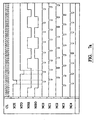
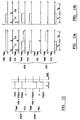
- a master clock operates at 50MHz. From the master clock pulses CL are derived in known manner the waveforms NTE, NTO, NISE, NISO, NC0 to NC4 shown in Figures 7 and 7a.
- the initial “N” indicates the use of negative logic in which signals are active in the low state. Where used, the inverse of these signals have the same terminology less the initial "N”.
- the final letters “E” and “O” refer to even and odd, as applied to rows or columns of the array.
- Figure 8 illustrates parts of the control circuits 48 of Figure 4.
- NSAR and NRAR for setting all rows (to blank the array) and resetting all rows (to permit rewriting of the array) respectively.
- Figure 8(a) indicates the derivation of 5 non-overlapping clocks (N)CC0 to (N)CC4 at the 10 MHz line frequency from the signals NC0 to NC4 when the signal NSAR is inactive, for use in controlling the column drivers 42, 43.
- a group of 32 incoming parallel data lines is 1:5 demultiplexed to the 160 even columns by driver 42 at the top of the array, and a complementary group of 32 incoming parallel data lines is 1:5 demultiplexed to the 160 odd columns by driver 43 at the foot of the array. Otherwise, drivers 42 and 43 are similarly arranged.
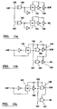
- Figure 9 shows one of 32 similar circuits of the driver 42, each for a respective single column in the first set of 32 even columns.
- a data signal DD from an input 131 coupled to a respective one of the 32 input data lines is transmitted by a gate 132 during the active period of clock NCC0 and held on the gate capacitor of an inverter 133 until a gate 134 controlled by clock pulse NCC4 permits transmission of the signal to a latch 135.
- Latch 135 is bistable and consists essentially of two inverters coupled in a ring via a further gate 136 also controlled by the gate pulse CC4, so that the ring is opened when the signal is being transmitted to the latch via the gate 134, and thereafter closed to hold the signal at the latch output.
- the output of the latch is connected to the column conductor via a level shifter 137 and two series coupled buffers 138.
- This overall arrangement for the first set of column conductors is replicated for the remaining four sets, with the same 32 input data lines but with respective different clock signals NCC1 to NCC4 on the first gate 132 as appropriate.
- the signals applied to the gates 134 and 136 remain as NCC4 and CC4, so that data signals for a whole line are applied simultaneously to all 320 columns in response to the signal NCC4, and are maintained thereat until the next pulse NCC4.
- NSAR When NSAR is active, it over-rides the clock pulses NCC0 to NCC4, making all 320 columns available to the 64 data input lines simultaneously.
- Figure 8(b) shows the derivation of 5 non-overlapping clocks (N)CR0 to (N)CR4 at the 10 MHz line frequency from the signals NC0 to NC4 when the signal NISE or NISO is inactive, for use in controlling the row drivers 44, 45.
- Figure 10 shows a single stage of the odd row scanner 44 of the preferred embodiment, including an associated level shifter unit 141 of the level shifter 44b coupled between a single stage 140 of the shift register 44a and two buffers 149.
- the even row scanner 45 is arranged in a similar manner.
- the stage 140 comprises a pair of inverting logic gates 143, 144 coupled in a ring via a transmission gate 145.
- the input 142 of logic gate 143 is commonly coupled to the output of the gate 145 and to the output of a transmission gate 146 which acts to receive the output 147 (token NTE) from a preceding stage in the register.
- Gates 145 and 146 are respectively enabled by inverse clock signals NCR0 and CRO, whereby the ring is broken as the signal from transmission gate 146 is passed to the input of gate 143, and subsequently reformed to maintain the inverse of the received signal at an output point 148.
- Gates 143', 144', 145' and 146' are arranged in similar manner to the gates 143 to 146, and act similarly but in response to clock pulses NCR4, CR4, whereby the inverse of the signal at point 148 is held at output point 148', where it is level shifted by circuit 121 and transmitted to the respective row. Thus each row is enabled in turn in response to the signal NCR4.
- Each of gates 143, 144 and 144' is a NAND gate with two inputs, and the gate 143' is a NAND gate with 3 inputs.
- the second input to gates 143 and 144' is the signal NSAR
- the second input to gates 143' and 144 is the signal NRAR
- the third input to gate 143' is a signal NCR2'.
- the signal NCR2' is derived as shown in Figure 8(c). It is similar to signal NCR2 but is over-ridden when signal NSAR is active. When NSAR is inactive, the effect of the clock signal NCR2 is to ensure that the second ring is reset and the row disabled before the following row is enabled, thus ensuring that data supply is to a single row, and that there can be no overlap of the same data between rows.
- the control signal NSAR acts to disable the signal NCR2' and to set (latch) all outputs of the register, thereby enabling all rows for blanking in the manner described at the commencement of this section.
- the control signal NRAR subsequently acts to turn all the rows off again.
- the signal NSAR over-rides the normal operation of the shift registers.
- the action of the signal NSAR is thus (a) to over-ride the column clocks NCC0 to NCC5 so that all five sets of columns are simultaneously provided with data from the 64 data inputs, and (b) to disable the clock pulse NCR2' and the normal action of the register, and to latch all rows. This permits the entire array of pixels to be blanked simultaneously.
- the signals NISE and NISO are complementary. When active, their action is to inhibit the production of the row clock pulses (N)CR0 to (N)CR4, Figure 8(b). In this manner only one of the shift registers 44a, 44b is active at any one time, making it possible to control the manner in which the tokens are passed down the rows. For example, if, as shown, NISE and NISO are derived so as to have one half line frequency, the registers are enabled alternately to provided a progressive or non-interlaced line scan down the array. An alternative would be to provide signals NISE and NISO in the form of pulses of one half the frame address period, so that the one register is completely scanned and then the other register is completely scanned, thus providing an interlaced scan.
- shift register stages are adapted to provide directly for a response to the signals NSAR and NRAR
- alternative means could be provided as a separate entity between the registers and the rows, for example an OR gate for NSAR and an AND gate for NRAR coupled in series between a register output and the associated row.
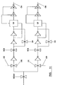
- the single pixel mirror and active element is replaced by a group of four (two by two), with a corresponding doubling of the row and column address lines.
- the column drivers and row scanners are provided with 1:2 demultiplexers.
- the column circuits are merely doubled in number, each pair CA and CB being enabled in alternation by transmission gates 150, 151, with complementarily driven control inputs 152, 153 as illustrated schematically in Figure 11.
- Figure 12a to 12c illustrate three possible schemes for the row scanners.
- logic gates 160, 161 are disposed between the output point 148' and respective level shifters 141 and buffers 149. Second inputs 162, 163 of the gates are driven in complementary fashion to enable either the upper or lower pair of pixels RU and RL.
- the demultiplexing may be performed after the level shifter 141, respectively at gates 164, 165 between the level shifters 141 and final output stages 149', or at gates 166, 167 which also constitute the final output stage.
- the ratio of mirror area to pixel area is reduced, and care needs to be taken to shield the underlying active elements from incident light.
- the ratio of total pixel capacitance to liquid crystal cell capacitance is also somewhat reduced, from 10:1 to 8.4:1. Nevertheless, the trade-off with increased resolution is considered overall not to be disadvantageous.
- Spatial light modulation provides opportunities both in optical processing, for example in holographic and switching applications, where requirements are commonly very stringent in terms of factors such as timings, continuity of illumination, length of viewing, etc. Set against this, most optical processing requires only binary modulation across the image plane.
- the spatial light modulator of the preferred embodiment may be driven, due in part to the versatility afforded by the active backplane design.
- the front electrode can be driven alternately to V and zero, with the backplane being synchronously controlled so as to turn selected pixels optically on during one frame scan and to turn other selected pixels optically off during the other frame scan.
- the voltage applied to each pixel is higher, at V, thus increasing switching speed, but with the need to perform two frame scans to complete data entry.
- one-pass and two-pass respectively.
- the one-pass scheme permits a somewhat higher frame rate at the greatest usable voltages.
- One Pass Scheme Figure 13 illustrates voltage waveforms which can be used in a one pass scheme when the front electrode voltage VFE is at V/2.
- the voltage Vpad at mirror electrodes of pixels DUP in an addressed line which are to be turned from off to on are driven to a value V from the column electrodes, and for pixels UDP which are to be turned from on to off the mirror electrodes are driven to zero voltage.
- the resulting voltage across the liquid crystal cell is VLC.
- Energisation typically takes around 10ns, although 100ns is actually allowed in the embodiment.
- a significantly longer period T is allowed for the pixels actually to switch, following which all pixel electrode voltages (Vpad) are returned to voltage V/2 by altering the voltage to the level shifters and either performing a second scan or a set/reset operation using the signals NSAR and NRAR to gate all pixel transistors on and off, as shown in Figure 13a. Returning the pixels to V/2 ensures that the length of application of dc is well defined and repeatable.
- pulse 131 denotes selection of an individual row
- T L denotes the time to load the array (including a period for the liquid crystal to settle)
- T R is the time over which the image is read, the start only of this period being shown.
- Pulse 132 denotes either selection of an individual row during a second scan, or a global row select for the set/reset option.
- the set/reset option is faster, and is preferred. While the length of application of dc to all pixels differs from row to row when using the set/reset option, due to the finite time taken to write the array, this is immaterial since the length of application of dc pulses to the same pixel is equal from frame to frame, and this is the important factor when contemplating dc balance. In either case, the transistor is subsequently turned off, permitting electrostatic stabilisation (see later).
- Two-Pass Scheme Figure 14 shows voltage waveforms which could be used in a two-pass scheme, over the two frame scan periods or passes P1 and P2 necessary to write the whole array.
- first pass P1 selected pixels are addressed to turn them optically on
- second pass P2 selected pixels are addressed to turned them optically off.
- all voltages are zero dc, optionally with a low level ac voltage for ac stabilisation of the switched states.
- Plot (i) shows the voltage VFE at the front electrode, which is raised to V volts only for the duration of the second pass P2.
- Plots (ii) and (iii) are plots of the voltage Vpad at pixel mirror pads which are respectively being turned ON or OFF.
- any pad may be switched from zero volts to V volts.
- a first global blank BV is applied to drive all mirror pads to V volts between the two passes.
- any pad may be switched from V volts to zero volts.
- a second global blank B0 is applied to drive all pads to zero volts at the end of the second pass. Blanks BV and B0 are applied in substantial synchronism with the switching of the second (front) electrode.
- Plot (ii) shows the voltage at a pad for a selected pixel which is to be turned on during the row scanning of the first pass, so providing a positive potential difference pulse across the associated liquid crystal element as shown in plot (iv).
- the first global blank BV in association with the switching of VFE acts to reduce the potential difference across all liquid crystal elements to zero regardless of whether they have been switched or not, with both sides of the liquid crystal cells now at V volts.
- Plot (iii) shows the voltage at a pad for a selected pixel which is to be turned off during the row scanning of the second pass, so providing a negative potential difference across the associated liquid crystal element as shown in plot (v).
- the second global blank B0 in association with the switching of VFE acts to reduce the potential difference across all liquid crystal elements to zero regardless of whether they have been switched or not, with both sides of the liquid crystal cells now at zero volts.
- BV and B0 are substantially synchronous with the switching of VFE, so that these pixels experience zero potential difference throughout the two passes. In all cases the timing of BV and B0 relative to VFE must be such that no unwanted switching of pixels occurs.
- Figure 15 shows simplified voltage waveforms which could be used in a similar two-pass scheme, over first and second frame scan periods or passes P1 and P2 necessary to write the whole array.
- P1 selected pixels are addressed to turn them optically on
- P2 pixels are addressed to turned them optically off.
- all voltages are zero dc, optionally with a low level ac voltage for ac stabilisation of the switched states.
- Plot (i) shows the voltage VFE at the front electrode, which is raised to V volts only for the duration of P1.
- Plot (ii) is a general plot of the voltage Vpad obtainable at any pixel mirror pad.
- any pad may be switched from zero volts to V volts.
- a first global blank BV is applied to drive all mirror pads to V volts between P1 and P2.
- a second global blank B0 is applied to drive all pads to zero volts at the end of the second pass. Blanks BV and B0 are applied in synchronism with the switching of the second electrode.
- Plot (iii) shows the voltage at a pad for a selected pixel which is to be turned on during the row scanning of P1, so providing a positive potential difference pulse across the associated liquid crystal element as shown in plot (iv).
- the first global blank BV in association with the switching of VFE acts to reduce the potential difference across all liquid crystal elements to zero regardless of whether they have been switched or not, with both sides of the liquid crystal cells now at V volts.
- Plot (v) shows the voltage at a pad for a selected pixel which is to be turned off during the row scanning of P2, so providing a negative potential difference across the associated liquid crystal element as shown in plot (vi).
- the second global blank B0 in association with the switching of VFE acts to reduce the potential difference across all liquid crystal elements to zero regardless of whether they have been switched or not, with both sides of the liquid crystal cells now at zero volts.
- Plot (vii) shows the voltage pulse at a pad for any pixel which (as an option) is not addressed during either P1 or P2, and which is due solely to the effect of the blanks BV and B0.
- BV and B0 are substantially synchronous with the switching of VFE, so that these pixels experience zero potential difference throughout the two passes. In all cases the timing of BV and B0 relative to VFE must be such that no unwanted switching of pixels occurs.
- P1 and P2 have been shown as immediately succeeding one another, as is preferred, this is not entirely necessary so long as the scheme is consistent with the required pixel switchings. For example, there could be a small delay between P1 and P2 to enable the last addressed pixels to switch completely. In such a case it would be desirable to apply BV and the switching of VFE synchronously with the commencement of P2.
- a binary image may be written from a blank image or an existing image, by a 1-pass method as has been described above
- the time averaged optical image is zero if the positive and reverse images are held for equal times, so it may well be necessary to interrupt the illumination (or the viewing step) in order to see a positive image.
- a two-pass scheme for example of the type illustrated in Figure 14, can be operated in a number of ways.
- an existing image may be replaced by a new image simply by turning all appropriate pixels on during the first pass, and by turning the complementary set of pixels off during the second pass (as in Figure 14), i.e. all "1"s in the new image are first addressed, regardless of whether the pixel is already “1”, and subsequently all "0"s in the new image are addressed regardless of whether the pixel is already "0". No pixel is unaddressed.
- any liquid crystal element is only driven on or off when a change of state therein is required, otherwise it remains unaddressed and follows plot (vii).
- Each pixel is therefore subjected only to alternate turn-on and turn-off pulses of well-defined and equal lengths, thus automatically affording de balance in the long term.
- This type of scheme is disclosed International Patent Application No. WO 92/04710 mentioned previously.
- This scheme also requires a determination of the differences between the existing image and the required image in order that the pixels to be driven in each of the two passes may be determined.
- the advantage of automatic long term dc balance is partially offset by increased computational difficulty relative to the first two-pass scheme.
- a third and preferred scheme which is a modification of the two-pass scheme of Figure 14, and which is illustrated in Figure 17, enables a series of binary images to be written in succession, with de balance, and with fast or driven erasure.
- Plots (iii) and (iv) of Figure 17 illustrate mirror pad voltages and pixels potential differences for a pixel which is selected. This scheme is in accordance with the invention, with alternate blank images.
- a first image is written from a blank array of elements, by controlling the writing process so that only those elements which need to be turned on are driven (during the period A of plot (ii)), all other elements receiving zero volts.
- the WRITE step is followed, preferably immediately at time t1, by a first global blank B0 to zero volts, and VFE remains at zero volts, as a shown in plot (i) of Figure 16.
- the required binary image remains unaltered.
- Subsequent erasure to a blank array is then effected during an ERASE period t2 to t3 by writing the negative image to the written pixels only. This is effected by applying a second global blank BV to V volts at time t2, synchronously with switching of VFE, and then during a period B addressing only those elements which were previously turned on, the other elements again receiving zero volts. At t3, a third global blank B0 to zero volts is applied synchronously with switching to zero volts of VFE.
- the erasure step is therefore generally similar to the second pass of Figure 14.
- the driven elements alternately receive opposed voltages to provide dc balance, and the other unselected elements receive no voltage and so remain balanced.
- time t3 it is possible to commence the writing of another binary image, and, as illustrated, this may commence substantially at time t3.
- this third two-pass scheme resembles the second two-pass scheme above in that the full voltage V can be applied in different directions during the two passes of writing and erasure, but differs therefrom in that it is the same group of selected pixels which are addressed each time rather than different non-complementary groups, so reducing computational requirements. It differs from the one-pass method in which all elements are necessarily driven one way or the other during the frame scan.
- a further consideration is that while the writing stage may be followed by a period of time during which the image is "viewed" or utilised, there is no need to hold the blank image obtained after erasure for any length of time. As particularly illustrated in Figure 17, once all the pixels have switched back to their initial state, a further writing stage may commence immediately. Since the ratio of the IMAGE period to the WRITE and ERASE periods times may be large, the image is available for a large fraction of the total time, and its contrast ratio is correspondingly improved.
- Grey Scales Temporal digital modulation to achieve a grey scale effect is known, using multiple bit planes representative of a sequence of binary images.
- the effective duration of the binary images is such that temporal integration thereof, for example by a viewer, gives the grey scale image.
- the production of effective grey scales is best effected by the use of weighted bit planes where possible.
- the grey scale image is decomposed into multiple binary images (bit planes) of differing duration such that temporal integration thereof, for example by a viewer, gives the grey scale image.
- the decomposition of the grey scale image and the corresponding durations of the bit planes are typically on a binary basis, although other weightings could be used.
- the different bit planes for a grey scale image can be stored as sequential binary strings in a computer, and will be read out one at a time in any desired order after which they can be discarded unless the image needs to be repeated. It is computationally easiest to read out the bit planes in the order in which they have been stored, since then the only address which needs to be stored is the starting address of the first stored bit planes, all bit planes then being read out one at a time simply by clocking out a predetermined number of data bits in sequence for each bit planes.
- bit planes that have been read by the bit planes for a succeeding image it might be possible immediately to replace bit planes that have been read by the bit planes for a succeeding image, particularly where the bit planes are being produced in real time. However, under other circumstances this could be difficult, and the set of bit planes for a successive image will then normally be stored elsewhere. In certain cases it would be possible to provide storage for just two bit planes one of which is written while the other is being read, and vice versa.
- each bit plane is read from memory, it is then written, e.g. using the single pass scheme described above, and viewed over a period corresponding to its weighting so that the eye synthesises the intended grey scale image.
- the single pass scheme is preferred insofar as it merely over-writes the preceding bit frame without the need for a second pass, the associated front electrode switching and blanking pulses. The avoidance of lost time between successive valid images enables continuous illumination and the easier provision of bit frames of an accurately weighted duration.
- each pixel is subjected to a series of voltage pulses according to the point in the grey scale it represents (as in the number representing the grey scale level, and usually but not necessarily in that order).
- Each applied voltage may be of the same or opposed polarity compared to the preceding voltage, and the same number of voltage pulses, equal to the number of bit planes (ignoring polarity), is applied to each pixel to synthesise the image.
- each pixel can be represented by a corresponding 6 digit binary number.
- double pass schemes could alternatively be adapted for use in multiple or weighted bit plane schemes.
- each binary bit plane by any of the binary imaging methods described in the preceding section which itself produces dc balance - for example by starting from a blank image, writing, viewing and erasing the binary image by selective energisation (+V) and driven blanking (-V) of selected pixels only.
- the actual duration of the binary image is not directly proportional to the time allocated thereto, for example because of intervening blanking steps, etc., leading to a degree of distortion in the binary nature of the bitplane periods, and hence the perceived grey scale values. While this could be compensated for if desired, it represents an additional complication.
- the array of the invention may be used in any cell construction irrespective of whether or not the cell is intended to function as a light modulator or display, and irrespective of whether or not the contents of the cell are intended to have a liquid crystal phase.
- grey scale is used herein, it should be made clear that the term is used in relation to any colour, including white.
- methods, arrays, backplanes, circuitry etc. of the invention are described in relation to a single colour (monochrome images), including white, it is envisaged that variable colour images or displays etc. will be produced in manners known per se, such as by spatially subdividing a single array into different colour pixels, superimposing displays from differently coloured monochrome arrays for example by projection, or temporal multiplexing, for example sequential projection of red green and blue images.
Landscapes
- Engineering & Computer Science (AREA)
- Chemical & Material Sciences (AREA)
- Crystallography & Structural Chemistry (AREA)
- Physics & Mathematics (AREA)
- Computer Hardware Design (AREA)
- General Physics & Mathematics (AREA)
- Theoretical Computer Science (AREA)
- Liquid Crystal (AREA)
- Liquid Crystal Display Device Control (AREA)
- Control Of Indicators Other Than Cathode Ray Tubes (AREA)
Applications Claiming Priority (3)
| Application Number | Priority Date | Filing Date | Title |
|---|---|---|---|
| GBGB9827945.8A GB9827945D0 (en) | 1998-12-19 | 1998-12-19 | Method of driving a spatial light modulator |
| GB9827945 | 1998-12-19 | ||
| PCT/GB1999/004275 WO2000038167A1 (en) | 1998-12-19 | 1999-12-16 | Methods of driving an array of optical elements |
Publications (2)
| Publication Number | Publication Date |
|---|---|
| EP1141934A1 EP1141934A1 (en) | 2001-10-10 |
| EP1141934B1 true EP1141934B1 (en) | 2006-10-25 |
Family
ID=10844518
Family Applications (1)
| Application Number | Title | Priority Date | Filing Date |
|---|---|---|---|
| EP99962327A Expired - Lifetime EP1141934B1 (en) | 1998-12-19 | 1999-12-16 | Methods of driving an array of optical elements |
Country Status (8)
| Country | Link |
|---|---|
| US (1) | US6762873B1 (https=) |
| EP (1) | EP1141934B1 (https=) |
| JP (1) | JP2002533768A (https=) |
| AU (1) | AU1870500A (https=) |
| CA (1) | CA2353819A1 (https=) |
| DE (1) | DE69933790T2 (https=) |
| GB (1) | GB9827945D0 (https=) |
| WO (1) | WO2000038167A1 (https=) |
Families Citing this family (64)
| Publication number | Priority date | Publication date | Assignee | Title |
|---|---|---|---|---|
| US6674562B1 (en) | 1994-05-05 | 2004-01-06 | Iridigm Display Corporation | Interferometric modulation of radiation |
| US7138984B1 (en) | 2001-06-05 | 2006-11-21 | Idc, Llc | Directly laminated touch sensitive screen |
| US7471444B2 (en) | 1996-12-19 | 2008-12-30 | Idc, Llc | Interferometric modulation of radiation |
| WO1999052006A2 (en) | 1998-04-08 | 1999-10-14 | Etalon, Inc. | Interferometric modulation of radiation |
| US8928967B2 (en) | 1998-04-08 | 2015-01-06 | Qualcomm Mems Technologies, Inc. | Method and device for modulating light |
| WO2003007049A1 (en) | 1999-10-05 | 2003-01-23 | Iridigm Display Corporation | Photonic mems and structures |
| US6781742B2 (en) * | 2000-07-11 | 2004-08-24 | Semiconductor Energy Laboratory Co., Ltd. | Digital micromirror device and method of driving digital micromirror device |
| TW535966U (en) * | 2001-02-02 | 2003-06-01 | Koninkl Philips Electronics Nv | Display device |
| GB0121308D0 (en) | 2001-09-03 | 2001-10-24 | Thomas Swan & Company Ltd | Optical processing |
| US7071908B2 (en) | 2003-05-20 | 2006-07-04 | Kagutech, Ltd. | Digital backplane |
| JP3974093B2 (ja) * | 2003-08-21 | 2007-09-12 | シャープ株式会社 | 表示装置 |
| US7142346B2 (en) | 2003-12-09 | 2006-11-28 | Idc, Llc | System and method for addressing a MEMS display |
| US7161728B2 (en) | 2003-12-09 | 2007-01-09 | Idc, Llc | Area array modulation and lead reduction in interferometric modulators |
| JP2006065272A (ja) * | 2004-07-28 | 2006-03-09 | Sony Corp | ホログラム装置、空間光変調器と撮像素子の位置決め方法及びホログラム記録材料 |
| US7560299B2 (en) * | 2004-08-27 | 2009-07-14 | Idc, Llc | Systems and methods of actuating MEMS display elements |
| US7551159B2 (en) * | 2004-08-27 | 2009-06-23 | Idc, Llc | System and method of sensing actuation and release voltages of an interferometric modulator |
| US7515147B2 (en) | 2004-08-27 | 2009-04-07 | Idc, Llc | Staggered column drive circuit systems and methods |
| US7889163B2 (en) | 2004-08-27 | 2011-02-15 | Qualcomm Mems Technologies, Inc. | Drive method for MEMS devices |
| US7499208B2 (en) | 2004-08-27 | 2009-03-03 | Udc, Llc | Current mode display driver circuit realization feature |
| US7602375B2 (en) | 2004-09-27 | 2009-10-13 | Idc, Llc | Method and system for writing data to MEMS display elements |
| US7920135B2 (en) | 2004-09-27 | 2011-04-05 | Qualcomm Mems Technologies, Inc. | Method and system for driving a bi-stable display |
| US7317568B2 (en) | 2004-09-27 | 2008-01-08 | Idc, Llc | System and method of implementation of interferometric modulators for display mirrors |
| US7679627B2 (en) * | 2004-09-27 | 2010-03-16 | Qualcomm Mems Technologies, Inc. | Controller and driver features for bi-stable display |
| US7545550B2 (en) | 2004-09-27 | 2009-06-09 | Idc, Llc | Systems and methods of actuating MEMS display elements |
| US7532195B2 (en) * | 2004-09-27 | 2009-05-12 | Idc, Llc | Method and system for reducing power consumption in a display |
| US7583429B2 (en) | 2004-09-27 | 2009-09-01 | Idc, Llc | Ornamental display device |
| US7369294B2 (en) | 2004-09-27 | 2008-05-06 | Idc, Llc | Ornamental display device |
| US7345805B2 (en) | 2004-09-27 | 2008-03-18 | Idc, Llc | Interferometric modulator array with integrated MEMS electrical switches |
| US8878825B2 (en) | 2004-09-27 | 2014-11-04 | Qualcomm Mems Technologies, Inc. | System and method for providing a variable refresh rate of an interferometric modulator display |
| US7136213B2 (en) | 2004-09-27 | 2006-11-14 | Idc, Llc | Interferometric modulators having charge persistence |
| US7653371B2 (en) | 2004-09-27 | 2010-01-26 | Qualcomm Mems Technologies, Inc. | Selectable capacitance circuit |
| US8310441B2 (en) | 2004-09-27 | 2012-11-13 | Qualcomm Mems Technologies, Inc. | Method and system for writing data to MEMS display elements |
| US7535466B2 (en) | 2004-09-27 | 2009-05-19 | Idc, Llc | System with server based control of client device display features |
| CN100439967C (zh) | 2004-09-27 | 2008-12-03 | Idc公司 | 用于多状态干涉光调制的方法和设备 |
| US7586484B2 (en) | 2004-09-27 | 2009-09-08 | Idc, Llc | Controller and driver features for bi-stable display |
| US7626581B2 (en) | 2004-09-27 | 2009-12-01 | Idc, Llc | Device and method for display memory using manipulation of mechanical response |
| US8514169B2 (en) | 2004-09-27 | 2013-08-20 | Qualcomm Mems Technologies, Inc. | Apparatus and system for writing data to electromechanical display elements |
| US7446927B2 (en) | 2004-09-27 | 2008-11-04 | Idc, Llc | MEMS switch with set and latch electrodes |
| US7675669B2 (en) * | 2004-09-27 | 2010-03-09 | Qualcomm Mems Technologies, Inc. | Method and system for driving interferometric modulators |
| US7843410B2 (en) | 2004-09-27 | 2010-11-30 | Qualcomm Mems Technologies, Inc. | Method and device for electrically programmable display |
| US7460246B2 (en) | 2004-09-27 | 2008-12-02 | Idc, Llc | Method and system for sensing light using interferometric elements |
| US7808703B2 (en) | 2004-09-27 | 2010-10-05 | Qualcomm Mems Technologies, Inc. | System and method for implementation of interferometric modulator displays |
| US7724993B2 (en) | 2004-09-27 | 2010-05-25 | Qualcomm Mems Technologies, Inc. | MEMS switches with deforming membranes |
| US7310179B2 (en) | 2004-09-27 | 2007-12-18 | Idc, Llc | Method and device for selective adjustment of hysteresis window |
| US7948457B2 (en) | 2005-05-05 | 2011-05-24 | Qualcomm Mems Technologies, Inc. | Systems and methods of actuating MEMS display elements |
| CA2607807A1 (en) | 2005-05-05 | 2006-11-16 | Qualcomm Incorporated | Dynamic driver ic and display panel configuration |
| US7920136B2 (en) | 2005-05-05 | 2011-04-05 | Qualcomm Mems Technologies, Inc. | System and method of driving a MEMS display device |
| US7355779B2 (en) | 2005-09-02 | 2008-04-08 | Idc, Llc | Method and system for driving MEMS display elements |
| US8391630B2 (en) | 2005-12-22 | 2013-03-05 | Qualcomm Mems Technologies, Inc. | System and method for power reduction when decompressing video streams for interferometric modulator displays |
| US7916980B2 (en) | 2006-01-13 | 2011-03-29 | Qualcomm Mems Technologies, Inc. | Interconnect structure for MEMS device |
| US8194056B2 (en) | 2006-02-09 | 2012-06-05 | Qualcomm Mems Technologies Inc. | Method and system for writing data to MEMS display elements |
| US7582952B2 (en) | 2006-02-21 | 2009-09-01 | Qualcomm Mems Technologies, Inc. | Method for providing and removing discharging interconnect for chip-on-glass output leads and structures thereof |
| US7903047B2 (en) | 2006-04-17 | 2011-03-08 | Qualcomm Mems Technologies, Inc. | Mode indicator for interferometric modulator displays |
| US8049713B2 (en) | 2006-04-24 | 2011-11-01 | Qualcomm Mems Technologies, Inc. | Power consumption optimized display update |
| US7702192B2 (en) | 2006-06-21 | 2010-04-20 | Qualcomm Mems Technologies, Inc. | Systems and methods for driving MEMS display |
| US7777715B2 (en) | 2006-06-29 | 2010-08-17 | Qualcomm Mems Technologies, Inc. | Passive circuits for de-multiplexing display inputs |
| US7576815B2 (en) * | 2006-07-10 | 2009-08-18 | Intel Corporation | Method and apparatus of liquid-crystal-on-silicon assembly |
| US7957589B2 (en) * | 2007-01-25 | 2011-06-07 | Qualcomm Mems Technologies, Inc. | Arbitrary power function using logarithm lookup table |
| US8405649B2 (en) * | 2009-03-27 | 2013-03-26 | Qualcomm Mems Technologies, Inc. | Low voltage driver scheme for interferometric modulators |
| US8736590B2 (en) | 2009-03-27 | 2014-05-27 | Qualcomm Mems Technologies, Inc. | Low voltage driver scheme for interferometric modulators |
| US20110109615A1 (en) * | 2009-11-12 | 2011-05-12 | Qualcomm Mems Technologies, Inc. | Energy saving driving sequence for a display |
| US8547623B2 (en) * | 2011-11-22 | 2013-10-01 | Sharp Kabushiki Kaisha | Dual-mode electrowetting display device |
| GB2504970A (en) | 2012-08-15 | 2014-02-19 | Swan Thomas & Co Ltd | Optical device and methods to reduce cross-talk |
| WO2016067154A1 (ja) | 2014-10-29 | 2016-05-06 | 株式会社半導体エネルギー研究所 | 表示素子、表示装置、または電子機器 |
Family Cites Families (8)
| Publication number | Priority date | Publication date | Assignee | Title |
|---|---|---|---|---|
| US4859035A (en) * | 1986-05-26 | 1989-08-22 | Nec Corporation | Ferroelectric liquid crystal light shutter device and method of controlling the driving of the same |
| GB2247973B (en) * | 1990-09-11 | 1994-07-27 | Stc Plc | Co-ordinate addressing of liquid crystal cells |
| GB2247974B (en) * | 1990-09-11 | 1994-07-27 | Stc Plc | Co-ordinate addressing of liquid crystal cells |
| US5774104A (en) * | 1990-09-11 | 1998-06-30 | Northern Telecom Limited | Co-ordinate addressing of liquid crystal cells |
| JPH07191304A (ja) | 1993-12-25 | 1995-07-28 | Semiconductor Energy Lab Co Ltd | 液晶電気光学装置 |
| JPH08221039A (ja) * | 1995-02-17 | 1996-08-30 | Sony Corp | 液晶表示装置及びその駆動方法 |
| US5959598A (en) * | 1995-07-20 | 1999-09-28 | The Regents Of The University Of Colorado | Pixel buffer circuits for implementing improved methods of displaying grey-scale or color images |
| GB2321754A (en) * | 1997-01-31 | 1998-08-05 | Sharp Kk | Diffractive spatial light modulator |
-
1998
- 1998-12-19 GB GBGB9827945.8A patent/GB9827945D0/en not_active Ceased
-
1999
- 1999-12-16 EP EP99962327A patent/EP1141934B1/en not_active Expired - Lifetime
- 1999-12-16 WO PCT/GB1999/004275 patent/WO2000038167A1/en not_active Ceased
- 1999-12-16 CA CA002353819A patent/CA2353819A1/en not_active Abandoned
- 1999-12-16 DE DE69933790T patent/DE69933790T2/de not_active Expired - Lifetime
- 1999-12-16 JP JP2000590154A patent/JP2002533768A/ja active Pending
- 1999-12-16 US US09/868,217 patent/US6762873B1/en not_active Expired - Lifetime
- 1999-12-16 AU AU18705/00A patent/AU1870500A/en not_active Abandoned
Also Published As
| Publication number | Publication date |
|---|---|
| DE69933790D1 (de) | 2006-12-07 |
| EP1141934A1 (en) | 2001-10-10 |
| DE69933790T2 (de) | 2007-10-04 |
| WO2000038167A1 (en) | 2000-06-29 |
| GB9827945D0 (en) | 1999-02-10 |
| AU1870500A (en) | 2000-07-12 |
| US6762873B1 (en) | 2004-07-13 |
| CA2353819A1 (en) | 2000-06-29 |
| JP2002533768A (ja) | 2002-10-08 |
Similar Documents
| Publication | Publication Date | Title |
|---|---|---|
| EP1141934B1 (en) | Methods of driving an array of optical elements | |
| EP1145217B1 (en) | Active backplane circuitry, spatial light modulator comprising such a circuitry, and method of operating such a spatial light modulator | |
| JP2002533767A5 (https=) | ||
| JP2002533768A5 (https=) | ||
| TW559752B (en) | Liquid crystal display device, drive circuit, drive method and electronic equipment | |
| TW550413B (en) | Method for driving display apparatus, driving circuit, display apparatus and electronic machine | |
| WO2004095404A2 (en) | Display system with frame buffer and power saving sequence | |
| JPH06313876A (ja) | 液晶表示装置の駆動方法 | |
| TW583616B (en) | Liquid crystal driving devices | |
| US10553167B2 (en) | Display device | |
| JPH10197894A (ja) | 液晶表示装置及び液晶表示装置の駆動方法 | |
| JP2004029477A (ja) | 液晶表示装置の駆動方法及び液晶表示装置 | |
| TWI248055B (en) | LCD device and display method thereof | |
| EP1147453B1 (en) | Spacers for cells having spaced opposed substrates | |
| US9250460B2 (en) | Liquid crystal display comprising erase electrodes | |
| KR100631228B1 (ko) | 전기 광학 장치, 그 구동 회로 및 구동 방법, 및 전자기기 | |
| US6812909B1 (en) | Active semiconductor backplanes | |
| JPH08241060A (ja) | 液晶表示装置及びその駆動方法 | |
| TW563082B (en) | Antiferroelectric liquid crystal devices, method and system for driving an antiferroelectric liquid crystal display device | |
| US20190311684A1 (en) | Display device | |
| US11978506B2 (en) | Spatial light modulator | |
| US6630919B1 (en) | Optical modulator and integrated circuit therefor | |
| JPS629320A (ja) | 表示装置 | |
| JPS617828A (ja) | 液晶素子の駆動法 |
Legal Events
| Date | Code | Title | Description |
|---|---|---|---|
| PUAI | Public reference made under article 153(3) epc to a published international application that has entered the european phase |
Free format text: ORIGINAL CODE: 0009012 |
|
| 17P | Request for examination filed |
Effective date: 20010609 |
|
| AK | Designated contracting states |
Kind code of ref document: A1 Designated state(s): AT BE CH CY DE DK ES FI FR GB GR IE IT LI LU MC NL PT SE |
|
| RBV | Designated contracting states (corrected) |
Designated state(s): DE FR GB NL |
|
| 17Q | First examination report despatched |
Effective date: 20040812 |
|
| GRAP | Despatch of communication of intention to grant a patent |
Free format text: ORIGINAL CODE: EPIDOSNIGR1 |
|
| GRAS | Grant fee paid |
Free format text: ORIGINAL CODE: EPIDOSNIGR3 |
|
| RAP1 | Party data changed (applicant data changed or rights of an application transferred) |
Owner name: QINETIQ LIMITED |
|
| GRAA | (expected) grant |
Free format text: ORIGINAL CODE: 0009210 |
|
| AK | Designated contracting states |
Kind code of ref document: B1 Designated state(s): DE FR GB NL |
|
| REG | Reference to a national code |
Ref country code: GB Ref legal event code: FG4D |
|
| REF | Corresponds to: |
Ref document number: 69933790 Country of ref document: DE Date of ref document: 20061207 Kind code of ref document: P |
|
| ET | Fr: translation filed | ||
| PLBE | No opposition filed within time limit |
Free format text: ORIGINAL CODE: 0009261 |
|
| STAA | Information on the status of an ep patent application or granted ep patent |
Free format text: STATUS: NO OPPOSITION FILED WITHIN TIME LIMIT |
|
| 26N | No opposition filed |
Effective date: 20070726 |
|
| PGFP | Annual fee paid to national office [announced via postgrant information from national office to epo] |
Ref country code: NL Payment date: 20081118 Year of fee payment: 10 |
|
| REG | Reference to a national code |
Ref country code: NL Ref legal event code: V1 Effective date: 20100701 |
|
| PG25 | Lapsed in a contracting state [announced via postgrant information from national office to epo] |
Ref country code: NL Free format text: LAPSE BECAUSE OF NON-PAYMENT OF DUE FEES Effective date: 20100701 |
|
| PGFP | Annual fee paid to national office [announced via postgrant information from national office to epo] |
Ref country code: FR Payment date: 20130130 Year of fee payment: 14 Ref country code: DE Payment date: 20121220 Year of fee payment: 14 |
|
| REG | Reference to a national code |
Ref country code: DE Ref legal event code: R119 Ref document number: 69933790 Country of ref document: DE |
|
| PGFP | Annual fee paid to national office [announced via postgrant information from national office to epo] |
Ref country code: GB Payment date: 20140521 Year of fee payment: 15 |
|
| REG | Reference to a national code |
Ref country code: DE Ref legal event code: R119 Ref document number: 69933790 Country of ref document: DE Effective date: 20140701 |
|
| REG | Reference to a national code |
Ref country code: FR Ref legal event code: ST Effective date: 20140829 |
|
| PG25 | Lapsed in a contracting state [announced via postgrant information from national office to epo] |
Ref country code: DE Free format text: LAPSE BECAUSE OF NON-PAYMENT OF DUE FEES Effective date: 20140701 |
|
| PG25 | Lapsed in a contracting state [announced via postgrant information from national office to epo] |
Ref country code: FR Free format text: LAPSE BECAUSE OF NON-PAYMENT OF DUE FEES Effective date: 20131231 |
|
| GBPC | Gb: european patent ceased through non-payment of renewal fee |
Effective date: 20141216 |
|
| PG25 | Lapsed in a contracting state [announced via postgrant information from national office to epo] |
Ref country code: GB Free format text: LAPSE BECAUSE OF NON-PAYMENT OF DUE FEES Effective date: 20141216 |