EP1134813B1 - Cellule photovoltaique multijonctions comportant une première cellule mince (supérieure) et une deuxième cellule plus épaisse du même matériau semiconducteur ou de matériau similaire - Google Patents
Cellule photovoltaique multijonctions comportant une première cellule mince (supérieure) et une deuxième cellule plus épaisse du même matériau semiconducteur ou de matériau similaire Download PDFInfo
- Publication number
- EP1134813B1 EP1134813B1 EP01106191A EP01106191A EP1134813B1 EP 1134813 B1 EP1134813 B1 EP 1134813B1 EP 01106191 A EP01106191 A EP 01106191A EP 01106191 A EP01106191 A EP 01106191A EP 1134813 B1 EP1134813 B1 EP 1134813B1
- Authority
- EP
- European Patent Office
- Prior art keywords
- subcell
- cell
- subcells
- junction
- bandgap
- Prior art date
- Legal status (The legal status is an assumption and is not a legal conclusion. Google has not performed a legal analysis and makes no representation as to the accuracy of the status listed.)
- Expired - Lifetime
Links
- 239000000463 material Substances 0.000 title claims abstract description 49
- 239000004065 semiconductor Substances 0.000 title abstract description 24
- 230000005855 radiation Effects 0.000 abstract description 14
- 229910001218 Gallium arsenide Inorganic materials 0.000 description 60
- 239000010410 layer Substances 0.000 description 32
- 238000010586 diagram Methods 0.000 description 8
- 229910000980 Aluminium gallium arsenide Inorganic materials 0.000 description 6
- 230000008901 benefit Effects 0.000 description 6
- 230000004907 flux Effects 0.000 description 6
- 239000000203 mixture Substances 0.000 description 5
- 239000000758 substrate Substances 0.000 description 5
- IJGRMHOSHXDMSA-UHFFFAOYSA-N Atomic nitrogen Chemical compound N#N IJGRMHOSHXDMSA-UHFFFAOYSA-N 0.000 description 4
- 239000000969 carrier Substances 0.000 description 4
- 230000005611 electricity Effects 0.000 description 4
- 230000004888 barrier function Effects 0.000 description 3
- 230000015556 catabolic process Effects 0.000 description 3
- 238000006243 chemical reaction Methods 0.000 description 3
- 238000006731 degradation reaction Methods 0.000 description 3
- 238000009792 diffusion process Methods 0.000 description 3
- VYPSYNLAJGMNEJ-UHFFFAOYSA-N Silicium dioxide Chemical compound O=[Si]=O VYPSYNLAJGMNEJ-UHFFFAOYSA-N 0.000 description 2
- GWEVSGVZZGPLCZ-UHFFFAOYSA-N Titan oxide Chemical compound O=[Ti]=O GWEVSGVZZGPLCZ-UHFFFAOYSA-N 0.000 description 2
- 230000007423 decrease Effects 0.000 description 2
- 230000007547 defect Effects 0.000 description 2
- 238000004943 liquid phase epitaxy Methods 0.000 description 2
- 238000001465 metallisation Methods 0.000 description 2
- 238000000034 method Methods 0.000 description 2
- 229910052757 nitrogen Inorganic materials 0.000 description 2
- 238000005215 recombination Methods 0.000 description 2
- 230000006798 recombination Effects 0.000 description 2
- 238000001228 spectrum Methods 0.000 description 2
- 229910000530 Gallium indium arsenide Inorganic materials 0.000 description 1
- 238000010521 absorption reaction Methods 0.000 description 1
- 239000006117 anti-reflective coating Substances 0.000 description 1
- 238000005229 chemical vapour deposition Methods 0.000 description 1
- 239000011248 coating agent Substances 0.000 description 1
- 238000000576 coating method Methods 0.000 description 1
- 229910052681 coesite Inorganic materials 0.000 description 1
- 239000012141 concentrate Substances 0.000 description 1
- 239000004020 conductor Substances 0.000 description 1
- 229910052906 cristobalite Inorganic materials 0.000 description 1
- 238000009826 distribution Methods 0.000 description 1
- 230000000694 effects Effects 0.000 description 1
- 239000011521 glass Substances 0.000 description 1
- 230000006872 improvement Effects 0.000 description 1
- 230000031700 light absorption Effects 0.000 description 1
- 229910001635 magnesium fluoride Inorganic materials 0.000 description 1
- 238000004519 manufacturing process Methods 0.000 description 1
- 230000004048 modification Effects 0.000 description 1
- 238000012986 modification Methods 0.000 description 1
- 238000001451 molecular beam epitaxy Methods 0.000 description 1
- 230000003287 optical effect Effects 0.000 description 1
- 230000005693 optoelectronics Effects 0.000 description 1
- 230000003071 parasitic effect Effects 0.000 description 1
- 238000002161 passivation Methods 0.000 description 1
- 229920000642 polymer Polymers 0.000 description 1
- 238000010248 power generation Methods 0.000 description 1
- 230000008569 process Effects 0.000 description 1
- 230000002040 relaxant effect Effects 0.000 description 1
- 230000004044 response Effects 0.000 description 1
- 230000035945 sensitivity Effects 0.000 description 1
- 239000000377 silicon dioxide Substances 0.000 description 1
- 239000002356 single layer Substances 0.000 description 1
- 229910052682 stishovite Inorganic materials 0.000 description 1
- PBCFLUZVCVVTBY-UHFFFAOYSA-N tantalum pentoxide Inorganic materials O=[Ta](=O)O[Ta](=O)=O PBCFLUZVCVVTBY-UHFFFAOYSA-N 0.000 description 1
- 229910052905 tridymite Inorganic materials 0.000 description 1
Images


Classifications
-
- H—ELECTRICITY
- H01—ELECTRIC ELEMENTS
- H01L—SEMICONDUCTOR DEVICES NOT COVERED BY CLASS H10
- H01L31/00—Semiconductor devices sensitive to infrared radiation, light, electromagnetic radiation of shorter wavelength or corpuscular radiation and specially adapted either for the conversion of the energy of such radiation into electrical energy or for the control of electrical energy by such radiation; Processes or apparatus specially adapted for the manufacture or treatment thereof or of parts thereof; Details thereof
- H01L31/04—Semiconductor devices sensitive to infrared radiation, light, electromagnetic radiation of shorter wavelength or corpuscular radiation and specially adapted either for the conversion of the energy of such radiation into electrical energy or for the control of electrical energy by such radiation; Processes or apparatus specially adapted for the manufacture or treatment thereof or of parts thereof; Details thereof adapted as photovoltaic [PV] conversion devices
- H01L31/06—Semiconductor devices sensitive to infrared radiation, light, electromagnetic radiation of shorter wavelength or corpuscular radiation and specially adapted either for the conversion of the energy of such radiation into electrical energy or for the control of electrical energy by such radiation; Processes or apparatus specially adapted for the manufacture or treatment thereof or of parts thereof; Details thereof adapted as photovoltaic [PV] conversion devices characterised by at least one potential-jump barrier or surface barrier
- H01L31/068—Semiconductor devices sensitive to infrared radiation, light, electromagnetic radiation of shorter wavelength or corpuscular radiation and specially adapted either for the conversion of the energy of such radiation into electrical energy or for the control of electrical energy by such radiation; Processes or apparatus specially adapted for the manufacture or treatment thereof or of parts thereof; Details thereof adapted as photovoltaic [PV] conversion devices characterised by at least one potential-jump barrier or surface barrier the potential barriers being only of the PN homojunction type, e.g. bulk silicon PN homojunction solar cells or thin film polycrystalline silicon PN homojunction solar cells
- H01L31/0687—Multiple junction or tandem solar cells
-
- H—ELECTRICITY
- H01—ELECTRIC ELEMENTS
- H01L—SEMICONDUCTOR DEVICES NOT COVERED BY CLASS H10
- H01L31/00—Semiconductor devices sensitive to infrared radiation, light, electromagnetic radiation of shorter wavelength or corpuscular radiation and specially adapted either for the conversion of the energy of such radiation into electrical energy or for the control of electrical energy by such radiation; Processes or apparatus specially adapted for the manufacture or treatment thereof or of parts thereof; Details thereof
- H01L31/0248—Semiconductor devices sensitive to infrared radiation, light, electromagnetic radiation of shorter wavelength or corpuscular radiation and specially adapted either for the conversion of the energy of such radiation into electrical energy or for the control of electrical energy by such radiation; Processes or apparatus specially adapted for the manufacture or treatment thereof or of parts thereof; Details thereof characterised by their semiconductor bodies
- H01L31/0256—Semiconductor devices sensitive to infrared radiation, light, electromagnetic radiation of shorter wavelength or corpuscular radiation and specially adapted either for the conversion of the energy of such radiation into electrical energy or for the control of electrical energy by such radiation; Processes or apparatus specially adapted for the manufacture or treatment thereof or of parts thereof; Details thereof characterised by their semiconductor bodies characterised by the material
- H01L31/0264—Inorganic materials
- H01L31/0304—Inorganic materials including, apart from doping materials or other impurities, only AIIIBV compounds
-
- H—ELECTRICITY
- H01—ELECTRIC ELEMENTS
- H01L—SEMICONDUCTOR DEVICES NOT COVERED BY CLASS H10
- H01L31/00—Semiconductor devices sensitive to infrared radiation, light, electromagnetic radiation of shorter wavelength or corpuscular radiation and specially adapted either for the conversion of the energy of such radiation into electrical energy or for the control of electrical energy by such radiation; Processes or apparatus specially adapted for the manufacture or treatment thereof or of parts thereof; Details thereof
- H01L31/04—Semiconductor devices sensitive to infrared radiation, light, electromagnetic radiation of shorter wavelength or corpuscular radiation and specially adapted either for the conversion of the energy of such radiation into electrical energy or for the control of electrical energy by such radiation; Processes or apparatus specially adapted for the manufacture or treatment thereof or of parts thereof; Details thereof adapted as photovoltaic [PV] conversion devices
- H01L31/06—Semiconductor devices sensitive to infrared radiation, light, electromagnetic radiation of shorter wavelength or corpuscular radiation and specially adapted either for the conversion of the energy of such radiation into electrical energy or for the control of electrical energy by such radiation; Processes or apparatus specially adapted for the manufacture or treatment thereof or of parts thereof; Details thereof adapted as photovoltaic [PV] conversion devices characterised by at least one potential-jump barrier or surface barrier
- H01L31/072—Semiconductor devices sensitive to infrared radiation, light, electromagnetic radiation of shorter wavelength or corpuscular radiation and specially adapted either for the conversion of the energy of such radiation into electrical energy or for the control of electrical energy by such radiation; Processes or apparatus specially adapted for the manufacture or treatment thereof or of parts thereof; Details thereof adapted as photovoltaic [PV] conversion devices characterised by at least one potential-jump barrier or surface barrier the potential barriers being only of the PN heterojunction type
- H01L31/0725—Multiple junction or tandem solar cells
-
- Y—GENERAL TAGGING OF NEW TECHNOLOGICAL DEVELOPMENTS; GENERAL TAGGING OF CROSS-SECTIONAL TECHNOLOGIES SPANNING OVER SEVERAL SECTIONS OF THE IPC; TECHNICAL SUBJECTS COVERED BY FORMER USPC CROSS-REFERENCE ART COLLECTIONS [XRACs] AND DIGESTS
- Y02—TECHNOLOGIES OR APPLICATIONS FOR MITIGATION OR ADAPTATION AGAINST CLIMATE CHANGE
- Y02E—REDUCTION OF GREENHOUSE GAS [GHG] EMISSIONS, RELATED TO ENERGY GENERATION, TRANSMISSION OR DISTRIBUTION
- Y02E10/00—Energy generation through renewable energy sources
- Y02E10/50—Photovoltaic [PV] energy
- Y02E10/544—Solar cells from Group III-V materials
-
- Y—GENERAL TAGGING OF NEW TECHNOLOGICAL DEVELOPMENTS; GENERAL TAGGING OF CROSS-SECTIONAL TECHNOLOGIES SPANNING OVER SEVERAL SECTIONS OF THE IPC; TECHNICAL SUBJECTS COVERED BY FORMER USPC CROSS-REFERENCE ART COLLECTIONS [XRACs] AND DIGESTS
- Y02—TECHNOLOGIES OR APPLICATIONS FOR MITIGATION OR ADAPTATION AGAINST CLIMATE CHANGE
- Y02E—REDUCTION OF GREENHOUSE GAS [GHG] EMISSIONS, RELATED TO ENERGY GENERATION, TRANSMISSION OR DISTRIBUTION
- Y02E10/00—Energy generation through renewable energy sources
- Y02E10/50—Photovoltaic [PV] energy
- Y02E10/547—Monocrystalline silicon PV cells
Definitions
- the present invention relates to a multijunction photovoltaic cell having:
- Such a multijunction photovoltaic cell is known from US 4,688,068 .
- the present invention generally relates to photovoltaic cells and, more particularly, to an improved multijunction photovoltaic cell having a thin top subcell and a thick lower subcell whose energy bandgaps are the same or close to one another which results in improved current matching, adaptability, radiation resistance, and higher voltages.
- PV photovoltaic
- the cost per watt of electrical power generation capacity of photovoltaic systems is the main factor which inhibits their widespread use in terrestrial applications.
- Conversion efficiency of sunlight to electricity is of critical importance for terrestrial photovoltaic systems, since increased efficiency means that all area-related components of the electricity generation system, i . e ., cell area, module or collector area, support structures, land area, etc., can be reduced when the efficiency is increased, for a given required power output of the system.
- an increase in efficiency means that the area of the expensive concentrating optics can be reduced proportionally.
- Concentrator photovoltaic systems are a likely application of the multijunction cells described in this invention, because the cell area can be reduced by the concentration ratio, allowing the use of relatively complicated solar cells with a high cost per unit area.
- semiconductive materials are typically lattice-matched to form multiple p-n (or n-p) junctions.
- the p-n (or n-p) junctions can be of the homojunction or heterojunction type.
- minority carriers i.e., electrons and holes
- a voltage is thereby created across the junction and a current can be utilized therefrom.
- additional solar energy at this lower energy range can be converted into a useful current. With a greater number of junctions, there can be greater conversion efficiency and increased output voltage.
- a conventional characteristic of PV cells has been the use of a single window layer on an emitter layer disposed on a base/substrate, which is shown for example in U.S. Patent No. 5,322,573 .
- a single layer back-surface field structure below the base/substrate has been used, as shown in U.S. Patent No. 5,800,630 .
- the purpose of the back-surface field structure has been to serve as a passivation layer, like the single window layer described above.
- the performance limitations above can be found, for example, in PV devices that include GaInP/GaAs, GaInP/GaAs/Ge, GaInP/GaAs/GaInNAs/Ge, and GaInP/Ge.
- the above structures have relatively high current densities, which can pose problems for current matching subcells that are poor current producers.
- the structures also have comparatively low voltages, resulting in greater power loss due to series resistance.
- Subcell base thicknesses can be large, and some subcells have little excess photogenerated current density, both of which impair radiation resistance.
- the primary increase in efficiency results from an increase in current as the top cell thickness is optimized.
- the materials systems mentioned are Ga 0.5 In 0.5 P/GaAs, InP/Ga 0.5 In 0.5 As, and GaAs/Ge dual-junction cells. Contour plots are shown for a range of bottom cell bandgaps from ⁇ 0.6 to 1.5 eV, combined with top cell bandgaps from ⁇ 1.35 to 2.1 eV, with emphasis on the ranges of 1.1 to 1.5 eV for the bottom cell combined with a 1.7 to 2.1 eV top cell. Dual-junction cells with the same bandgap or the same semiconductor material for the top and bottom cells are not mentioned in the text of the article. The emphasis of the paper is on GaAs/ Ga 0.5 In 0.5 P cells.
- multijunction cells having more than two junctions, and multijunction cells in which a single subcell has been replaced by two subcells of the same semiconductor material interconnected by a tunnel junction, such as Ga 0.5 In 0.5 P/Ga 0.5 In 0.5 P and Ga 0.5 In 0.5 P/ Ga 0.5 In 0.5 P/GaAs multijunction cells.
- replacing a single subcell with two subcells of the same semiconductor material can: 1) make it possible to current match to 3 rd , 4 th , ...nth subcells in a series-interconnected multijunction cell, by replacing the current density of the multijunction cell at its maximum power point; 2) essentially double the voltage contribution of the subcell that was replaced by two subcells of the same semiconductor material, thereby reducing series resistance losses and reducing the number of cells that must be interconnected in array strings to reach a given array voltage; 3) increase resistance to radiation damage that is encountered by photovoltaic cells, due to the reduced subcell base thickness that can result when replacing a single subcell by two subcells of the same semiconductor material, as well as to the opportunity for giving greater excess photogenerated current density to other subcells in the multijunction stack because of the reduced current density of the multijunction cell, and 4) increase multijunction cell efficiency.
- US 4,688,068 discloses a monolithic, quantum well, multilayer photovoltaic cell, which comprises a p-n junction comprising a p-region on one side and an n-region on the other side, each of which regions comprises a series of at least three semiconductor layers, all p-type in the p-region and all n-type in the n-region.
- Each of the series of layers comprises alternating barrier and quantum well layers, each barrier layer comprising a semiconductor material having a first bandgap and each quantum well layer comprising a semiconductor material having a second bandgap with a bulk thickness which is narrower than the first bandgap.
- the barrier layers are sandwiching each quantum well layer, and each quantum well layer is sufficiently thin that the width of its bandgap is between the first and second bandgaps, such that radiation incident on the cell and above an energy determined by the bandgap of the quantum well layers will be absorbed and will produce an electrical potential across the junction.
- US 5,716,480 is directed at a photovoltaic device having a pin type semiconductor junction in which a p-type semiconductor layer and an n-type semiconductor layer are laminated within an interposed i-type semiconductor layer, which comprises at least one doped layer of a non-monocrystal semiconductor disposed under and/or over the i-type semiconductor layer, wherein the at least one doped layer has a surface exposed to a plasma containing a bandgap increasing element.
- US 5,853,497 discloses a two-terminal voltage or current matched solar cell which has up to four photovoltaically active junctions which efficiently convert solar radiation into electricity.
- the solar cell comprises GaInP, GaAs and GaInAsP. In case four junctions are used, GaInAs is used as well.
- the invention aims at converting the solar spectrum into electricity more efficiently.
- a multijunction photovoltaic cell as mentioned at the outset, wherein the first material system is the same as the second material system, wherein the first subcell and the second subcell have different degrees of group III sublattice disorder resulting in the difference between the first and second bandgap, and wherein the second photogenerated current output is substantially equal in amount to the first photogenerated current output.
- the present invention is defined by the subject-matter of claim 1.
- the present invention is directed to an improved multijunction photovoltaic cell, comprising a first subcell that initially receives incident light upon the photovoltaic cell, with the first subcell being made of a first material system, having a first thickness, and producing a first photogenerated current output.
- a second subcell receives the incident light after the first subcell receives the incident light, with the second subcell being disposed immediately adjacent the first subcell.
- the second subcell is made of said first material system, has a second thickness that is preferably greater than the first thickness, and produces a second photogenerated current output that is substantially equal in amount to the first photogenerated current output.
- a tunnel junction is disposed between the first and second subcells.
- a multijunction photovoltaic cell comprises a top subcell made of a first material system, having a first thickness, having a first energy bandgap, and producing a first photogenerated current density.
- a second subcell is disposed immediately adjacent to the top subcell, with the second subcell being made of a second material system, having a second thickness, and producing a second photogenerated current density that is substantially equal in amount to the first photogenerated current density.
- the second subcell has a second energy bandgap that is less than the first energy bandgap such that the ratio of photon flux in the light incident on the photovoltaic cell with photon energy greater than the first energy bandgap, to the photon flux in the incident light with photon energy between the first and second energy bandgaps, is at least two.
- a plurality of lower subcells are adjacent the second subcell, with the lower subcells made of a plurality of lower material systems that are different from the first and second material systems, each successively lower one of the lower subcells having an energy bandgap lower than the one immediately above it, and each successively lower one of the lower subcells having a photogenerated current density at least equal to the one immediately above it.
- a plurality of tunnel junctions is disposed between the subcells.
- a multijunction photovoltaic cell comprises a top subcell made of a first material system, having a first thickness, having a first energy bandgap, and producing a first photogenerated current density.
- a second subcell is disposed immediately adjacent to the top subcell, with the second subcell being made of a second material system, having a second thickness, producing a second photogenerated current density that is substantially equal in amount to the first photogenerated current density, and having a second energy bandgap that is less than the first energy bandgap such that a ratio of photon flux in incident light to the cell with photon energy greater than the first energy bandgap to photon flux in the incident light with photon energy between the first and second energy bandgaps is at least two.
- a plurality of lower subcells are adjacent the second subcell, with a first lower subcell made of a first lower material system that is the same as one of the second material system and a second lower material system of a second lower subcell that is immediately adjacent the first lower subcell.
- Each successively lower one of the lower subcells have an energy bandgap lower than the one immediately above it, and each successively lower one of the lower subcells have a photogenerated current density at least equal to the one immediately above it.
- a plurality of tunnel junctions is disposed between the subcells.
- the photovoltaic cell of the present invention includes at least a first or top subcell that first receives incident light, a second subcell below the first subcell that subsequently receives the incident light, and a tunnel junction between the first and second subcells.
- the top subcell can be made of a material that is the same or similar to the second subcell.
- the top subcell has a thickness less than that of the second subcell, has a same or similar bandgap compared to the second subcell, and produces a photogenerated current output substantially equal to the second subcell.
- the present invention further includes a bottom subcell, as well as intermediate subcells that are disposed between the bottom subcell and the second subcell. In such instance, tunnel junctions are placed between the bottom and intermediate subcells.
- the present invention provides a multijunction cell that has higher voltage and lower current when compared to a single, thick subcell used in the past. Additionally, higher voltage and lower current has the advantage of lower series resistance losses in the top conductive layer, contact metalization, and cell interconnects. Another advantage is current matching in some multijunction cell configurations described below.
- the present invention may be particularly useful in the context of spacecraft, such as in a solar panel of a satellite, other applications - both terrestrial and non-terrestrial - are contemplated. Still further, even though the present invention is described in the context of a photovoltaic cell, the invention is not so limited. Other contexts, such as sensors and other optoelectronic devices, are contemplated to be within the scope of the present invention.
- the different semiconductor layers that form the photovoltaic cell of the present invention can be made by many well-known processes in the art, such as molecular beam epitaxy (MBE), liquid phase epitaxy (LPE), metal-organic chemical vapor deposition (MOCVD), and conventional wafer bonding,
- MBE molecular beam epitaxy
- LPE liquid phase epitaxy
- MOCVD metal-organic chemical vapor deposition
- the specific materials comprising the semiconductor layers may be altered and optimized to meet the requirements of the particular context.
- FIG.1 A first embodiment of a photovoltaic cell 10 according to the present invention is schematically depicted in FIG.1 .
- the cell 10 can receive incident light that passes through an antireflection layer or coating (not shown) that is disposed on top of the cell 10, as viewed from FIG. 1 .
- the antireflection layer is intended to minimize surface reflections between the optically transparent media above the cell (such as air, glass, or polymer) and the semiconductor layers of the cell 10, thereby enabling more photons to enter the cell 10.
- the antireflection layer can be made from well-known materials in the art, such as TiO 2 . Ta 2 O 5 , SiO 2 , and MgF 2 .
- the thickness of the antireflective coating can vary, but is typically between about 0.04 and 0.35 microns.
- the photovoltaic cell 10 includes a first or top subcell 11, a second subcell 12 and a tunnel junction 16 therebetween. While not shown in the drawings, each subcell 11, 12 comprise a base and an emitter, as they are well known in the art and shown, for example, in U.S. Patent no. 5,800,630 .
- each subcell 11, 12 include a window layer and/or back surface field layer, as are also known in the art and shown, for example, in U.S. Patent no. 5,407.491 .
- the below described thicknesses and compositions for the subcells 11, 12 refer to the main absorbing layers in each subcell 11, 12 - namely, to the base and emitter layers for a homojunction subcell or to the base only for a heterojunction emitter subcell.
- the first subcell 11 has a first thickness that is relatively thin ( ⁇ 0.11 ⁇ m), a first bandgap that is relatively wide (>about 1.90eV), and made of a first material system of Ga 0.5 In 0.5 P.
- the second subcell 12 has a second thickness that is relatively thick ( ⁇ 0.6 ⁇ m), a second bandgap that is relatively low ( ⁇ about 1.80eV), and made of a second material system of Ga 0.5 In 0.5 P.
- the first and second material systems are the same, even though the present invention contemplates that the material systems can be different.
- Both subcells 11, 12 also have substantially the same lattice constants.
- the bandgap difference between the subcells 11, 12 is such that a ratio of photon flux in incident light to the multijunction cell 10 with photon energy greater than the first energy bandgap to photon flux in the incident light with photon energy between the first and second energy bandgaps is at least two.
- the small difference in bandgaps is due to differing degrees of group III sublattice disorder. Specifically, the group III sublattice disorder in the first subcell 11 increases the first bandgap, while the group III sublattice ordering in the second subcell 12 decreases the second bandgap.
- the first subcell thickness is adjusted to match the currents of both subcells 11, 12.
- the photogenerated current density J ph of each subcell 11, 12 can be as high as about 12mA/cm 2 or even higher.
- the modeling calculations are based on the variation of the voltage and the portion of the AMO solar spectrum that contributes to photogeneration of electron-hole pairs for each subcell, as functions of the bandgap of the base material of each subcell. Additionally, the modeling calculations are based on an ideal fill factor for each subcell with unity diode ideality factor, no series resistance loses, zero optical loss at the top of each subcell due to reflectance or parasitic absorption in the tunnel junctions, unity current collection efficiency for all photogenerated carriers in each subcell, and optically thin subcells where necessary for current matching.
- a wide bandgap tunnel junction 16 (such as p-AlGaAs/n-GaInP or p-AlGaAs/n-AlGaAs) would be used between the subcells 11, 12 to allow as much incident light as possible to reach subcell 12.
- the tunnel junction 16 is constructed according to well known designs, such as that shown in U.S. Patent no. 5,407,491 ,
- a p-AlGaAs:C/n-GaInP:Te tunnel junction 16 wherein the AlGaAs has ⁇ 60% Al mole fraction is especially advantageous.
- Use of this type of tunnel junction 16 results in a high bandgap of ⁇ 1.90 eV for the first subcell 11, indicating a first subcell 11 with a disordered group III sublattice, thus making it easier to current match the subcells 11, 12.
- the same type of tunnel junction 16, but with an Al mole fraction of ⁇ 35% results in a lower bandgap, closer to 1.80 eV, for a subcell.
- such a tunnel junction 16 would be useful to employ in photovoltaic cells 10 having two or more subcells, whereby the bandgap of the second subcell 12 is lowered to make it easier for current matching between the subcells 11, 12.
- a heterojunction emitter in the first subcell 11 can make it easier to current match the subcells 11, 12 as a result of such emitter minimizing light absorption in the first subcell 11 and increasing the blue response of the subcell 11.
- Examples of a heterojunction first subcell 11 include an n-AllnP emitter/p-GalnP base structure, an n-AlGalnP emitter/p-GalnP base structure, and an n-AlGaAs emitter/p-GalnP base structure.
- the heterojunction top subcell 11 structure can be used not only in the first embodiment, but also the other embodiments described below.
- FIG. 2 A second embodiment of the present invention is shown in FIG. 2 .
- This embodiment includes, for purposes of example, the embodiment of FIG. 1 , but with the addition of a third or bottom subcell 13.
- the third subcell 13 is shown with a third material system of GaAs.
- the thicknesses of the subcells 11, 12, 13 are such that subcells 11, 12 have the same photogenerated current density J ph (i.e., current matched condition), or substantially the same J ph .
- the third subcell 13 has as high or higher J ph than the first and second subcells 11, 12 as a result of its thickness and the difference between the third subcell 13 bandgap and that of the second subcell 12.
- a voltage of -3.9 V is produced in this example, which is higher than the first embodiment described above.
- An additional example of this second embodiment is a GalnP/GalnP/GalnAs 3-junction cell 10.
- FIG. 3 A third embodiment of the present invention is shown in FIG. 3 .
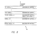
- This embodiment includes, for purposes of example, the embodiment of FIG. 2 , but with the addition of a fourth or bottom subcell 14. Accordingly, the third subcell 13 may be referred to as a lower or intermediate subcell.
- the fourth subcell 14 is shown with a fourth material system of Ge.
- the thicknesses of the subcells 11-14 are such that subcells 11-13 have the same photogenerated current density J ph (i.e., current matched condition), or substantially the same J ph .
- the fourth subcell 14 generates as much or more current than the first, second, and third subcells 11-13 as a result of its thickness and bandgap.
- a voltage of ⁇ 4.18 V is produced in this example, which is higher than the second embodiment described above.
- This 4-junction cell 10 shown in FIG. 3 would be expected to have a higher efficiency than the 3-junction cell 10 shown in FIG. 2 based on modeling calculations. The higher efficiency results from the additional voltage contributed by the fourth subcell 14. Additionally, the 4-junction cell 10 would be expected to have an efficiency within ⁇ 1% (absolute) of a conventional 3-junction GainP/GaAs/Ge cell with a single GaInP subcell based on modeling calculations.
- An additional example of this third embodiment is a GalnP/GalnP/GalnAs/Ge 4-junction cell 10.
- the basic combination of a thin GalnP subcell 11 and thick GaInP subcell 12 can further be used as the top two subcells of a 5-junction monolithic, series-interconnected photovoltaic cell.
- the third subcell 13 is made for example of GaAs
- the fourth subcell 14 is made for example of a semiconductor with a bandgap between that of GaAs and Ge (e.g., ⁇ 0.9 to 1.2 eV, GaInNAs lattice-matched to GaAs)
- a fifth or bottom subcell 15 made, for example, of Ge.
- the bandgap of subcell 14 is 1.05 eV.
- the thicknesses of the subcells are such that the first through fourth subcells 11-14 have the same photogenerated current density J ph (i.e., current matched condition), or substantially the same J ph .
- the fifth subcell 15 generates as much or more current that the first, second, third and fourth subcells 11-14.
- the 5-junction cell 10 would be expected to have an open-circuit voltage of ⁇ 4.8 V and to have a higher efficiency than the 4-junction cell in FIG. 3 , a conventional GalnP/GaAs/Ge 3-junction cell, or a conventional GalnP/GaAs/GalnNAs/Ge 4-junction cell.
- the advantage over the 4-junction cell 10 in FIG. 3 is largely due to the fourth subcell 14 in the 5-junction cell 10 providing a higher voltage than the fourth subcell 14 in the 4-junction cell 10.
- the advantage over the conventional GalnP/GaAs/GalnNAs/Ge 4-junction cell is largely due to the poor material quality and corresponding poor current production of the GaInNAs subcell.
- a variation of the 5-junction cell 10 shown in FIG. 4 would be a 4-junction GalnP/GalnP/GaAs/GalnNAs having a structure similar to the 5-junction cell but without a fifth subcell 15 (i.e., an inactive Ge or GaAs substrate in lieu of the fifth subcell 15).
- an important advantage of the 5-junction cell 10 shown in FIG. 4 is that, due to its low current and high voltage, the cell 10 can accommodate low current densities that are typically collected from the ⁇ 0.9 to 1.2 eV fourth subcell 14.
- GaInNAs solar cells lattice-matched to GaAs usually have collected current densities that are far below the photogenerated current density due to high electron-hole recombination.
- the current in each subcell 11-15 required for current matching is much lower than for a multijunction cell with a single GaInP subcell.
- GalnP/GaAs/GalnNAs/Ge 4-junction cell 10 assumes an optically thin GaAs subcell to allow enough incident light to reach the GaInNAs subcell for current matching. Note also that these modeled efficiencies are approximate. However, the set of assumptions used for the modeling calculations is consistent from case-to-case, allowing a valid comparison to be made between the various mulitjunction cell structures.
- GalnNAs subcells In order to achieve even about 60% of the maximum J ph , GalnNAs subcells (and perhaps other ⁇ 0.9 to 1.2 eV cells) must often rely on field-aided collection of carriers, rather than on carrier diffusion. In such subcells, almost all collection comes from the space-charge region (SCR) associated with the p-n junction.
- SCR space-charge region
- the base is lightly doped or compensated to make the SCR wider in order to collect more carriers within the SCR. But problems with doping control, as well as voltage drops and recombination in the SCR, make it advantageous to have a thinner SCR if possible.
- the low current requirements of the 5-junction cell 10 with a thin GalnP subcell 11/thick GaInP subcell 12 make it possible to achieve current matching with an SCR in the ⁇ 0.9 to 1.2 eV fourth subcell 14 of reasonable thickness and without excessive losses in voltage.
- the low current requirements of the 5-junction cell 10 with a thin GaInP subcell 11/thick GaInP subcell 12 may make it possible to use semiconductors with bandgaps that are slightly wider than would otherwise be possible in the ⁇ 0.9 to 1.2 eV fourth subcell 14.
- Increasing the bandgap of these materials may reduce the incidence of defects and, thus, result in greater carrier collection efficiencies.
- GaInNAs lattice-matched to GaAs has a lower nitrogen concentration at 1.15 eV than for 1.05 eV. If high nitrogen concentrations increase the density of the defects, then it may be easier to achieve current matching and higher efficiency if a 1.15 eV subcell with good carrier collection can be used.
- An example of such a 5-junction cell 10 is shown in FIG. 5 .
- a thin first subcell 11 a thicker second subcell 12 with the same composition of Ga 0.5 In 0.5 P, a GaAs third subcell 13, a ⁇ 0.9 to 1.2 eV fourth subcell 14 (e.g., GalnNAs), and a Ge fifth subcell 15 are provided.
- a 1.15 eV bandgap is used for the fourth subcell 14.
- the bandgap of subcell 11 can be increased, thus relaxing somewhat the need to make the subcell 11 very thin to allow current matching. This is shown in FIG. 6 .
- FIG. 6 depicts a sixth example not part of the present invention for another 5-junction cell 10, specifically, AlGalnP/GalnP/GaAs/GalnNAs/Ge.
- the AlGalnP first subcell 11 has a bandgap of 2.0 eV.
- the second GaInP subcell 12 has a bandgap of 1.80 eV, the third GaAs subcell 13 has a bandgap of 1.424 eV, the fourth subcell has a bandgap of ⁇ 0.9 to 1.2 eV, and the fifth subcell 15 has a bandgap of 0.66 eV.
- subcells 11, 12 are still considered to have similar compositions and similar bandgaps, much too close to allow current matching unless subcell 11 is made much thinner than subcell 12.
- the subcell 11 can be made slightly thicker than for a GalnP subcell 11, and the cell 10 efficiency is less sensitive to the exact thickness of the subcell 11.
- the fourth subcell 14 may be especially advantageous to thin the third GaAs subcell 13 to allow more light to reach the fourth subcell 14. Although this suppresses the current of the multijunction cell 10, it may be a net improvement in efficiency if this allows the fourth subcell 14 to be current matched to the rest of the subcells. An example of this case is illustrated in FIG.
- the fourth subcell 14 has a bandgap of 1.15 eV
- the third GaAs subcell 13 (as well as the first and second GaInP subcells 11, 12) have been thinned to give a maximum J ph of 11.48 mA/cm 2 , which is about 1 mA/cm 2 lower than the 12.44 mA/cm 2 of the previous example.
- the calculated efficiency in this case is 31.2%. This is lower than in the previous example, with 33.0% efficiency, for which the third GaAs subcell 13 did not have to be thinned, but is still higher than a conventional 3-junction cell.
- the fourth subcell 14 material is of poor electronic quality
- thinning the GaAs base may result in a higher multijunction cell efficiency by allowing current matching among the subcells.
- Widening the bandgap of the third subcell 13 by using GaInPAs lattice-matched to GaAs, instead of a third GaAs subcell 13, provides another way to allow more light to pass through the third subcell 13 to reach the poor current producing fourth subcell 14.
- the use of wider bandgap GaInPAs in the third subcell 13 can also increase the cell voltage.
- the thin GaInP subcell 11/thick GaInP subcell 12 is used in a structure similar to the 4-junction GalnP/GalnP/GaAs/Ge cell 10 shown in FIG.3 .
- the third GaAs subcell 13 is removed.
- the thicknesses of the subcells 11-13 are such that subcells 11, 12 have the same photogenerated current density (i.e., current matched condition), or nearly the same density, and the subcell 13 generates as much or more current than the other two subcells. This results in a 3-junction GalnP/GalnP/Ge cell 10 with a calculated efficiency of ⁇ 21.8%.
- the GalnP/GalnP/Ge 3-junction cell 10 has a thinner base in each GaInP subcell, particularly in the top subcell 11, and so may have greater radiation resistance in the GaInP subcells.
- the present invention provides a multijunction photovoltaic cell with improved radiation resistance.
- the photovoltaic cell of the invention combines the radiation resistance of GaInP with fairly narrow base thicknesses, which should reduce the susceptibility of minority carrier diffusion length to radiation degradation.
- the 2-junction GaInP/GaInP and 3-junction GaInP/GaInP/Ge cells of the present invention have no third GaAs subcell to degrade.
- the 3-junction GalnP/GalnP/GaAs cell has substantial excess current in the GaAs subcell, thereby making it fairly insensitive to degradation in the GaAs.
- the 5-junction GalnP/GaAs/GalnNAs/Ge and AlGalnP/GalnP/GaAs/GalnNAs/Ge cells have a thin GaAs subcell, while both the 4-junction GalnP/GalnP/GaAs/Ge and the 5-junction GalnP/GalnP/GaAs/GalnNAs/Ge cell may have a thin GaAs subcell. Reducing the thickness of the GaAs subcell decreases its sensitivity to minority carrier diffusion length, resulting in greater radiation resistance.
- the third through sixth embodiments have excess current in the Ge subcell, also increasing the radiation resistance.
- the thin subcell/thick subcell pair made out of the same or similar semiconductor material may be used for not only subcells 11 and 12, but may also be used for subcells 12 and 13, or subcells 13 and 14, or in general, for subcells j and j+1 in a multijunction cell 10 that has a total number of subcells n greater than or equal to j+1.
- This is equivalent to replacing a given subcell j in a given multijunction cell 10 having n subcells, with a thin subcell j and a thicker subcell j+1 made of the same or similar semiconductor composition, resulting in a multijunction cell 10 with a total of n+1 subcells.
- Examples of this embodiment are GalnP/GalnP/GaAs 3-junction cells, and GalnP/GaAs/GaAs/Ge 4-junction cells where the GaAs subcell 12 is thinner that the GaAs subcell 13, in order that the photogenerated current density is approximately the same for each of the GaAs subcells, in spite of the subcells 12 and 13 being composed of GaAs.
- GaInP/GaAs/Ge/Ge 4-junction cells GalnP/GaAs/GaAs/GalnNAs/Ge 5-junction cells
- GalnP/GalnAs/GalnAs/Ge 4-junction cells GalnP/GalnP/GaAs/GaAs/Ge 5-junction cells.
Claims (8)
- Cellule photovoltaïque multijonctions (10), caractérisée par :une première sous-cellule (11) fabriquée à partir d'un premier système de matériau, ayant une première bande interdite et produisant une première sortie de courant photogénérée ;une seconde sous-cellule (12) qui est disposée de façon immédiatement adjacente à ladite première sous-cellule (11), ladite seconde sous-cellule (12) étant fabriquée à partir d'un second système de matériau, ayant une seconde bande interdite inférieure à ladite première bande interdite et produisant une seconde sortie de courant photogénéré ; etune jonction à effet tunnel (16) disposée entre lesdites première et seconde sous-cellules (11, 12),caractérisée en ce queledit premier système de matériau est le même que ledit second système de matériau,lesdits premier et second systèmes de matériau sont Ga0.5In0,5P,ladite première sous-cellule (11) et ladite seconde sous-cellule (12) ont différents degrés de désordre de sous-réseau de groupe III donnant la différence entre lesdites première et seconde bandes interdites, etladite seconde sortie de courant photogénéré est sensiblement égale en quantité à ladite première sortie de courant photogénéré.
- Cellule selon la revendication 1, caractérisée en ce que ladite cellule (10) comprend une pluralité de sous-cellules (11, 12) dont le nombre total est au moins égal à deux.
- Cellule selon la revendication 1 ou 2, caractérisée en ce que ladite première sous-cellule (11) est disposée dans ladite cellule (10) de telle sorte que ladite première sous-cellule (11) est la première desdites sous-cellules (11, 12) à recevoir la lumière incidente sur ladite cellule (10).
- Cellule selon l'une quelconque des revendications précédentes, caractérisée en ce qu'une première épaisseur de ladite première sous-cellule (11) est inférieure à une seconde épaisseur de ladite seconde sous-cellule (12).
- Cellule selon l'une quelconque des revendications précédentes, caractérisée en ce que chacune desdites sous-cellules (11, 12) est l'une d'un type homojonction et d'un type hétérojonction.
- Cellule selon l'une quelconque des revendications précédentes, caractérisée en ce que chacune desdites sous-cellules (11, 12) comprend une base et un émetteur.
- Cellule selon la revendication 6, caractérisée en ce que chacune desdites sous-cellules (11, 12) comprend en outre une fenêtre opérationnellement adjacente audit émetteur.
- Cellule selon la revendication 6 ou 7, caractérisée en ce que chacune desdites sous-cellules (11, 12) comprend en outre une couche à champ électrique arrière opérationnellement adjacente à ladite base.
Applications Claiming Priority (2)
| Application Number | Priority Date | Filing Date | Title |
|---|---|---|---|
| US544834 | 2000-03-15 | ||
| US09/544,834 US6316715B1 (en) | 2000-03-15 | 2000-03-15 | Multijunction photovoltaic cell with thin 1st (top) subcell and thick 2nd subcell of same or similar semiconductor material |
Publications (3)
| Publication Number | Publication Date |
|---|---|
| EP1134813A2 EP1134813A2 (fr) | 2001-09-19 |
| EP1134813A3 EP1134813A3 (fr) | 2006-05-17 |
| EP1134813B1 true EP1134813B1 (fr) | 2011-06-08 |
Family
ID=24173777
Family Applications (1)
| Application Number | Title | Priority Date | Filing Date |
|---|---|---|---|
| EP01106191A Expired - Lifetime EP1134813B1 (fr) | 2000-03-15 | 2001-03-14 | Cellule photovoltaique multijonctions comportant une première cellule mince (supérieure) et une deuxième cellule plus épaisse du même matériau semiconducteur ou de matériau similaire |
Country Status (4)
| Country | Link |
|---|---|
| US (1) | US6316715B1 (fr) |
| EP (1) | EP1134813B1 (fr) |
| AT (1) | ATE512466T1 (fr) |
| CA (1) | CA2340997C (fr) |
Families Citing this family (80)
| Publication number | Priority date | Publication date | Assignee | Title |
|---|---|---|---|---|
| US6819845B2 (en) | 2001-08-02 | 2004-11-16 | Ultradots, Inc. | Optical devices with engineered nonlinear nanocomposite materials |
| US6710366B1 (en) | 2001-08-02 | 2004-03-23 | Ultradots, Inc. | Nanocomposite materials with engineered properties |
| US6794265B2 (en) | 2001-08-02 | 2004-09-21 | Ultradots, Inc. | Methods of forming quantum dots of Group IV semiconductor materials |
| US6660928B1 (en) | 2002-04-02 | 2003-12-09 | Essential Research, Inc. | Multi-junction photovoltaic cell |
| WO2003100868A1 (fr) * | 2002-05-21 | 2003-12-04 | Midwest Research Institute | Dispositifs optoelectroniques a bande interdite multiple, monolithiques et a faible bande interdite |
| US8173891B2 (en) * | 2002-05-21 | 2012-05-08 | Alliance For Sustainable Energy, Llc | Monolithic, multi-bandgap, tandem, ultra-thin, strain-counterbalanced, photovoltaic energy converters with optimal subcell bandgaps |
| US8067687B2 (en) | 2002-05-21 | 2011-11-29 | Alliance For Sustainable Energy, Llc | High-efficiency, monolithic, multi-bandgap, tandem photovoltaic energy converters |
| US20060162768A1 (en) | 2002-05-21 | 2006-07-27 | Wanlass Mark W | Low bandgap, monolithic, multi-bandgap, optoelectronic devices |
| US7217882B2 (en) * | 2002-05-24 | 2007-05-15 | Cornell Research Foundation, Inc. | Broad spectrum solar cell |
| US7126052B2 (en) * | 2002-10-02 | 2006-10-24 | The Boeing Company | Isoelectronic surfactant induced sublattice disordering in optoelectronic devices |
| US7122734B2 (en) * | 2002-10-23 | 2006-10-17 | The Boeing Company | Isoelectronic surfactant suppression of threading dislocations in metamorphic epitaxial layers |
| US7071407B2 (en) * | 2002-10-31 | 2006-07-04 | Emcore Corporation | Method and apparatus of multiplejunction solar cell structure with high band gap heterojunction middle cell |
| WO2004054003A1 (fr) * | 2002-12-05 | 2004-06-24 | Blue Photonics, Inc. | Piles solaires multijonctions, monolithiques, a efficacite elevee, contenant des materiaux a reseaux non apparies et procedes de formation associes |
| JP2004296658A (ja) * | 2003-03-26 | 2004-10-21 | Sharp Corp | 多接合太陽電池およびその電流整合方法 |
| US7812249B2 (en) * | 2003-04-14 | 2010-10-12 | The Boeing Company | Multijunction photovoltaic cell grown on high-miscut-angle substrate |
| US7488890B2 (en) * | 2003-04-21 | 2009-02-10 | Sharp Kabushiki Kaisha | Compound solar battery and manufacturing method thereof |
| US7807921B2 (en) * | 2004-06-15 | 2010-10-05 | The Boeing Company | Multijunction solar cell having a lattice mismatched GrIII-GrV-X layer and a composition-graded buffer layer |
| US8227689B2 (en) | 2004-06-15 | 2012-07-24 | The Boeing Company | Solar cells having a transparent composition-graded buffer layer |
| US20060048811A1 (en) * | 2004-09-09 | 2006-03-09 | Krut Dimitri D | Multijunction laser power converter |
| US8772628B2 (en) | 2004-12-30 | 2014-07-08 | Alliance For Sustainable Energy, Llc | High performance, high bandgap, lattice-mismatched, GaInP solar cells |
| US10069026B2 (en) * | 2005-12-19 | 2018-09-04 | The Boeing Company | Reduced band gap absorber for solar cells |
| US10381505B2 (en) | 2007-09-24 | 2019-08-13 | Solaero Technologies Corp. | Inverted metamorphic multijunction solar cells including metamorphic layers |
| US8916769B2 (en) | 2008-10-01 | 2014-12-23 | International Business Machines Corporation | Tandem nanofilm interconnected semiconductor wafer solar cells |
| US8912428B2 (en) * | 2008-10-22 | 2014-12-16 | Epir Technologies, Inc. | High efficiency multijunction II-VI photovoltaic solar cells |
| TWI427806B (zh) | 2009-01-12 | 2014-02-21 | Epistar Corp | 堆疊型太陽能電池 |
| KR20100084843A (ko) * | 2009-01-19 | 2010-07-28 | 삼성전자주식회사 | 다중접합 태양전지 |
| US9722131B2 (en) * | 2009-03-16 | 2017-08-01 | The Boeing Company | Highly doped layer for tunnel junctions in solar cells |
| US8609984B2 (en) * | 2009-06-24 | 2013-12-17 | Florida State University Research Foundation, Inc. | High efficiency photovoltaic cell for solar energy harvesting |
| TWI409959B (zh) * | 2009-12-07 | 2013-09-21 | Epistar Corp | 太陽能電池元件及其裝置 |
| CN103354250B (zh) * | 2010-03-19 | 2016-03-02 | 晶元光电股份有限公司 | 一种具有渐变缓冲层太阳能电池 |
| EP2628183A4 (fr) | 2010-10-12 | 2014-04-02 | Alliance Sustainable Energy | Alliages iii-v à bande interdite importante pour composants optoélectroniques de grande efficacité |
| US11417788B2 (en) | 2010-11-19 | 2022-08-16 | The Boeing Company | Type-II high bandgap tunnel junctions of InP lattice constant for multijunction solar cells |
| US8604330B1 (en) | 2010-12-06 | 2013-12-10 | 4Power, Llc | High-efficiency solar-cell arrays with integrated devices and methods for forming them |
| US9818901B2 (en) * | 2011-05-13 | 2017-11-14 | International Business Machines Corporation | Wafer bonded solar cells and fabrication methods |
| US8073645B2 (en) * | 2011-05-30 | 2011-12-06 | Cyrium Technologies Incorporated | Apparatus and method to characterize multijunction photovoltaic solar cells |
| CN102244114A (zh) * | 2011-06-22 | 2011-11-16 | 厦门市三安光电科技有限公司 | 一种高倍聚光多结太阳能电池及其制备方法 |
| US20130048061A1 (en) * | 2011-08-24 | 2013-02-28 | International Business Machines Corporation | Monolithic multi-junction photovoltaic cell and method |
| FR2981195A1 (fr) * | 2011-10-11 | 2013-04-12 | Soitec Silicon On Insulator | Multi-jonctions dans un dispositif semi-conducteur forme par differentes techniques de depot |
| US8624222B2 (en) | 2011-10-21 | 2014-01-07 | University Of Utah Research Foundation | Homogeneous multiple band gap devices |
| CN102790116B (zh) * | 2012-07-19 | 2015-09-09 | 中国科学院苏州纳米技术与纳米仿生研究所 | 倒装GaInP/GaAs/Ge/Ge四结太阳能电池及其制备方法 |
| CN102790119B (zh) * | 2012-07-19 | 2015-12-16 | 中国科学院苏州纳米技术与纳米仿生研究所 | GaInP/GaAs/Ge/Ge四结太阳能电池及其制备方法 |
| CN102790121B (zh) * | 2012-08-09 | 2015-12-16 | 厦门大学 | 具有两结锗子电池的四结太阳能电池及其制备方法 |
| US11495705B2 (en) | 2012-09-14 | 2022-11-08 | The Boeing Company | Group-IV solar cell structure using group-IV or III-V heterostructures |
| US9099595B2 (en) | 2012-09-14 | 2015-08-04 | The Boeing Company | Group-IV solar cell structure using group-IV or III-V heterostructures |
| US10903383B2 (en) | 2012-09-14 | 2021-01-26 | The Boeing Company | Group-IV solar cell structure using group-IV or III-V heterostructures |
| US9985160B2 (en) | 2012-09-14 | 2018-05-29 | The Boeing Company | Group-IV solar cell structure using group-IV or III-V heterostructures |
| US9997659B2 (en) | 2012-09-14 | 2018-06-12 | The Boeing Company | Group-IV solar cell structure using group-IV or III-V heterostructures |
| US11646388B2 (en) | 2012-09-14 | 2023-05-09 | The Boeing Company | Group-IV solar cell structure using group-IV or III-V heterostructures |
| US20140150856A1 (en) * | 2012-11-30 | 2014-06-05 | Intellectual Discovery Co., Ltd. | Photovoltaic module |
| KR20140082012A (ko) * | 2012-12-21 | 2014-07-02 | 엘지전자 주식회사 | 태양 전지 및 이의 제조 방법 |
| US8580658B1 (en) | 2012-12-21 | 2013-11-12 | Solan, LLC | Methods for fabricating graphene device topography and devices formed therefrom |
| TWI602315B (zh) * | 2013-03-08 | 2017-10-11 | 索泰克公司 | 具有經組構成效能更佳之低帶隙主動層之感光元件及相關方法 |
| US8853061B1 (en) | 2013-03-15 | 2014-10-07 | Solan, LLC | Methods for manufacturing nonplanar graphite-based devices having multiple bandgaps |
| US9590131B2 (en) | 2013-03-27 | 2017-03-07 | Alliance For Sustainable Energy, Llc | Systems and methods for advanced ultra-high-performance InP solar cells |
| DE102015006379B4 (de) * | 2015-05-18 | 2022-03-17 | Azur Space Solar Power Gmbh | Skalierbare Spannungsquelle |
| US9899550B2 (en) | 2015-08-12 | 2018-02-20 | Toyota Motor Engineering & Manufacturing North America, Inc. | Electric power transfer system using optical power transfer |
| US11563133B1 (en) | 2015-08-17 | 2023-01-24 | SolAero Techologies Corp. | Method of fabricating multijunction solar cells for space applications |
| DE102015013514B4 (de) * | 2015-10-20 | 2024-04-18 | Azur Space Solar Power Gmbh | Optischer Empfängerbaustein |
| DE102015016047A1 (de) * | 2015-12-10 | 2017-06-14 | Azur Space Solar Power Gmbh | Mehrfach-Solarzelle |
| DE102015016822B4 (de) * | 2015-12-25 | 2023-01-05 | Azur Space Solar Power Gmbh | Stapelförmige Mehrfach-Solarzelle |
| DE102016001386A1 (de) * | 2016-02-09 | 2017-08-10 | Azur Space Solar Power Gmbh | Stapelförmige Mehrfachsolarzelle |
| DE102016001387A1 (de) * | 2016-02-09 | 2017-08-10 | Azur Space Solar Power Gmbh | Empfängerbaustein |
| US10700230B1 (en) | 2016-10-14 | 2020-06-30 | Solaero Technologies Corp. | Multijunction metamorphic solar cell for space applications |
| DE102016013749A1 (de) * | 2016-11-18 | 2018-05-24 | Azur Space Solar Power Gmbh | Stapelförmige Halbleiterstruktur |
| TR201700484A2 (tr) * | 2017-01-12 | 2017-10-23 | Hat Teknoloji A S | Güneş işiğindan elektri̇k üretmek i̇çi̇n bi̇r solar hücre ve solar panel |
| DE102017200700A1 (de) * | 2017-01-18 | 2018-07-19 | Fraunhofer-Gesellschaft zur Förderung der angewandten Forschung e.V. | Mehrfachsolarzelle mit rückseitiger Germanium-Teilzelle und deren Verwendung |
| US11527667B2 (en) * | 2017-04-27 | 2022-12-13 | Alliance For Sustainable Energy, Llc | Tunnel junctions for multijunction solar cells |
| US11264524B1 (en) * | 2018-02-08 | 2022-03-01 | Solaero Technologies Corp. | Multijunction solar cells |
| RU2671549C1 (ru) * | 2018-02-09 | 2018-11-01 | Российская Федерация, от имени которой выступает Государственная корпорация по космической деятельности "РОСКОСМОС" | Фотоэлектрический преобразователь с просветляющим нанопокрытием |
| DE102018001592A1 (de) * | 2018-03-01 | 2019-09-05 | Azur Space Solar Power Gmbh | Mehrfachsolarzelle |
| DE102018009744A1 (de) * | 2018-12-14 | 2020-06-18 | Azur Space Solar Power Gmbh | Stapelförmige monolithische aufrecht-metamorphe Mehrfachsolarzelle |
| DE102018009850A1 (de) * | 2018-12-19 | 2020-06-25 | Azur Space Solar Power Gmbh | Stapelförmige Mehrfachsolarzelle |
| US11563137B2 (en) | 2019-09-16 | 2023-01-24 | Meta Platforms Technologies, Llc | Optical transformer |
| EP3799136B1 (fr) * | 2019-09-27 | 2023-02-01 | AZUR SPACE Solar Power GmbH | Cellule solaire monolithique à multi-jonctions comportant exactement quatre sous-cellules |
| US11658256B2 (en) | 2019-12-16 | 2023-05-23 | Solaero Technologies Corp. | Multijunction solar cells |
| US11978813B1 (en) * | 2019-12-23 | 2024-05-07 | United States Of America As Represented By The Secretary Of The Air Force | Systems, methods and apparatus for coupling solar cells |
| EP3937259A1 (fr) * | 2020-07-10 | 2022-01-12 | AZUR SPACE Solar Power GmbH | Cellule solaire multiple métamorphique monolithique |
| US11431236B2 (en) | 2020-08-18 | 2022-08-30 | Meta Platforms Technologies, Llc | Dynamically addressable high voltage optical transformer with integrated optically triggered switches |
| EP3965168B1 (fr) * | 2020-09-07 | 2023-03-08 | AZUR SPACE Solar Power GmbH | Cellule solaire multiple monolithique empilée |
| US11362230B1 (en) | 2021-01-28 | 2022-06-14 | Solaero Technologies Corp. | Multijunction solar cells |
Family Cites Families (15)
| Publication number | Priority date | Publication date | Assignee | Title |
|---|---|---|---|---|
| US4017332A (en) | 1975-02-27 | 1977-04-12 | Varian Associates | Solar cells employing stacked opposite conductivity layers |
| US4127862A (en) * | 1977-09-06 | 1978-11-28 | Bell Telephone Laboratories, Incorporated | Integrated optical detectors |
| US4332974A (en) | 1979-06-28 | 1982-06-01 | Chevron Research Company | Multilayer photovoltaic cell |
| US4255211A (en) | 1979-12-31 | 1981-03-10 | Chevron Research Company | Multilayer photovoltaic solar cell with semiconductor layer at shorting junction interface |
| US4377723A (en) * | 1980-05-02 | 1983-03-22 | The University Of Delaware | High efficiency thin-film multiple-gap photovoltaic device |
| US4688068A (en) * | 1983-07-08 | 1987-08-18 | The United States Of America As Represented By The Department Of Energy | Quantum well multijunction photovoltaic cell |
| US4631352A (en) * | 1985-12-17 | 1986-12-23 | The United States Of America As Represented By The Administrator Of The National Aeronautics And Space Administration | High band gap II-VI and III-V tunneling junctions for silicon multijunction solar cells |
| JPS62234379A (ja) * | 1986-04-04 | 1987-10-14 | Kanegafuchi Chem Ind Co Ltd | 半導体装置 |
| JPH0795602B2 (ja) | 1989-12-01 | 1995-10-11 | 三菱電機株式会社 | 太陽電池及びその製造方法 |
| US5223043A (en) * | 1991-02-11 | 1993-06-29 | The United States Of America As Represented By The United States Department Of Energy | Current-matched high-efficiency, multijunction monolithic solar cells |
| US5322573A (en) | 1992-10-02 | 1994-06-21 | The United States Of America As Represented By The Administrator Of The National Aeronautics And Space Administration | InP solar cell with window layer |
| US5407491A (en) | 1993-04-08 | 1995-04-18 | University Of Houston | Tandem solar cell with improved tunnel junction |
| US5800630A (en) | 1993-04-08 | 1998-09-01 | University Of Houston | Tandem solar cell with indium phosphide tunnel junction |
| US5716480A (en) * | 1995-07-13 | 1998-02-10 | Canon Kabushiki Kaisha | Photovoltaic device and method of manufacturing the same |
| US5853497A (en) * | 1996-12-12 | 1998-12-29 | Hughes Electronics Corporation | High efficiency multi-junction solar cells |
-
2000
- 2000-03-15 US US09/544,834 patent/US6316715B1/en not_active Expired - Lifetime
-
2001
- 2001-03-14 EP EP01106191A patent/EP1134813B1/fr not_active Expired - Lifetime
- 2001-03-14 CA CA002340997A patent/CA2340997C/fr not_active Expired - Lifetime
- 2001-03-14 AT AT01106191T patent/ATE512466T1/de not_active IP Right Cessation
Also Published As
| Publication number | Publication date |
|---|---|
| US6316715B1 (en) | 2001-11-13 |
| ATE512466T1 (de) | 2011-06-15 |
| EP1134813A3 (fr) | 2006-05-17 |
| CA2340997A1 (fr) | 2001-09-15 |
| CA2340997C (fr) | 2004-02-17 |
| EP1134813A2 (fr) | 2001-09-19 |
Similar Documents
| Publication | Publication Date | Title |
|---|---|---|
| EP1134813B1 (fr) | Cellule photovoltaique multijonctions comportant une première cellule mince (supérieure) et une deuxième cellule plus épaisse du même matériau semiconducteur ou de matériau similaire | |
| US11411129B2 (en) | Solar cells having a transparent composition-graded buffer layer | |
| US6150603A (en) | Bilayer passivation structure for photovoltaic cells | |
| EP1469528B1 (fr) | CELLULE PHOTOVOLTAïQUE À TRIPLE JONCTION CRÛE SUR UN SUBSTRAT COUPÉ À GRAND ANGLE | |
| US8912428B2 (en) | High efficiency multijunction II-VI photovoltaic solar cells | |
| US6340788B1 (en) | Multijunction photovoltaic cells and panels using a silicon or silicon-germanium active substrate cell for space and terrestrial applications | |
| US7807921B2 (en) | Multijunction solar cell having a lattice mismatched GrIII-GrV-X layer and a composition-graded buffer layer | |
| TWI600173B (zh) | 在中間電池中具有低能隙吸收層之多接面太陽能電池及其製造方法 | |
| KR101908742B1 (ko) | 다중접합 태양전지를 위한 인화인듐 격자 상수의 타입-2 고 밴드갭 터널 접합 | |
| Dimroth et al. | Metamorphic GayIn1− yP/Ga1− xInxAs tandem solar cells for space and for terrestrial concentrator applications at C> 1000 suns | |
| US20090188561A1 (en) | High concentration terrestrial solar array with III-V compound semiconductor cell | |
| US20090188554A1 (en) | III-V Compound Semiconductor Solar Cell for Terrestrial Solar Array | |
| Dimroth et al. | 3-6 junction photovoltaic cells for space and terrestrial concentrator applications | |
| EP4036992A1 (fr) | Cellule solaire à quatre jonctions et ensembles pile solaire pour applications spatiales | |
| US10861992B2 (en) | Perovskite solar cells for space | |
| Yuen et al. | High efficiency solar cells at solar junction | |
| Andreev | Application of III–V compounds in solar cells |
Legal Events
| Date | Code | Title | Description |
|---|---|---|---|
| PUAI | Public reference made under article 153(3) epc to a published international application that has entered the european phase |
Free format text: ORIGINAL CODE: 0009012 |
|
| AK | Designated contracting states |
Kind code of ref document: A2 Designated state(s): AT BE CH CY DE DK ES FI FR GB GR IE IT LI LU MC NL PT SE TR |
|
| AX | Request for extension of the european patent |
Free format text: AL;LT;LV;MK;RO;SI |
|
| PUAL | Search report despatched |
Free format text: ORIGINAL CODE: 0009013 |
|
| AK | Designated contracting states |
Kind code of ref document: A3 Designated state(s): AT BE CH CY DE DK ES FI FR GB GR IE IT LI LU MC NL PT SE TR |
|
| AX | Request for extension of the european patent |
Extension state: AL LT LV MK RO SI |
|
| 17P | Request for examination filed |
Effective date: 20061115 |
|
| AKX | Designation fees paid |
Designated state(s): AT BE CH CY DE DK ES FI FR GB GR IE IT LI LU MC NL PT SE TR |
|
| 17Q | First examination report despatched |
Effective date: 20071121 |
|
| GRAP | Despatch of communication of intention to grant a patent |
Free format text: ORIGINAL CODE: EPIDOSNIGR1 |
|
| GRAS | Grant fee paid |
Free format text: ORIGINAL CODE: EPIDOSNIGR3 |
|
| GRAA | (expected) grant |
Free format text: ORIGINAL CODE: 0009210 |
|
| AK | Designated contracting states |
Kind code of ref document: B1 Designated state(s): AT BE CH CY DE DK ES FI FR GB GR IE IT LI LU MC NL PT SE TR |
|
| REG | Reference to a national code |
Ref country code: GB Ref legal event code: FG4D |
|
| REG | Reference to a national code |
Ref country code: CH Ref legal event code: EP |
|
| REG | Reference to a national code |
Ref country code: IE Ref legal event code: FG4D |
|
| REG | Reference to a national code |
Ref country code: DE Ref legal event code: R096 Ref document number: 60144738 Country of ref document: DE Effective date: 20110721 |
|
| REG | Reference to a national code |
Ref country code: NL Ref legal event code: VDEP Effective date: 20110608 |
|
| PG25 | Lapsed in a contracting state [announced via postgrant information from national office to epo] |
Ref country code: SE Free format text: LAPSE BECAUSE OF FAILURE TO SUBMIT A TRANSLATION OF THE DESCRIPTION OR TO PAY THE FEE WITHIN THE PRESCRIBED TIME-LIMIT Effective date: 20110608 |
|
| PG25 | Lapsed in a contracting state [announced via postgrant information from national office to epo] |
Ref country code: FI Free format text: LAPSE BECAUSE OF FAILURE TO SUBMIT A TRANSLATION OF THE DESCRIPTION OR TO PAY THE FEE WITHIN THE PRESCRIBED TIME-LIMIT Effective date: 20110608 Ref country code: GR Free format text: LAPSE BECAUSE OF FAILURE TO SUBMIT A TRANSLATION OF THE DESCRIPTION OR TO PAY THE FEE WITHIN THE PRESCRIBED TIME-LIMIT Effective date: 20110909 Ref country code: ES Free format text: LAPSE BECAUSE OF FAILURE TO SUBMIT A TRANSLATION OF THE DESCRIPTION OR TO PAY THE FEE WITHIN THE PRESCRIBED TIME-LIMIT Effective date: 20110919 Ref country code: CY Free format text: LAPSE BECAUSE OF FAILURE TO SUBMIT A TRANSLATION OF THE DESCRIPTION OR TO PAY THE FEE WITHIN THE PRESCRIBED TIME-LIMIT Effective date: 20110608 Ref country code: AT Free format text: LAPSE BECAUSE OF FAILURE TO SUBMIT A TRANSLATION OF THE DESCRIPTION OR TO PAY THE FEE WITHIN THE PRESCRIBED TIME-LIMIT Effective date: 20110608 |
|
| PG25 | Lapsed in a contracting state [announced via postgrant information from national office to epo] |
Ref country code: BE Free format text: LAPSE BECAUSE OF FAILURE TO SUBMIT A TRANSLATION OF THE DESCRIPTION OR TO PAY THE FEE WITHIN THE PRESCRIBED TIME-LIMIT Effective date: 20110608 Ref country code: NL Free format text: LAPSE BECAUSE OF FAILURE TO SUBMIT A TRANSLATION OF THE DESCRIPTION OR TO PAY THE FEE WITHIN THE PRESCRIBED TIME-LIMIT Effective date: 20110608 |
|
| PG25 | Lapsed in a contracting state [announced via postgrant information from national office to epo] |
Ref country code: PT Free format text: LAPSE BECAUSE OF FAILURE TO SUBMIT A TRANSLATION OF THE DESCRIPTION OR TO PAY THE FEE WITHIN THE PRESCRIBED TIME-LIMIT Effective date: 20111010 |
|
| PLBE | No opposition filed within time limit |
Free format text: ORIGINAL CODE: 0009261 |
|
| STAA | Information on the status of an ep patent application or granted ep patent |
Free format text: STATUS: NO OPPOSITION FILED WITHIN TIME LIMIT |
|
| 26N | No opposition filed |
Effective date: 20120309 |
|
| PG25 | Lapsed in a contracting state [announced via postgrant information from national office to epo] |
Ref country code: IT Free format text: LAPSE BECAUSE OF FAILURE TO SUBMIT A TRANSLATION OF THE DESCRIPTION OR TO PAY THE FEE WITHIN THE PRESCRIBED TIME-LIMIT Effective date: 20110608 |
|
| PG25 | Lapsed in a contracting state [announced via postgrant information from national office to epo] |
Ref country code: DK Free format text: LAPSE BECAUSE OF FAILURE TO SUBMIT A TRANSLATION OF THE DESCRIPTION OR TO PAY THE FEE WITHIN THE PRESCRIBED TIME-LIMIT Effective date: 20110608 |
|
| REG | Reference to a national code |
Ref country code: DE Ref legal event code: R097 Ref document number: 60144738 Country of ref document: DE Effective date: 20120309 |
|
| PG25 | Lapsed in a contracting state [announced via postgrant information from national office to epo] |
Ref country code: MC Free format text: LAPSE BECAUSE OF NON-PAYMENT OF DUE FEES Effective date: 20120331 |
|
| REG | Reference to a national code |
Ref country code: CH Ref legal event code: PL |
|
| REG | Reference to a national code |
Ref country code: IE Ref legal event code: MM4A |
|
| PG25 | Lapsed in a contracting state [announced via postgrant information from national office to epo] |
Ref country code: LI Free format text: LAPSE BECAUSE OF NON-PAYMENT OF DUE FEES Effective date: 20120331 Ref country code: CH Free format text: LAPSE BECAUSE OF NON-PAYMENT OF DUE FEES Effective date: 20120331 Ref country code: IE Free format text: LAPSE BECAUSE OF NON-PAYMENT OF DUE FEES Effective date: 20120314 |
|
| PG25 | Lapsed in a contracting state [announced via postgrant information from national office to epo] |
Ref country code: TR Free format text: LAPSE BECAUSE OF FAILURE TO SUBMIT A TRANSLATION OF THE DESCRIPTION OR TO PAY THE FEE WITHIN THE PRESCRIBED TIME-LIMIT Effective date: 20110608 |
|
| PG25 | Lapsed in a contracting state [announced via postgrant information from national office to epo] |
Ref country code: LU Free format text: LAPSE BECAUSE OF NON-PAYMENT OF DUE FEES Effective date: 20120314 |
|
| REG | Reference to a national code |
Ref country code: FR Ref legal event code: PLFP Year of fee payment: 16 |
|
| REG | Reference to a national code |
Ref country code: FR Ref legal event code: PLFP Year of fee payment: 17 |
|
| REG | Reference to a national code |
Ref country code: FR Ref legal event code: PLFP Year of fee payment: 18 |
|
| PGFP | Annual fee paid to national office [announced via postgrant information from national office to epo] |
Ref country code: DE Payment date: 20200327 Year of fee payment: 20 Ref country code: GB Payment date: 20200327 Year of fee payment: 20 |
|
| PGFP | Annual fee paid to national office [announced via postgrant information from national office to epo] |
Ref country code: FR Payment date: 20200325 Year of fee payment: 20 |
|
| REG | Reference to a national code |
Ref country code: DE Ref legal event code: R071 Ref document number: 60144738 Country of ref document: DE |
|
| REG | Reference to a national code |
Ref country code: GB Ref legal event code: PE20 Expiry date: 20210313 |
|
| PG25 | Lapsed in a contracting state [announced via postgrant information from national office to epo] |
Ref country code: GB Free format text: LAPSE BECAUSE OF EXPIRATION OF PROTECTION Effective date: 20210313 |