EP1134806A2 - Stress reducing lead-frame for plastic encapsulation - Google Patents
Stress reducing lead-frame for plastic encapsulation Download PDFInfo
- Publication number
- EP1134806A2 EP1134806A2 EP01103220A EP01103220A EP1134806A2 EP 1134806 A2 EP1134806 A2 EP 1134806A2 EP 01103220 A EP01103220 A EP 01103220A EP 01103220 A EP01103220 A EP 01103220A EP 1134806 A2 EP1134806 A2 EP 1134806A2
- Authority
- EP
- European Patent Office
- Prior art keywords
- integrated circuit
- die
- circuit die
- mounting structure
- spreader
- Prior art date
- Legal status (The legal status is an assumption and is not a legal conclusion. Google has not performed a legal analysis and makes no representation as to the accuracy of the status listed.)
- Withdrawn
Links
Images



Classifications
-
- H—ELECTRICITY
- H10—SEMICONDUCTOR DEVICES; ELECTRIC SOLID-STATE DEVICES NOT OTHERWISE PROVIDED FOR
- H10W—GENERIC PACKAGES, INTERCONNECTIONS, CONNECTORS OR OTHER CONSTRUCTIONAL DETAILS OF DEVICES COVERED BY CLASS H10
- H10W70/00—Package substrates; Interposers; Redistribution layers [RDL]
- H10W70/40—Leadframes
- H10W70/411—Chip-supporting parts, e.g. die pads
- H10W70/417—Bonding materials between chips and die pads
-
- H—ELECTRICITY
- H10—SEMICONDUCTOR DEVICES; ELECTRIC SOLID-STATE DEVICES NOT OTHERWISE PROVIDED FOR
- H10W—GENERIC PACKAGES, INTERCONNECTIONS, CONNECTORS OR OTHER CONSTRUCTIONAL DETAILS OF DEVICES COVERED BY CLASS H10
- H10W72/00—Interconnections or connectors in packages
- H10W72/071—Connecting or disconnecting
-
- H—ELECTRICITY
- H10—SEMICONDUCTOR DEVICES; ELECTRIC SOLID-STATE DEVICES NOT OTHERWISE PROVIDED FOR
- H10W—GENERIC PACKAGES, INTERCONNECTIONS, CONNECTORS OR OTHER CONSTRUCTIONAL DETAILS OF DEVICES COVERED BY CLASS H10
- H10W70/00—Package substrates; Interposers; Redistribution layers [RDL]
- H10W70/40—Leadframes
- H10W70/421—Shapes or dispositions
- H10W70/424—Cross-sectional shapes
-
- H—ELECTRICITY
- H10—SEMICONDUCTOR DEVICES; ELECTRIC SOLID-STATE DEVICES NOT OTHERWISE PROVIDED FOR
- H10W—GENERIC PACKAGES, INTERCONNECTIONS, CONNECTORS OR OTHER CONSTRUCTIONAL DETAILS OF DEVICES COVERED BY CLASS H10
- H10W70/00—Package substrates; Interposers; Redistribution layers [RDL]
- H10W70/40—Leadframes
- H10W70/421—Shapes or dispositions
- H10W70/433—Shapes or dispositions of deformation-absorbing parts, e.g. leads having meandering shapes
-
- H—ELECTRICITY
- H10—SEMICONDUCTOR DEVICES; ELECTRIC SOLID-STATE DEVICES NOT OTHERWISE PROVIDED FOR
- H10W—GENERIC PACKAGES, INTERCONNECTIONS, CONNECTORS OR OTHER CONSTRUCTIONAL DETAILS OF DEVICES COVERED BY CLASS H10
- H10W72/00—Interconnections or connectors in packages
- H10W72/071—Connecting or disconnecting
- H10W72/073—Connecting or disconnecting of die-attach connectors
-
- H—ELECTRICITY
- H10—SEMICONDUCTOR DEVICES; ELECTRIC SOLID-STATE DEVICES NOT OTHERWISE PROVIDED FOR
- H10W—GENERIC PACKAGES, INTERCONNECTIONS, CONNECTORS OR OTHER CONSTRUCTIONAL DETAILS OF DEVICES COVERED BY CLASS H10
- H10W72/00—Interconnections or connectors in packages
- H10W72/071—Connecting or disconnecting
- H10W72/073—Connecting or disconnecting of die-attach connectors
- H10W72/07321—Aligning
- H10W72/07327—Aligning involving guiding structures, e.g. spacers or supporting members
-
- H—ELECTRICITY
- H10—SEMICONDUCTOR DEVICES; ELECTRIC SOLID-STATE DEVICES NOT OTHERWISE PROVIDED FOR
- H10W—GENERIC PACKAGES, INTERCONNECTIONS, CONNECTORS OR OTHER CONSTRUCTIONAL DETAILS OF DEVICES COVERED BY CLASS H10
- H10W72/00—Interconnections or connectors in packages
- H10W72/071—Connecting or disconnecting
- H10W72/073—Connecting or disconnecting of die-attach connectors
- H10W72/07331—Connecting techniques
- H10W72/07337—Connecting techniques using a polymer adhesive, e.g. an adhesive based on silicone or epoxy
-
- H—ELECTRICITY
- H10—SEMICONDUCTOR DEVICES; ELECTRIC SOLID-STATE DEVICES NOT OTHERWISE PROVIDED FOR
- H10W—GENERIC PACKAGES, INTERCONNECTIONS, CONNECTORS OR OTHER CONSTRUCTIONAL DETAILS OF DEVICES COVERED BY CLASS H10
- H10W72/00—Interconnections or connectors in packages
- H10W72/071—Connecting or disconnecting
- H10W72/073—Connecting or disconnecting of die-attach connectors
- H10W72/07351—Connecting or disconnecting of die-attach connectors characterised by changes in properties of the die-attach connectors during connecting
- H10W72/07352—Connecting or disconnecting of die-attach connectors characterised by changes in properties of the die-attach connectors during connecting changes in structures or sizes
-
- H—ELECTRICITY
- H10—SEMICONDUCTOR DEVICES; ELECTRIC SOLID-STATE DEVICES NOT OTHERWISE PROVIDED FOR
- H10W—GENERIC PACKAGES, INTERCONNECTIONS, CONNECTORS OR OTHER CONSTRUCTIONAL DETAILS OF DEVICES COVERED BY CLASS H10
- H10W72/00—Interconnections or connectors in packages
- H10W72/071—Connecting or disconnecting
- H10W72/073—Connecting or disconnecting of die-attach connectors
- H10W72/07351—Connecting or disconnecting of die-attach connectors characterised by changes in properties of the die-attach connectors during connecting
- H10W72/07353—Connecting or disconnecting of die-attach connectors characterised by changes in properties of the die-attach connectors during connecting changes in shapes
-
- H—ELECTRICITY
- H10—SEMICONDUCTOR DEVICES; ELECTRIC SOLID-STATE DEVICES NOT OTHERWISE PROVIDED FOR
- H10W—GENERIC PACKAGES, INTERCONNECTIONS, CONNECTORS OR OTHER CONSTRUCTIONAL DETAILS OF DEVICES COVERED BY CLASS H10
- H10W72/00—Interconnections or connectors in packages
- H10W72/30—Die-attach connectors
- H10W72/321—Structures or relative sizes of die-attach connectors
-
- H—ELECTRICITY
- H10—SEMICONDUCTOR DEVICES; ELECTRIC SOLID-STATE DEVICES NOT OTHERWISE PROVIDED FOR
- H10W—GENERIC PACKAGES, INTERCONNECTIONS, CONNECTORS OR OTHER CONSTRUCTIONAL DETAILS OF DEVICES COVERED BY CLASS H10
- H10W72/00—Interconnections or connectors in packages
- H10W72/30—Die-attach connectors
- H10W72/331—Shapes of die-attach connectors
- H10W72/334—Cross-sectional shape, i.e. in side view
-
- H—ELECTRICITY
- H10—SEMICONDUCTOR DEVICES; ELECTRIC SOLID-STATE DEVICES NOT OTHERWISE PROVIDED FOR
- H10W—GENERIC PACKAGES, INTERCONNECTIONS, CONNECTORS OR OTHER CONSTRUCTIONAL DETAILS OF DEVICES COVERED BY CLASS H10
- H10W72/00—Interconnections or connectors in packages
- H10W72/30—Die-attach connectors
- H10W72/351—Materials of die-attach connectors
- H10W72/353—Materials of die-attach connectors not comprising solid metals or solid metalloids, e.g. ceramics
- H10W72/354—Materials of die-attach connectors not comprising solid metals or solid metalloids, e.g. ceramics comprising polymers
-
- H—ELECTRICITY
- H10—SEMICONDUCTOR DEVICES; ELECTRIC SOLID-STATE DEVICES NOT OTHERWISE PROVIDED FOR
- H10W—GENERIC PACKAGES, INTERCONNECTIONS, CONNECTORS OR OTHER CONSTRUCTIONAL DETAILS OF DEVICES COVERED BY CLASS H10
- H10W72/00—Interconnections or connectors in packages
- H10W72/90—Bond pads, in general
- H10W72/931—Shapes of bond pads
-
- H—ELECTRICITY
- H10—SEMICONDUCTOR DEVICES; ELECTRIC SOLID-STATE DEVICES NOT OTHERWISE PROVIDED FOR
- H10W—GENERIC PACKAGES, INTERCONNECTIONS, CONNECTORS OR OTHER CONSTRUCTIONAL DETAILS OF DEVICES COVERED BY CLASS H10
- H10W90/00—Package configurations
- H10W90/701—Package configurations characterised by the relative positions of pads or connectors relative to package parts
- H10W90/731—Package configurations characterised by the relative positions of pads or connectors relative to package parts of die-attach connectors
- H10W90/736—Package configurations characterised by the relative positions of pads or connectors relative to package parts of die-attach connectors between a chip and a stacked lead frame, conducting package substrate or heat sink
Definitions
- the present invention relates to semiconductor devices.
- the invention relates to a lead-frame design for integrated circuit packaging to reduce chip stress and deformation and to improve mold filling.
- the current state of the art for plastic packaged integrated circuits describes an integrated circuit die coupled to a lead frame mounting structure by epoxy, glue or other types of adhesive material.
- the integrated circuit die and mounting structure are subsequently encapsulated in plastic material, typically through a transfer molding process.
- JEDEC Joint Electron Device Engineering Council
- TSSOP Thin Shrink Small Outline Package
- the result of these expansion forces typically appears initially as cracks on the bottom of the integrated circuit die, i.e., the surface of the integrated circuit die which interfaces with mounting structure.
- the cracks or fractures may then propagate throughout the die.
- the cracks may be observed on the bottom surface of the integrated circuit die as hairline fractures.
- These hairline fractures typically result in partial loss of function of the integrated circuit.
- the cracks may have propagated throughout the entire thickness of the integrated circuit die to the extent of complete fissure of the die, resulting in loss of function and total failure of the integrated circuit.
- one solution proposed in the prior art is to form grooves 5 or holes 6 in the lead frame or mounting structure 11.
- the lead frame has a dual plane mounting surface, wherein the top plane 7 is the more substantial plane of the mounting surface.
- the bottom plane 8 is found at the bottom of the groove 5 and is relatively much smaller in area than the top plane 7.
- the grooves 5 and holes 6 act as expansion joints to relieve stress as the lead frame 11 and die 10 expand and contract relative to each other. With the groove 5 cut in the surface of the lead frame adjacent the integrated circuit die, the thickness of the adhesive between the bottom of the groove 5 and the die is greater than the thickness of the adhesive between the adjacent surface of the lead frame and the die. This additional thickness relieves stress between the two structures in the vicinity of the groove 5.
- the holes 6 provide a similar effect.
- a lead-frame having a split die pad is disclosed.
- the die pad is split into several sections which are joined together by flexible expansion joints.
- a split die pad allows relative motion between the pad and the chip during die attached cure.
- the split also breaks down the total die pad area (and length) that is rigidly attached to the chip and to smaller sections.
- the smaller total die pad area and length reduce the magnitude of the coefficient of thermal expansion between the chip and the die pad, which prevents deformation of the assembly.
- a semiconductor device which has a semiconductor chip mounted on the mounting portion of a lead-frame and sealed with a resin.
- the lead-frame has a groove formed in the lead-frame in a cruciform, radial, lattice or similar pattern capable of reducing thermal stress during intermittent performance test and cycling test while ensuring heat radiation.
- the more significant portion of the lead-frame mounting diepad is in contact with the semiconductor chip. If the thermal coefficient of expansion of the mounting structure and the die are not identical, competing and opposite forces are induced in the integrated circuit die sufficient to crack the die. For example, as temperature increases, either by ambient variation or by operating heat dissipation, the mounting structure will expand or contract at a different rate than the integrated circuit die in the plane of the integrated circuit die. While the prior art recognizes a need to relieve this stress, it teaches that significant portions of the mounting structure must remain in contact with the integrated circuit die. Thus, significant localized stress is experienced by the integrated circuit chip.
- the present invention is an alternative design for a lead-frame mounting structure which minimizes the contact area between the lead frame mounting structure and the integrated circuit die. It is now believed that die cracks propagate from silicon defects, like stacking faults, which are found in an integrated circuit die. These defects are found in small areas of the die and have different coefficients of thermal expansion. These small areas are the primary cause of die cracking.
- the present invention is a lead frame design which allows forces induced by thermal expansion to be spread over larger areas of the die between points of contact with the lead frame. By increasing the distance between points of contact, the force per unit area associated with the defect is reduced and maintained at a level below the fracture point. Since the contact areas between the mounting structure and the die are minimized, the die is free to expand and contract without restriction by the lead frame or the die attach medium. With the present invention, the expansion forces are maintained within the silicon instead of being transferred to the mounting structure.
- the present invention accommodates integrated circuit dies having defects located anywhere within the dies, since the stress is relieved across the whole of the dies.
- the invention is highly advantageous because defects are unpredictably found in various locations on integrated circuit dies.
- cracks are prevented from propagating only from those defects in the integrated circuit chips that are located very near or directly over stress relieving elements (groove, hole, dimple, etc.) in the lead frame support structure.
- the lead frames of the present invention are designed so that defects in the integrated circuit die are prevented from being a source of cracks no matter where the defects are located in the integrated circuit dies.
- the integrated circuit die is also attached to a prestressed portion of the lead-frame (being the top of a dimpled mound) due to the bending which prevents lateral expansion of the lead-frame.
- the elimination of the lead-frame expansion leaves only the minimal silicon expansion as a force in the silicon and greatly lowers the overall induced force.
- the lead-frame expansion is now in an orthogonal direction, relative to the plane of the integrated circuit die, and does not induce additional stresses in the die.
- a method for attaching an integrated circuit die to a mounting structure having the steps of: forming a mounting structure having a die pad and at least one spreader; applying an adhesive to the die pad and the at least one spreader of the mounting structure; and attaching the integrated circuit die to the adhesive, wherein the at least one spreader is between the die pad and the integrated circuit die.
- an integrated circuit package having: a mounting structure having a die pad and at least one spreader; an adhesive adhered to the die pad and the at least one spreader of the mounting structure; and an integrated circuit die adhered to the adhesive, wherein the at least one spreader is between the die pad and the integrated circuit die.
- a mounting structure for an integrated circuit die comprising: a die pad for supporting the integrated circuit die; and at least one spreader for supporting the integrated circuit die at a distance from the die pad.
- Figure 1A is a side view of a prior art lead-frame mounting structure with an attached integrated circuit die.
- the lead-frame has holes and a groove.
- Figure 1B is a top view of the prior art lead-frame and attached die shown in Figure 1A.
- Figure 2A is a side view of an embodiment of the invention when the lead-frame has dimples which are pressed from a back side of the lead-frame and the die is attached to the raised portions of the dimples.
- Figure 2B is a top view of the lead-frame mounting structure and attached die shown in Figure 2A.
- Figure 3A is a side view of an embodiment of the invention wherein a lead-frame has folds or bent portions which produce ridges across the lead-frame.
- the integrated circuit die is attached to the raised portions of the ridges.
- Figure 3B is a top view of the lead-frame and attached die shown in Figure 3A.
- Figure 4A is a side view of an embodiment of the invention wherein the lead-frame has elongated dimples wherein the die is attached to the raised portions of the dimples.
- Figure 4B is a top view of the lead-frame and attached die shown in Figure 4A.
- Figure 5A is a side view of an embodiment of the invention wherein the lead-frame has an X-shaped dimple and the integrated circuit die is attached to the raised portion of the dimple.
- Figure 5B is a top view of the lead-frame mounting structure and attached die shown in Figure 5A.
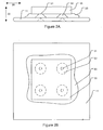
- Figure 6A is a side view of an embodiment of the invention wherein the lead-frame has four circular shaped dimples and the integrated circuit die is attached to the raised portions of the dimples.
- Figure 6B is a top view of the lead-frame mounting structure and attached die shown in Figure 6A.
- Figure 7A is a side view of an embodiment of the invention having an X-shaped dimple wherein the integrated circuit die is attached to the raised portion of the dimple.
- Figure 7B is a top view of the lead-frame and attached die shown in Figure 7A.
- Figure 8A is a side view of an embodiment of the invention wherein the lead-frame has a circular dimple and the integrated circuit die is attached to a raised portion of the dimple.
- Figure 8B is a top view of the lead-frame and attached die shown in Figure 8A.
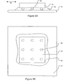
- Figure 9A is a side view of an embodiment of the invention having inserts or spacers between the lead-frame mounting structure and the attached die wherein the inserts or spacers are between the lead-frame and the die.
- Figure 9B is a top view of the lead-frame and attached die shown in Figure 9A.
- the mounting structure is a lead frame 11 and the spreaders are dimples 30.
- An integrated circuit die 10 is attached to the lead-frame 11 by die attach adhesive 20.
- the lead-frame 11 has four dimples 30. Each dimple 30 is a circular dimple having a top 31.
- the integrated circuit die 10 rests on the top 31 of each dimple 30.
- the die attach adhesive 20 is disposed between the integrated circuit die 10 and the lead-frame 11 and is interposed about the dimples 30.
- the integrated circuit die 10 is square and the dimples 30 are located in the lead-frame 11 so as to be positioned under the four corners of the integrated circuit die 10.
- the lead frame 11 supports the integrated circuit die 10 indirectly through the adhesive 20, the integrated circuit die 10 is supported directly by the spreaders, which in this case are dimples 30.
- the spreaders which in this case are dimples 30.
- a thin layer of adhesive 20 is also found between the tops 31 of the dimples 30 and the integrated circuit die 10, but this layer is typically so thin it is negligible when considering the effect of the lead frame on the die during thermal expansion.
- the surface area of the dimples 30 are relatively small, even when added together, compared to the surface area of the remaining portion of the lead frame directly under the integrated circuit die 10. Thus, only a small portion of the mounting structure (dimples 30) are in direct contact with the integrated circuit die 10.
- the integrated circuit die 10 and lead frame 11 expand and contract at different rates. Since a majority of the material comprising the lead-frame 11 is aligned in the horizontal direction 39, most of the dimensional changes of the lead-frame 11 are in the horizontal direction 39.
- the material comprising the dimples 30 expands partially in the vertical direction 38. Expansion in the vertical direction 38 only increases the separation distance of the lead frame 11 and the die 10 and does not induce stress in the die 10. Further, since the die is separated from the lead frame 11, the expansion of the lead frame in the horizontal direction 39 is absorbed by the die attach material 20. Therefore, this configuration significantly reduces the amount of stress induced in the die 10 due to thermal expansion.
- the mounting structure is a lead frame 11 and the spreaders are ridges 35.
- the lead-frame 11 is angled or bent to form ridges 35.
- the ridges 35 extend across the entire length of the integrated circuit die 10.
- two ridges 35 are formed parallel to each other.
- Each ridge 35 has a top 31 to which the integrated circuit die 10 is attached.
- the integrated circuit die 10 is attached to the lead-frame 11 by die attach adhesive 20.
- Each ridge 35 has a pair of vertical portions 36 which are joined by horizontal portion 37.
- the horizontal portion forms the top 31 upon which the integrated circuit die 10 is attached.
- the lead-frame 11 expands and contracts with changes in temperature according to its coefficient of thermal expansion. Since a majority of the material comprising the lead-frame 11 is aligned in the horizontal direction 39, most of the dimensional changes of the lead-frame 11 are in the horizontal direction 39. Further, since the integrated circuit die 10 is attached only to the tops 31 of the ridges 35, the integrated circuit die 10 is not significantly impacted by the thermal expansion of the lead-frame 11. Finally, thermal expansion of the vertical portions 36 of the ridges 35 only increases the distance between the integrated circuit die 10 and the lead-frame 11. Therefore, thermal expansion of the vertical portions 36 in the vertical direction 38 has no deleterious effect on the integrated circuit die 10.
- the mounting structure is a lead frame 11 and spreaders are dimples 30.
- Two dimples 30 are formed in the lead-frame 11 and are symmetrically positioned under the integrated circuit die 10.
- the dimples 30 are linear in form and are positioned parallel to each other.
- the integrated circuit die 10 is attached to the tops 31 of the dimples 30.
- the die attach adhesive 20 is between and around the dimples 30 so as to attach the integrated circuit die 10 to the lead-frame 11.
- the mounting structure is a lead frame 11 and spreader is a dimple 30.
- a single dimple 30 is formed in the lead-frame 11.
- the dimple 30 has the shape of an "X.” The distal portions of the "X" are positioned beneath each of the four comers of the integrated circuit die 10, respectively.
- the dimple 30 has a top 31 upon which the integrated circuit die 10 is attached.
- the die attach adhesive 20 is between the lead-frame 11 and the integrated circuit die 10 and surrounds the dimple 30.
- the mounting structure is a lead frame 11 and spreaders are dimples 30.
- dimples 30 are formed in the lead-frame 11.
- the dimples 30 are positioned beneath the sides at the midpoint between the corners of the integrated circuit die 10.
- the integrated circuit die 10 is attached to the tops 31 of the dimples 30 by the die attach adhesive 20 which is between the integrated circuit die 10 and the lead-frame 11.
- the mounting structure is a lead frame 11 and the spreader is a dimple 30.
- a single dimple 30 is formed in the lead-frame 11.
- the dimple 30 has the shape of a "T.”
- the distal ends of the dimple 30 are positioned beneath the sides, at the midpoint between the corners, of the integrated circuit die 10.
- the integrated circuit die 10 is attached to the top 31 of the dimple 30 by the die attach adhesive 20.
- the mounting structure is a lead frame 11 and the spreader is a dimple 30.
- a single dimple 30 is formed in the lead-frame 11.
- the dimple 30 is formed in the shape of a ring and is centrally located beneath the integrated circuit die 10.
- the integrated circuit die 10 is attached to a top 31 of the dimple 30 by the die attach adhesive 20.
- the die attach adhesive 20 is both on the inside and the outside of the circular dimple 30.
- the mounting structure is a lead frame 11 and the spreaders are spacers 40.
- the spacers 40 are positioned between the integrated circuit die 10 and the lead-frame 11.
- nine spacers 40 are positioned equidistant from each other symmetrically between the integrated circuit die 10 and the lead-frame 11.
- the integrated circuit die 10 is attached to the lead-frame 11 by die attach adhesive 20 with the spacers 40 between. Spacers 40 ensure that the integrated circuit die 10 is held at a constant distance from the lead-frame 11.
- the spacers 40 are balls. In alternative embodiments, the spacers are blocks, cylinders, wires, washers, disks, or any other geometric form known to persons of skill in the art.
- the purpose of the spacers is to support the integrated circuit die 10 on the lead-frame 11 through minimal contact so that the integrated circuit die is attached by a relatively thick portion of die attach adhesive 20 across a significant portion of the area between the integrated circuit die 10 and the lead-frame 11.
- the spacers 40 support the die 10 and ensure that the separation distance between the die 10 and the lead frame 11 is uniform across the entire area.
Landscapes
- Die Bonding (AREA)
- Lead Frames For Integrated Circuits (AREA)
Abstract
Description
Claims (20)
- A method for attaching an integrated circuit die to a mounting structure, the method comprising:forming a mounting structure having a die pad and at least one spreader;applying an adhesive to the die pad and the at least one spreader of said mounting structure; andattaching the integrated circuit die to the adhesive, wherein the at least one spreader is between the die pad and the integrated circuit die.
- A method as claimed in claim 1, wherein said at least one spreader is a dimple, and wherein said forming a mounting structure comprises pressing a dimple in the die pad from a side opposite a side of the die pad to which the integrated circuit die is to be attached.
- A method as claimed in claim 1, wherein said at least one spreader is a rib, and wherein said forming a mounting structure comprises bending a rib in the die pad.
- A method as claimed in claim 1, wherein said at least one spreader is a spacer, and wherein said forming a mounting structure comprises placing the spacer between the die pad and the integrated circuit die.
- A method as claimed in claim 4, wherein said spacer is a spacer selected from the group consisting of a ball, wire, block, cylinder, washer, and disk.
- A method as claimed in claim 1, further comprising encapsulating the integrated circuit die, the adhesive and the mounting structure in plastic.
- A method as claimed in claim 1, wherein an area of the integrated circuit die in contact with the at least one spreader is less than an area not in contact with the at least one spreader.
- An integrated circuit package comprising:a mounting structure having a die pad and at least one spreader;an adhesive adhered to the die pad and the at least one spreader of said mounting structure; andan integrated circuit die adhered to the adhesive, wherein the at least one spreader is between the die pad and the integrated circuit die.
- A package as claimed in claim 8, wherein said at least one spreader is a dimple, and wherein said dimple protrudes from a side of the die pad to which the integrated circuit die is adhered.
- A package as claimed in claim 8, wherein said at least one spreader is a rib, and wherein said rib is bent in the die pad and protrudes from a side of the die pad to which the integrated circuit die is adhered.
- A package as claimed in claim 8, wherein said at least one spreader is a spacer placed between the die pad and the integrated circuit die.
- A package as claimed in claim 11, wherein said spacer is a spacer selected from the group consisting of a ball, wire, block, cylinder, washer, and disk.
- A package as claimed in claim 8, further comprising plastic which encapsulates the integrated circuit die, the adhesive and the mounting structure.
- A package as claimed in claim 8, wherein an area of the integrated circuit die in contact with the at least one spreader is less than an area not in contact with the at least one spreader.
- A mounting structure for an integrated circuit die, said mounting structure comprising:a die pad for supporting the integrated circuit die; andat least one spreader for supporting the integrated circuit die at a distance from said die pad.
- A mounting structure as claimed in claim 15, wherein said at least one spreader is a dimple, and wherein said dimple protrudes from a side of the die pad to which the integrated circuit die is to be adhered.
- A mounting structure as claimed in claim 15, wherein said at least one spreader is a rib, and wherein said rib is bent in the die pad and protrudes from a side of the die pad to which the integrated circuit die is to be adhered.
- A mounting structure as claimed in claim 15, wherein said at least one spreader is a spacer placed adjacent the die pad on a side of the die pad to which the integrated circuit die is to be adhered.
- A mounting structure as claimed in claim 18, wherein said spacer is a spacer selected from the group consisting of a ball, wire, block, cylinder, washer, and disk.
- A mounting structure as claimed in claim 15, wherein an area of the die pad for supporting the integrated circuit die is greater than an area of the at least one spreader for supporting the integrated circuit die at a distance from said die pad.
Applications Claiming Priority (2)
| Application Number | Priority Date | Filing Date | Title |
|---|---|---|---|
| US527298 | 1990-05-23 | ||
| US09/527,298 US6306684B1 (en) | 2000-03-16 | 2000-03-16 | Stress reducing lead-frame for plastic encapsulation |
Publications (2)
| Publication Number | Publication Date |
|---|---|
| EP1134806A2 true EP1134806A2 (en) | 2001-09-19 |
| EP1134806A3 EP1134806A3 (en) | 2003-11-12 |
Family
ID=24100899
Family Applications (1)
| Application Number | Title | Priority Date | Filing Date |
|---|---|---|---|
| EP01103220A Withdrawn EP1134806A3 (en) | 2000-03-16 | 2001-02-12 | Stress reducing lead-frame for plastic encapsulation |
Country Status (6)
| Country | Link |
|---|---|
| US (1) | US6306684B1 (en) |
| EP (1) | EP1134806A3 (en) |
| JP (1) | JP2001284516A (en) |
| KR (1) | KR20010090489A (en) |
| CN (1) | CN1314709A (en) |
| TW (1) | TW503548B (en) |
Cited By (2)
| Publication number | Priority date | Publication date | Assignee | Title |
|---|---|---|---|---|
| DE10319782A1 (en) * | 2003-04-30 | 2004-11-25 | Osram Opto Semiconductors Gmbh | Chip carrier element especially for luminescent and laser diode chips, has recessed receiving area adjacent to the chip mounting surface to connect the chip |
| KR20170109669A (en) * | 2015-02-06 | 2017-09-29 | 엠케이에스 인스트루먼츠, 인코포레이티드 | Stress Relief MEMS Structures and Packages |
Families Citing this family (29)
| Publication number | Priority date | Publication date | Assignee | Title |
|---|---|---|---|---|
| US6357098B1 (en) * | 1998-12-04 | 2002-03-19 | Terastor Corporation | Methods and devices for positioning and bonding elements to substrates |
| US6683368B1 (en) * | 2000-06-09 | 2004-01-27 | National Semiconductor Corporation | Lead frame design for chip scale package |
| US6689640B1 (en) | 2000-10-26 | 2004-02-10 | National Semiconductor Corporation | Chip scale pin array |
| US6551859B1 (en) | 2001-02-22 | 2003-04-22 | National Semiconductor Corporation | Chip scale and land grid array semiconductor packages |
| DE10221085B4 (en) * | 2002-05-11 | 2012-07-26 | Robert Bosch Gmbh | Assembly having a connection device for contacting a semiconductor device and manufacturing method |
| JP2004179253A (en) * | 2002-11-25 | 2004-06-24 | Nec Semiconductors Kyushu Ltd | Semiconductor device and method of manufacturing the same |
| US7095096B1 (en) | 2004-08-16 | 2006-08-22 | National Semiconductor Corporation | Microarray lead frame |
| DE102004054062B3 (en) * | 2004-11-05 | 2006-03-02 | Danfoss Silicon Power Gmbh | Soldering system for heavy-duty semiconductor circuit uses spray of solder droplets in stream of hot gas to build up deposit of solder on area to be soldered |
| US7846775B1 (en) | 2005-05-23 | 2010-12-07 | National Semiconductor Corporation | Universal lead frame for micro-array packages |
| TW200723495A (en) * | 2005-12-07 | 2007-06-16 | Chipmos Technologies Inc | Chip package structure |
| US20070176271A1 (en) * | 2006-02-01 | 2007-08-02 | Stats Chippac Ltd. | Integrated circuit package system having die-attach pad with elevated bondline thickness |
| US8421093B2 (en) | 2007-07-13 | 2013-04-16 | Rohm Co., Ltd. | LED module and LED dot matrix display |
| US7808089B2 (en) * | 2007-12-18 | 2010-10-05 | National Semiconductor Corporation | Leadframe having die attach pad with delamination and crack-arresting features |
| US20090152683A1 (en) * | 2007-12-18 | 2009-06-18 | National Semiconductor Corporation | Rounded die configuration for stress minimization and enhanced thermo-mechanical reliability |
| US8802553B2 (en) | 2011-02-10 | 2014-08-12 | Infineon Technologies Ag | Method for mounting a semiconductor chip on a carrier |
| US8947886B2 (en) * | 2011-07-19 | 2015-02-03 | Infineon Technologies Ag | Electronic component |
| JP2014203861A (en) * | 2013-04-02 | 2014-10-27 | 三菱電機株式会社 | Semiconductor device and semiconductor module |
| MY184608A (en) | 2013-12-10 | 2021-04-07 | Carsem M Sdn Bhd | Pre-molded integrated circuit packages |
| JP2017037866A (en) * | 2013-12-26 | 2017-02-16 | パナソニック株式会社 | Semiconductor device |
| DE102014200126A1 (en) * | 2014-01-08 | 2014-12-04 | Robert Bosch Gmbh | Component with a semiconductor device on a support |
| CN104091765A (en) * | 2014-07-14 | 2014-10-08 | 深迪半导体(上海)有限公司 | Packaging method targeted for MEMS inertial device semiconductor |
| US9559077B2 (en) * | 2014-10-22 | 2017-01-31 | Nxp Usa, Inc. | Die attachment for packaged semiconductor device |
| EP3331007A1 (en) * | 2016-12-05 | 2018-06-06 | Melexis Technologies SA | Integrated circuit package comprising lead frame |
| WO2020175619A1 (en) * | 2019-02-28 | 2020-09-03 | 京セラ株式会社 | Electronic component mounting package, electronic device, and light-emitting device |
| CN110745772B (en) * | 2019-10-21 | 2023-10-20 | 重庆大学 | A MEMS stress isolation packaging structure and its manufacturing method |
| EP3958302A1 (en) * | 2020-08-17 | 2022-02-23 | Infineon Technologies AG | Base plate for a semiconductor module and method for producing a base plate |
| CN112318790B (en) * | 2020-09-09 | 2022-08-19 | 西安近代化学研究所 | Vulcanization molding process for high-viscosity silicon-based heat insulation layer |
| US12487254B2 (en) | 2021-08-23 | 2025-12-02 | Allegro Microsystems, Llc | Packaged current sensor integrated circuit |
| US12493057B2 (en) | 2023-11-17 | 2025-12-09 | Allegro Microsystems, Llc | Current sensor integrated circuit |
Family Cites Families (15)
| Publication number | Priority date | Publication date | Assignee | Title |
|---|---|---|---|---|
| US4388132A (en) * | 1981-06-01 | 1983-06-14 | Burroughs Corporation | Method of attaching a protective film to an integrated circuit |
| JPS58207645A (en) * | 1982-05-28 | 1983-12-03 | Fujitsu Ltd | Semiconductor device |
| US4942452A (en) * | 1987-02-25 | 1990-07-17 | Hitachi, Ltd. | Lead frame and semiconductor device |
| JPS63258026A (en) * | 1987-04-15 | 1988-10-25 | Mitsubishi Electric Corp | Die bonding method |
| JPH01243531A (en) * | 1988-03-25 | 1989-09-28 | Hitachi Ltd | Semiconductor device |
| JPH02146757A (en) * | 1988-11-28 | 1990-06-05 | Mitsubishi Electric Corp | Semiconductor device |
| JPH03149864A (en) * | 1989-11-07 | 1991-06-26 | Matsushita Electron Corp | Lead frame |
| DE69227937T2 (en) | 1991-02-12 | 1999-05-12 | Matsushita Electronics Corp., Kadoma, Osaka | Lead frames and resin sealed semiconductor device therefor |
| JPH04280439A (en) * | 1991-03-08 | 1992-10-06 | Fujitsu Ltd | Semiconductor device and manufacture thereof |
| JPH0547988A (en) * | 1991-08-21 | 1993-02-26 | Sony Corp | Semiconductor device |
| KR100386061B1 (en) * | 1995-10-24 | 2003-08-21 | 오끼 덴끼 고오교 가부시끼가이샤 | Semiconductor device and lead frame with improved construction to prevent cracking |
| SG46955A1 (en) * | 1995-10-28 | 1998-03-20 | Inst Of Microelectronics | Ic packaging lead frame for reducing chip stress and deformation |
| US5872398A (en) | 1996-01-11 | 1999-02-16 | Micron Technology, Inc. | Reduced stress LOC assembly including cantilevered leads |
| JP3558459B2 (en) * | 1996-02-08 | 2004-08-25 | 沖電気工業株式会社 | Inner lead connection method |
| US5818103A (en) | 1997-03-28 | 1998-10-06 | Nec Corporation | Semiconductor device mounted on a grooved head frame |
-
2000
- 2000-03-16 US US09/527,298 patent/US6306684B1/en not_active Expired - Lifetime
-
2001
- 2001-02-12 EP EP01103220A patent/EP1134806A3/en not_active Withdrawn
- 2001-03-14 JP JP2001073168A patent/JP2001284516A/en not_active Withdrawn
- 2001-03-14 CN CN01111468A patent/CN1314709A/en active Pending
- 2001-03-16 TW TW090106192A patent/TW503548B/en not_active IP Right Cessation
- 2001-03-16 KR KR1020010013776A patent/KR20010090489A/en not_active Withdrawn
Cited By (4)
| Publication number | Priority date | Publication date | Assignee | Title |
|---|---|---|---|---|
| DE10319782A1 (en) * | 2003-04-30 | 2004-11-25 | Osram Opto Semiconductors Gmbh | Chip carrier element especially for luminescent and laser diode chips, has recessed receiving area adjacent to the chip mounting surface to connect the chip |
| DE10319782B4 (en) * | 2003-04-30 | 2009-01-02 | Osram Opto Semiconductors Gmbh | Optoelectronic semiconductor component with a chip carrier element |
| KR20170109669A (en) * | 2015-02-06 | 2017-09-29 | 엠케이에스 인스트루먼츠, 인코포레이티드 | Stress Relief MEMS Structures and Packages |
| EP3253708A4 (en) * | 2015-02-06 | 2018-08-01 | MKS Instruments, Inc. | Stress relief mems structure and package |
Also Published As
| Publication number | Publication date |
|---|---|
| TW503548B (en) | 2002-09-21 |
| EP1134806A3 (en) | 2003-11-12 |
| CN1314709A (en) | 2001-09-26 |
| KR20010090489A (en) | 2001-10-18 |
| US6306684B1 (en) | 2001-10-23 |
| JP2001284516A (en) | 2001-10-12 |
Similar Documents
| Publication | Publication Date | Title |
|---|---|---|
| US6306684B1 (en) | Stress reducing lead-frame for plastic encapsulation | |
| US6348726B1 (en) | Multi row leadless leadframe package | |
| US7102209B1 (en) | Substrate for use in semiconductor manufacturing and method of making same | |
| US6458626B1 (en) | Fabricating method for semiconductor package | |
| US5053852A (en) | Molded hybrid IC package and lead frame therefore | |
| TWI515855B (en) | Lead frame package with improved ground bond stability | |
| KR101017533B1 (en) | Small mold locks for heat sinks or flags for overmolded plastic packages | |
| KR100586699B1 (en) | Semiconductor chip package and its manufacturing method | |
| US5633206A (en) | Process for manufacturing lead frame for semiconductor package | |
| US8741694B1 (en) | Placing heat sink into packaging by strip formation assembly | |
| WO2007146775A2 (en) | Stacked chips with underpinning | |
| WO2008083146A1 (en) | Stress-resistant leadframe and method | |
| CN212750875U (en) | A semiconductor heat sink device | |
| KR100268756B1 (en) | A structure of seperat type diepad for leadframe | |
| JPH0344040A (en) | Semiconductor device and its manufacture | |
| JPH02202042A (en) | Resin-sealed semiconductor device | |
| TWI240396B (en) | Thermal enhanced chip package with wire bonding | |
| JPH1117082A (en) | Resin-sealed semiconductor device | |
| KR100265460B1 (en) | Lead frame having die pad of type buffer | |
| KR100483460B1 (en) | FBGA package using elastomer which shaping enlarged molding area | |
| KR940008336B1 (en) | Semiconductor package | |
| KR940000746B1 (en) | Chip bonding method of semiconductor | |
| JPH08125051A (en) | Semiconductor device | |
| JPS61240664A (en) | Semiconductor device | |
| KR200141125Y1 (en) | Structure of lead frame |
Legal Events
| Date | Code | Title | Description |
|---|---|---|---|
| PUAI | Public reference made under article 153(3) epc to a published international application that has entered the european phase |
Free format text: ORIGINAL CODE: 0009012 |
|
| 17P | Request for examination filed |
Effective date: 20010212 |
|
| AK | Designated contracting states |
Kind code of ref document: A2 Designated state(s): AT BE CH CY DE DK ES FI FR GB GR IE IT LI LU MC NL PT SE TR |
|
| AX | Request for extension of the european patent |
Free format text: AL;LT;LV;MK;RO;SI |
|
| PUAL | Search report despatched |
Free format text: ORIGINAL CODE: 0009013 |
|
| AK | Designated contracting states |
Kind code of ref document: A3 Designated state(s): AT BE CH CY DE DK ES FI FR GB GR IE IT LI LU MC NL PT SE TR |
|
| AX | Request for extension of the european patent |
Extension state: AL LT LV MK RO SI |
|
| AKX | Designation fees paid |
Designated state(s): AT BE CH CY DE DK ES FI FR GB GR IE IT LI LU MC NL PT SE TR |
|
| STAA | Information on the status of an ep patent application or granted ep patent |
Free format text: STATUS: THE APPLICATION IS DEEMED TO BE WITHDRAWN |
|
| 18D | Application deemed to be withdrawn |
Effective date: 20040513 |