EP1134557B1 - Verfahren zum Unterbringen von Sensoren in einen Gehäuse - Google Patents
Verfahren zum Unterbringen von Sensoren in einen Gehäuse Download PDFInfo
- Publication number
- EP1134557B1 EP1134557B1 EP01890065A EP01890065A EP1134557B1 EP 1134557 B1 EP1134557 B1 EP 1134557B1 EP 01890065 A EP01890065 A EP 01890065A EP 01890065 A EP01890065 A EP 01890065A EP 1134557 B1 EP1134557 B1 EP 1134557B1
- Authority
- EP
- European Patent Office
- Prior art keywords
- housing
- sensors
- hollow space
- cavity
- sensor
- Prior art date
- Legal status (The legal status is an assumption and is not a legal conclusion. Google has not performed a legal analysis and makes no representation as to the accuracy of the status listed.)
- Expired - Lifetime
Links
Images
Classifications
-
- H10W74/01—
-
- G—PHYSICS
- G01—MEASURING; TESTING
- G01F—MEASURING VOLUME, VOLUME FLOW, MASS FLOW OR LIQUID LEVEL; METERING BY VOLUME
- G01F1/00—Measuring the volume flow or mass flow of fluid or fluent solid material wherein the fluid passes through a meter in a continuous flow
- G01F1/68—Measuring the volume flow or mass flow of fluid or fluent solid material wherein the fluid passes through a meter in a continuous flow by using thermal effects
- G01F1/684—Structural arrangements; Mounting of elements, e.g. in relation to fluid flow
- G01F1/6845—Micromachined devices
-
- G—PHYSICS
- G01—MEASURING; TESTING
- G01F—MEASURING VOLUME, VOLUME FLOW, MASS FLOW OR LIQUID LEVEL; METERING BY VOLUME
- G01F15/00—Details of, or accessories for, apparatus of groups G01F1/00 - G01F13/00 insofar as such details or appliances are not adapted to particular types of such apparatus
- G01F15/14—Casings, e.g. of special material
-
- H10W72/536—
-
- H10W72/5363—
-
- H10W74/10—
-
- H10W90/756—
Definitions
- the invention relates to a method for accommodating sensors in a housing, in particular of chemical,
- the invention now aims to provide a method of the type mentioned, in which the assembly costs can be substantially reduced and at the same time the necessary connections can be formed in a cost effective manner with a few process steps.
- the inventive method consists essentially in that in a first step, the active sensor surface of a semiconductor or IC sensor is provided with a cavity on the active sensor surface forming cap and the sensor is connected to contacts or bonding wires in that subsequently the housing is formed by casting, in particular injection molding, and that in a third method step or simultaneously with the second method step the cavity formed above the active sensor surface is opened.
- the casting of chips with a suitable potting compound for many electronic components is known.
- the known methods are generally not suitable for sensors which must be in contact with the outside world after casting the sensor is no longer accessible without costly reworking and in the event of subsequent processing, the risk of damage to the sensor can not be excluded.
- the active sensor surface of a semiconductor or IC sensor is provided with a cap forming a cavity over the active sensor surface in a first method step, the corresponding active sensor surface is kept free by the potting compound to be subsequently applied.
- the attachment of bonding wires as is customary in chip production, can be accomplished in a simple manner with conventional devices, wherein in a subsequent casting process, in particular an injection molding, a finished component is created directly, which already has all the electrical contacts.
- the active sensor surface in turn can be suitably brought into contact with the environment, for which either simultaneously with the second process step, with which the housing is molded or molded, or in connection to this second process step the cavity is mechanically opened.
- the opening of the cavity in a third downstream process step is hiebei compared to the simultaneous formation of the opening not least because a simultaneous opening of the cavity requires that when closing the mold or the injection mold directly through the wall of the cavity forming cap is pierced. Since at this time the injection molding compound is not hardened in most cases, this would mean that the previously positioned sensor is moved within the casting compound, unless a corresponding abutment is provided on the opposite side.
- the cavity is opened after at least partial hardening of the potting compound by sawing and / or drilling.
- the housing may be formed of suitable plastics, for which a number of plastics in semiconductor technology has been proven accordingly.
- an optical sensor can advantageously be opened by drilling the cavity, whereupon a light guide is inserted into the open cavity.
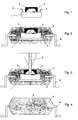
- FIG. 1 a section through a sensor
- Fig. 2 a section through the built-in a housing sensor
- Fig. 3 a cut accordingly Fig. 2 with a schematically illustrated machining tool for opening the cavity
- Fig. 4 a view of the sensor after opening the cavity
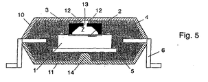
- Fig. 5 an alternative method step for forming the opening of the cavity in a representation corresponding to Fig. 2 ,
- Fig. 1 1 denotes a sensor IC whose sensor surface 2 is arranged on the outside of the IC.
- a cap 3 forming a cavity above the active sensor surface 2 is then placed and the electrical contacting is effected via bonding wires 4.
- FIG. 2 the housing is visible after the injection process and schematically denoted by 5.
- a leadframe 6, which has the corresponding bonding wires, is already integrated into the housing 5 and the remaining cavity 7 above the active sensor surface 2 can be seen.
- FIG. 3 In the presentation after Fig. 3 is now a saw indicated by 8, which separates the outer wall of the housing 5 and the cap 3 accordingly, so that an open connection to the cavity 7 is provided, in which the active sensor element 2 is located.
- Fig. 4 shows the sensor produced in this way in a view whose opening 9 allows the access of the outside world to the active sensor element 2 inside the housing 5.
- Fig. 5 Now, the process step for the production of the housing with simultaneous formation of an opening in a representation corresponding to Fig. 2 again clarified.
- process step of a subsequent opening of the cavity can be omitted.
- the cavity forming the cap 3 is already equipped with an opening, wherein the injection mold must now have appropriate modifications.
- the mold consists hiebei of a first mold half 10 and a second mold half 11, wherein the first mold half 10, which is adjacent to the cap 3, inwardly projecting webs 12, which are sealingly pressed against the cap outside the already provided opening 13 of the cap.
- the second mold half 11 has a corresponding pressure piece 14, whereby the webs 12 can be pressed correspondingly close to the cap 3, so that immediately after demolding an open access to the cavity 7 is formed.
- encapsulated and correspondingly built in a housing sensors can be produced in a cost effective manner with a few suitable for mass production and mass production steps.
Landscapes
- Physics & Mathematics (AREA)
- Fluid Mechanics (AREA)
- General Physics & Mathematics (AREA)
- Encapsulation Of And Coatings For Semiconductor Or Solid State Devices (AREA)
- Injection Moulding Of Plastics Or The Like (AREA)
- Measuring Fluid Pressure (AREA)
- Light Receiving Elements (AREA)
Description
- Die Erfindung bezieht sich auf ein Verfahren zum Unterbringen von Sensoren in einem Gehäuse, insbesondere von chemischen,
- Durchfluß-, oder optischen Sensoren in einem Kunststoffgehäuse, wie z.B. beschrieben in
DE-A-42 19 575 ,US-A-4 697 203 oderJP-A-09 304 211 - Chemische Sensoren, ebenso wie Durchfluß- oder optische Sensoren können bereits in integrierter Form mit üblichen Chipherstellungsverfahren kostengünstig und mit hoher Präzision hergestellt werden. Derartige IC-Sensoren bzw. Chipsensoren mußten aber in der Folge unter hohem Montageaufwand in einem Gehäuse eingebaut werden, wobei das Gehäuse in aller Regel entweder verschraubt oder verklebt wurde und die Anschlüsse an die Sensoren in entsprechender Weise aus dem Gehäuse herausgeführt werden mußten. Dies gilt nicht nur für die elektrischen Anschlüsse, sondern bei chemischen-, Durchflußrate- oder optischen Sensoren naturgemäß auch für Leitungsanschlüsse oder Lichtleiteranschlüsse, für die eine entsprechende zusätzliche Bearbeitung der Gehäuse erforderlich war. Für die Herstellung derartiger Sensoren war somit die Unterbringung in einem Gehäuse ein kostenbestimmender Faktor für die Massenproduktion.
- Die Erfindung zielt nun darauf ab, ein Verfahren der eingangs genannten Art zu schaffen, bei welchem der Montageaufwand wesentlich verringert werden kann und gleichzeitig die erforderlichen Anschlüsse in kostengünstiger Weise mit wenigen Verfahrensschritten ausgebildet werden können. Zur Lösung dieser Aufgabe besteht das erfindungsgemäße Verfahren im wesentlichen darin, daß in einem ersten Verfahrensschritt die aktive Sensorfläche eines Halbleiter- bzw. IC-Sensors mit einer einen Hohlraum über der aktiven Sensorfläche ausbildenden Kappe versehen wird und der Sensor mit Kontakten bzw. Bonddrähten verbunden wird, daß anschließend das Gehäuse durch Gießen, insbesondere Spritzgießen, angeformt und daß in einem dritten Verfahrensschritt oder gleichzeitig mit dem zweiten Verfahrensschritt der über der aktiven Sensorfläche ausgebildete Hohlraum geöffnet wird. Prinzipiell ist das Vergießen von Chips mit einer geeigneten Vergußmasse für viele elektronische Bauteile bekannt. Die bekannten Verfahren eignen sich jedoch durchwegs nicht für Sensoren, welche in Kontakt mit der Außenwelt stehen müssen, da nach dem Vergießen der Sensor nicht mehr ohne aufwendige Nachbearbeitung zugänglich wird und im Falle einer nachträglichen Bearbeitung die Gefahr einer Beschädigung des Sensors nicht ausgeschlossen werden kann. Dadurch, daß nun erfindungsgemäß in einem ersten Verfahrensschritt die aktive Sensorfläche eines Halbleiter- bzw. IC-Sensors mit einer einen Hohlraum über der aktiven Sensorfläche ausbildenden Kappe versehen wird, wird die entsprechende aktive Sensorfläche von der nachher aufzubringenden Vergußmasse freigehalten. Die Anbringung von Bonddrähten, wie dies bei der Chipherstellung üblich ist, läßt sich mit konventionellen Einrichtungen in einfacher Weise bewerkstelligen, wobei bei einem nachfolgenden Gießvorgang, insbesondere einem Spritzgießvorgang, unmittelbar ein fertiger Bauteil geschaffen wird, welcher bereits alle elektrischen Kontakte aufweist. Es muß somit lediglich sichergestellt werden, daß die aktive Sensorfläche in geeigneter Weise wiederum mit der Umwelt in Kontakt gebracht werden kann, wofür entweder gleichzeitig mit dem zweiten Verfahrensschritt, mit welchem das Gehäuse angegossen bzw. angeformt wird, oder aber in Anschluß an diesen zweiten Verfahrensschritt der Hohlraum mechanisch geöffnet wird. Die Öffnung des Hohlraumes in einem dritten nachgeschalteten Verfahrensschritt ist hiebei gegenüber der gleichzeitigen Ausbildung der Öffnung nicht zuletzt deshalb bevorzugt weil eine gleichzeitige Öffnung des Hohlraumes erfordert, daß beim Schließen der Gußform bzw. der Spritzgußform unmittelbar die Wand der den Hohlraum ausbildenden Kappe durchstoßen wird. Da zu diesem Zeitpunkt die Spritzgußmasse in aller Regel nicht erhärtet ist, hätte dies zur Folge, daß der zuvor positionierte Sensor innerhalb der Gußmasse verschoben wird, wenn nicht ein entsprechendes Widerlager auf der Gegenseite vorgesehen ist. Wenn Spritzguß mit entsprechend höherem Druck vorgenommen wird, müßte in diesem Falle auch sichergestellt werden, daß die Gußform die Kappe dichtend durchtrennt, um zu verhindern, daß Grußmasse in den Hohlraum eingepreßt werden kann. Mit Vorteil wird daher im Rahmen des erfindungsgemäßen Verfahrens so vorgegangen, daß der Hohlraum nach dem zumindest teilweisen Erhärten der Vergußmasse durch Sägen und/oder Bohren geöffnet wird.
- In besonders einfacher Weise kann das Gehäuse aus geeigneten Kunststoffen ausgebildet sein, wofür eine Reihe von Kunststoffen in der Halbleitertechnologie sich entsprechend bewährt hat.
- Im Falle der Verwendung eines optischen Sensors kann mit Vorteil der Hohlraum durch Bohren geöffnet werden, worauf in den geöffneten Hohlraum ein Lichtleiter eingeführt wird.
- Für eine gleichzeitige Ausbildung der elektrischen Kontakte für das Einsetzen eines derartigen mit einem Gehäuse versehenen Sensors in einen Sockel oder in eine entsprechend vorbereitete Leiterplatte kann mit Vorteil so vorgegangen werden, daß die Bonddrähte mit einem Rahmen mit Kontaktstiften verbunden sind und daß der Rahmen unter Freilassen der Kontaktstifte in die Vergußmasse eingebettet wird.
- Die Erfindung wird nachfolgend anhand der in der Zeichnung schematisch dargestellten einzelnen Verfahrensschritte näher erläutert. In dieser zeigen
Fig. 1 einen Schnitt durch einen Sensor,Fig. 2 einen Schnitt durch den in ein Gehäuse eingebauten Sensor,Fig. 3 einen Schnitt entsprechendFig. 2 mit einem schematisch dargestellten Bearbeitungswerkzeug zum Öffnen des Hohlraumes,Fig. 4 eine Ansicht des Sensors nach dem Öffnen des Hohlraumes undFig. 5 einen alternativen Verfahrensschritt zur Ausbildung der Öffnung des Hohlraumes in einer Darstellung entsprechend derFig. 2 . - In
Fig. 1 ist 1 ein Sensor-IC bezeichnet, dessen Sensorfläche 2 an der Außenseite des ICs angeordnet ist. Im ersten Verfahrensschritt wird nun eine einen Hohlraum über der aktiven Sensorfläche 2 ausbildende Kappe 3 aufgesetzt und die elektrische Kontaktierung über Bonddrähte 4 vorgenommen. - In
Fig. 2 ist das Gehäuse nach dem Spritzvorgang ersichtlich und schematisch mit 5 bezeichnet. Ein Leadframe 6, welcher die entsprechenden Bonddrähte aufweist, ist bereits in das Gehäuse 5 integriert und es ist der verbleibende Hohlraum 7 oberhalb der aktiven Sensorfläche 2 ersichtlich. - Bei der Darstellung nach
Fig. 3 ist nun eine Säge mit 8 angedeutet, welche die Außenwand des Gehäuses 5 und die Abdeckkappe 3 entsprechend auftrennt, sodaß eine offene Verbindung zum Hohlraum 7 geschaffen wird, in welchem sich das aktive Sensorelement 2 befindet. -
Fig. 4 zeigt den auf diese Weise hergestellten Sensor in einer Ansicht, dessen Öffnung 9 den Zugang der Außenwelt zum aktiven Sensorelement 2 im Inneren des Gehäuses 5 ermöglicht. - In
Fig. 5 wird nun der Verfahrensschritt zur Herstellung des Gehäuses unter gleichzeitiger Ausbildung einer Öffnung in einer Darstellung entsprechend derFig. 2 nochmals verdeutlicht. Bei dieser Verfahrensweise kann auf den inFig. 3 dargestellten Verfahrensschritt einer nachträglichen Öffnung des Hohlraumes verzichtet werden. Bei dieser Ausbildung ist nun die den Hohlraum ausbildende Kappe 3 bereits mit einer Durchbrechung ausgestattet, wobei die Spritzgußform nunmehr entsprechende Modifikationen aufweisen muß. Die Form besteht hiebei aus einer ersten Formhälfte 10 und einer zweiten Formhälfte 11, wobei die erste Formhälfte 10, welche der Kappe 3 benachbart ist, einwärts ragende Stege 12 aufweist, welche dichtend an die Kappe außerhalb der bereits vorgesehenen Durchbrechung 13 der Kappe angepreßt werden. Zu diesem Zweck weist die zweite Formhälfte 11 ein entsprechendes Druckstück 14 auf, womit die Stege 12 entsprechend dicht an die Kappe 3 angepreßt werden können, sodaß nach dem Entformen unmittelbar ein offener Zugang zum Hohlraum 7 ausgebildet wird. - Insgesamt lassen sich somit mit wenigen für die Serien- und Massenfertigung geeigneten Verfahrensschritten verkapselte und entsprechend in einem Gehäuse eingebaute Sensoren in kostengünstiger Weise herstellen.
Claims (5)
- Verfahren zum Unterbringen von Sensoren in einem Gehäuse (5), insbesondere von chemischen, Durchfluß-, oder optischen Sensoren in einem Kunststoffgehäuse, dadurch gekennzeichnet, daß in einem ersten Verfahrensschritt die aktive Sensorfläche (2) eines Halbleiter- bzw. IC-Sensors (1) mit einer einen Hohlraum (7) über der aktiven Sensorfläche (2) ausbildenden Kappe (3) versehen wird und der Sensor (1) mit Kontakten bzw. Bonddrähten (4) verbunden wird, daß in einem zweiten Verfahrensschritt das Gehäuse (5) durch Gießen, insbesondere Spritzgießen, angeformt und daß in einem dritten Verfahrensschritt oder gleichzeitig mit dem zweiten Verfahrensschritt der über der aktiven Sensorfläche (2) ausgebildete Hohlraum (7) geöffnet wird.
- Verfahren nach Anspruch 1, dadurch gekennzeichnet, daß der Hohlraum (7) nach dem zumindest teilweisen Erhärten der Vergußmasse durch Sägen und/oder Bohren geöffnet wird.
- Verfahren nach Anspruch 1 oder 2, dadurch gekennzeichnet, daß das Gehäuse (5) aus Kunststoffen ausgebildet wird.
- Verfahren nach Anspruch 1, 2 oder 3, dadurch gekennzeichnet, daß in den geöffneten Hohlraum (7) ein Lichtleiter eingeführt wird.
- Verfahren nach einem der Ansprüche 1 bis 4, dadurch gekennzeichnet, daß die Bonddrähte (4) mit einem Rahmen (6) mit Kontaktstiften verbunden sind und daß der Rahmen (6) unter Freilassen der Kontaktstifte in die Vergußmasse eingebettet wird.
Applications Claiming Priority (2)
| Application Number | Priority Date | Filing Date | Title |
|---|---|---|---|
| AT0042000A AT410727B (de) | 2000-03-14 | 2000-03-14 | Verfahren zum unterbringen von sensoren in einem gehäuse |
| AT4202000 | 2000-03-14 |
Publications (3)
| Publication Number | Publication Date |
|---|---|
| EP1134557A2 EP1134557A2 (de) | 2001-09-19 |
| EP1134557A3 EP1134557A3 (de) | 2003-01-08 |
| EP1134557B1 true EP1134557B1 (de) | 2008-10-15 |
Family
ID=3673925
Family Applications (1)
| Application Number | Title | Priority Date | Filing Date |
|---|---|---|---|
| EP01890065A Expired - Lifetime EP1134557B1 (de) | 2000-03-14 | 2001-03-07 | Verfahren zum Unterbringen von Sensoren in einen Gehäuse |
Country Status (4)
| Country | Link |
|---|---|
| US (1) | US6395585B2 (de) |
| EP (1) | EP1134557B1 (de) |
| AT (1) | AT410727B (de) |
| DE (1) | DE50114411D1 (de) |
Families Citing this family (41)
| Publication number | Priority date | Publication date | Assignee | Title |
|---|---|---|---|---|
| DE10054013B4 (de) | 2000-11-01 | 2007-06-21 | Robert Bosch Gmbh | Drucksensormodul |
| US20020079572A1 (en) | 2000-12-22 | 2002-06-27 | Khan Reza-Ur Rahman | Enhanced die-up ball grid array and method for making the same |
| US6420201B1 (en) * | 2001-01-03 | 2002-07-16 | Amkor Technology, Inc. | Method for forming a bond wire pressure sensor die package |
| JP4037117B2 (ja) * | 2001-02-06 | 2008-01-23 | 株式会社日立製作所 | 表示装置 |
| US6891239B2 (en) * | 2002-03-06 | 2005-05-10 | The Charles Stark Draper Laboratory, Inc. | Integrated sensor and electronics package |
| US7304362B2 (en) * | 2002-05-20 | 2007-12-04 | Stmicroelectronics, Inc. | Molded integrated circuit package with exposed active area |
| WO2004048955A2 (en) * | 2002-11-27 | 2004-06-10 | City Technology Limited | Gas sensing device |
| GB0227686D0 (en) | 2002-11-27 | 2003-01-08 | City Tech | Gas sensing device |
| US7335971B2 (en) * | 2003-03-31 | 2008-02-26 | Robert Bosch Gmbh | Method for protecting encapsulated sensor structures using stack packaging |
| GB0307616D0 (en) * | 2003-04-02 | 2003-05-07 | Melexis Nv | Calorimetric flow meter |
| DE102004027512A1 (de) * | 2004-06-04 | 2005-12-22 | Robert Bosch Gmbh | Spektroskopischer Gassensor, insbesondere zum Nachweis mindestens einer Gaskomponente in der Umluft, und Verfahren zur Herstellung eines derartigen spektroskopischen Gassensors |
| DE102004031317A1 (de) | 2004-06-29 | 2006-01-19 | Robert Bosch Gmbh | Gassensormodul und Verfahren zu seiner Herstellung |
| GB0504379D0 (en) * | 2005-03-03 | 2005-04-06 | Melexis Nv | Low profile overmoulded semiconductor package with transparent lid |
| EP1860694A1 (de) * | 2005-03-16 | 2007-11-28 | Yamaha Corporation | Halbleiterbauelement, verfahren zur herstellung eines halbleiterbauelements und abdeckrahmen |
| US7859071B2 (en) * | 2005-03-31 | 2010-12-28 | Finisar Corporation | Power and communication interface for sensors using a single tethered fiber |
| US8154414B2 (en) * | 2005-03-31 | 2012-04-10 | Finisar Corporation | Systems and methods for collecting data with sensors |
| WO2006114005A1 (en) * | 2005-04-27 | 2006-11-02 | Sensirion Ag | A method for packaging integrated sensors |
| EP1717562A1 (de) * | 2005-04-29 | 2006-11-02 | Sensirion AG | Verfahren zum Verkapseln von integrierten Sensoren |
| US8302471B2 (en) * | 2005-12-02 | 2012-11-06 | Melexis Nv | Calorimetric flow meter having high heat conductivity strips |
| US7808004B2 (en) * | 2006-03-17 | 2010-10-05 | Edison Opto Corporation | Light emitting diode package structure and method of manufacturing the same |
| MX2008014073A (es) | 2006-05-04 | 2008-11-28 | Touchsensor Tech Llc | Sensor de fluidos en linea. |
| EP1860417B1 (de) * | 2006-05-23 | 2011-05-25 | Sensirion Holding AG | Drucksensor mit einer Kammer und Herstellungsverfahren dafür |
| EP1860418A1 (de) * | 2006-05-23 | 2007-11-28 | Sensirion AG | Verfahren zur Herstellung eines Drucksensors unter Verwendung von SOI-Wafern |
| US7402459B2 (en) * | 2006-07-10 | 2008-07-22 | Shanghai Kaihong Technology Co., Ltd. | Quad flat no-lead (QFN) chip package assembly apparatus and method |
| EP1700724B1 (de) * | 2006-07-19 | 2009-09-02 | Sensirion Holding AG | Feuchtigkeitsfühler zur Ermittlung von Beschlag auf einem Fenster |
| ITMI20072099A1 (it) * | 2007-10-30 | 2009-04-30 | St Microelectronics Srl | Metodo di fabbricazione di un dispositivo elettronico comprendente dispositivi mems incapsulati per stampaggio |
| CN101533783B (zh) * | 2008-03-13 | 2011-05-04 | 上海凯虹电子有限公司 | 薄型四侧扁平无引脚封装方法 |
| EP2154713B1 (de) * | 2008-08-11 | 2013-01-02 | Sensirion AG | Verfahren zur Herstellung einer Messvorrichtung mit einer Spannungsverminderungsschicht |
| EP2159558A1 (de) * | 2008-08-28 | 2010-03-03 | Sensirion AG | Verfahren zur Herstellung eines integrierten Drucksensors |
| US8360390B2 (en) * | 2009-01-13 | 2013-01-29 | Enphase Energy, Inc. | Method and apparatus for potting an electronic device |
| EP2224218B1 (de) * | 2009-02-25 | 2018-11-28 | Sensirion Automotive Solutions AG | Sensor in einer geformten Verpackung und Herstellungsverfahren dafür |
| EP2573804A1 (de) * | 2011-09-21 | 2013-03-27 | Nxp B.V. | Integrierte Schaltung mit Sensor und Verfahren zur Ihrer Herstellung |
| JP6041053B2 (ja) * | 2013-06-10 | 2016-12-07 | 富士電機株式会社 | 半導体装置及びその製造方法 |
| EP2871456B1 (de) | 2013-11-06 | 2018-10-10 | Invensense, Inc. | Drucksensor und Herstellungsmethode für einen Drucksensor |
| EP2871455B1 (de) | 2013-11-06 | 2020-03-04 | Invensense, Inc. | Drucksensor |
| EP2765410B1 (de) * | 2014-06-06 | 2023-02-22 | Sensirion AG | Sensorbaustein |
| EP3032227B1 (de) | 2014-12-08 | 2020-10-21 | Sensirion AG | Flusssensorpaket |
| EP3614115B1 (de) | 2015-04-02 | 2024-09-11 | InvenSense, Inc. | Drucksensor |
| US11225409B2 (en) | 2018-09-17 | 2022-01-18 | Invensense, Inc. | Sensor with integrated heater |
| WO2020236661A1 (en) | 2019-05-17 | 2020-11-26 | Invensense, Inc. | A pressure sensor with improve hermeticity |
| CN115472577A (zh) * | 2021-06-11 | 2022-12-13 | 恩智浦美国有限公司 | 集成电路封装和制造集成电路封装的方法 |
Family Cites Families (12)
| Publication number | Priority date | Publication date | Assignee | Title |
|---|---|---|---|---|
| JPS60257546A (ja) * | 1984-06-04 | 1985-12-19 | Mitsubishi Electric Corp | 半導体装置及びその製造方法 |
| JPS6350745A (ja) * | 1986-08-20 | 1988-03-03 | Fuji Photo Film Co Ltd | 化学センサ− |
| JPH05203522A (ja) * | 1992-01-23 | 1993-08-10 | Mitsubishi Electric Corp | モールドパッケージ半導体圧力センサおよびその製造方法 |
| KR960009089B1 (ko) * | 1993-03-04 | 1996-07-10 | 문정환 | 패키지 성형용 금형 및 그 금형을 이용한 플라스틱 고체촬상소자 패키지 제조방법 및 패키지 |
| KR970005706B1 (ko) * | 1994-01-24 | 1997-04-19 | 금성일렉트론 주식회사 | 고체촬상소자 및 그 제조방법 |
| JP3366460B2 (ja) * | 1994-09-19 | 2003-01-14 | 新光電気工業株式会社 | 片面樹脂封止型半導体パッケージ並びに片面樹脂封止型半導体装置及びその製造方法 |
| US5808872A (en) * | 1994-11-15 | 1998-09-15 | Nippon Steel Corporation | Semiconductor package and method of mounting the same on circuit board |
| JPH09304211A (ja) * | 1996-05-15 | 1997-11-28 | Omron Corp | 静電容量型圧力センサのパッケージング構造およびパッケージング方法 |
| NL1003315C2 (nl) * | 1996-06-11 | 1997-12-17 | Europ Semiconductor Assembly E | Werkwijze voor het inkapselen van een geïntegreerde halfgeleiderschake- ling. |
| GB2316225A (en) * | 1996-08-06 | 1998-02-18 | Northern Telecom Ltd | Semiconductor photodetector packaging |
| US5918112A (en) * | 1997-07-24 | 1999-06-29 | Motorola, Inc. | Semiconductor component and method of fabrication |
| DE19929025A1 (de) * | 1999-06-25 | 2000-12-28 | Bosch Gmbh Robert | Drucksensor |
-
2000
- 2000-03-14 AT AT0042000A patent/AT410727B/de not_active IP Right Cessation
-
2001
- 2001-03-07 EP EP01890065A patent/EP1134557B1/de not_active Expired - Lifetime
- 2001-03-07 DE DE50114411T patent/DE50114411D1/de not_active Expired - Lifetime
- 2001-03-13 US US09/804,148 patent/US6395585B2/en not_active Expired - Fee Related
Also Published As
| Publication number | Publication date |
|---|---|
| US20010023087A1 (en) | 2001-09-20 |
| ATA4202000A (de) | 2002-11-15 |
| EP1134557A3 (de) | 2003-01-08 |
| US6395585B2 (en) | 2002-05-28 |
| AT410727B (de) | 2003-07-25 |
| DE50114411D1 (de) | 2008-11-27 |
| EP1134557A2 (de) | 2001-09-19 |
Similar Documents
| Publication | Publication Date | Title |
|---|---|---|
| EP1134557B1 (de) | Verfahren zum Unterbringen von Sensoren in einen Gehäuse | |
| DE68929367T2 (de) | Kartenmodul für integrierte Schaltung | |
| DE69737248T2 (de) | Verfahren zum Einkapseln einer integrierten Halbleiterschaltung | |
| DE69519938T2 (de) | Kapsel für ein optoelektrisches bauelement mit einer optischen schnittstelle | |
| DE10008203B4 (de) | Verfahren zum Herstellen elektronischer Halbleiterbauelemente | |
| EP1622237A1 (de) | Optisches oder elektronisches Modul und Verfahren zu dessen Herstellung | |
| DE102007005630B4 (de) | Sensorchip-Modul und Verfahren zur Herstellung eines Sensorchip-Moduls | |
| WO2015079027A1 (de) | Optoelektronisches bauelement und verfahren zu seiner herstellung | |
| DE102010001711A1 (de) | Halbleiter-Bauelement und entsprechendes Herstellungsverfahren | |
| EP1646854A1 (de) | Sensoreinrichtung | |
| EP0649719B1 (de) | Verfahren zur Herstellung von Chipkarten mittels Spritzgiessen | |
| DE10250540B3 (de) | Verfahren zur Herstellung eines optoelektronischen Bauteiles | |
| EP1630913B1 (de) | Verfahren zum Herstellen eines mit einem Kunststoffgehäuse versehenen optischen oder elektronischen Moduls das eine optische oder elektronische Komponente enthält, sowie optisches oder elektronisches Modul | |
| EP2265102A1 (de) | Sensoraufbau ohne Gehäuse | |
| DE69116517T2 (de) | Halbleitender photoelektrischer Detektor mit einer vertikalen optischen Achse | |
| EP0664524B1 (de) | Verfahren zum Verkappen eines Chipkartenmoduls | |
| DE10153615C1 (de) | Verfahren zur Herstellung von elektronischen Bauteilen | |
| DE102018104382A1 (de) | Optoelektronisches bauelement und herstellungsverfahren | |
| DE102019006445B4 (de) | Verfahren zur Herstellung eines Bauteils | |
| EP0817116A2 (de) | Chipkarte sowie Verfahren und Herstellung einer Chipkarte | |
| DE2623715A1 (de) | Modulare schaltungsanordnung | |
| DE10154543A1 (de) | Kunststoffspritzgußteil mit optischer Anzeigefunktion und Verfahren zur Herstellung des Spritzgußteils | |
| EP1236227B1 (de) | Verfahren und herstellung eines sensors | |
| EP1411467A1 (de) | Tragbarer Datenträger mit Display | |
| EP0691626A2 (de) | Datenträger mit einem Modul mit integriertem Schaltkreis |
Legal Events
| Date | Code | Title | Description |
|---|---|---|---|
| PUAI | Public reference made under article 153(3) epc to a published international application that has entered the european phase |
Free format text: ORIGINAL CODE: 0009012 |
|
| AK | Designated contracting states |
Kind code of ref document: A2 Designated state(s): AT BE CH CY DE DK ES FI FR GB GR IE IT LI LU MC NL PT SE TR |
|
| AX | Request for extension of the european patent |
Free format text: AL;LT;LV;MK;RO;SI |
|
| PUAL | Search report despatched |
Free format text: ORIGINAL CODE: 0009013 |
|
| AK | Designated contracting states |
Kind code of ref document: A3 Designated state(s): AT BE CH CY DE DK ES FI FR GB GR IE IT LI LU MC NL PT SE TR |
|
| AX | Request for extension of the european patent |
Free format text: AL;LT;LV;MK;RO;SI |
|
| RIC1 | Information provided on ipc code assigned before grant |
Free format text: 7G 01D 11/24 A, 7H 01L 21/56 B, 7G 01F 1/684 B |
|
| 17P | Request for examination filed |
Effective date: 20021220 |
|
| AKX | Designation fees paid |
Designated state(s): DE FR GB IT |
|
| GRAP | Despatch of communication of intention to grant a patent |
Free format text: ORIGINAL CODE: EPIDOSNIGR1 |
|
| GRAS | Grant fee paid |
Free format text: ORIGINAL CODE: EPIDOSNIGR3 |
|
| GRAA | (expected) grant |
Free format text: ORIGINAL CODE: 0009210 |
|
| AK | Designated contracting states |
Kind code of ref document: B1 Designated state(s): DE FR GB IT |
|
| REG | Reference to a national code |
Ref country code: GB Ref legal event code: FG4D Free format text: NOT ENGLISH |
|
| REF | Corresponds to: |
Ref document number: 50114411 Country of ref document: DE Date of ref document: 20081127 Kind code of ref document: P |
|
| PLBE | No opposition filed within time limit |
Free format text: ORIGINAL CODE: 0009261 |
|
| STAA | Information on the status of an ep patent application or granted ep patent |
Free format text: STATUS: NO OPPOSITION FILED WITHIN TIME LIMIT |
|
| 26N | No opposition filed |
Effective date: 20090716 |
|
| REG | Reference to a national code |
Ref country code: FR Ref legal event code: PLFP Year of fee payment: 16 |
|
| PGFP | Annual fee paid to national office [announced via postgrant information from national office to epo] |
Ref country code: IT Payment date: 20160323 Year of fee payment: 16 |
|
| REG | Reference to a national code |
Ref country code: FR Ref legal event code: PLFP Year of fee payment: 17 |
|
| PG25 | Lapsed in a contracting state [announced via postgrant information from national office to epo] |
Ref country code: IT Free format text: LAPSE BECAUSE OF NON-PAYMENT OF DUE FEES Effective date: 20170307 |
|
| REG | Reference to a national code |
Ref country code: FR Ref legal event code: PLFP Year of fee payment: 18 |
|
| PGFP | Annual fee paid to national office [announced via postgrant information from national office to epo] |
Ref country code: GB Payment date: 20180327 Year of fee payment: 18 |
|
| PGFP | Annual fee paid to national office [announced via postgrant information from national office to epo] |
Ref country code: FR Payment date: 20180326 Year of fee payment: 18 |
|
| PGFP | Annual fee paid to national office [announced via postgrant information from national office to epo] |
Ref country code: DE Payment date: 20180328 Year of fee payment: 18 |
|
| REG | Reference to a national code |
Ref country code: DE Ref legal event code: R119 Ref document number: 50114411 Country of ref document: DE |
|
| GBPC | Gb: european patent ceased through non-payment of renewal fee |
Effective date: 20190307 |
|
| PG25 | Lapsed in a contracting state [announced via postgrant information from national office to epo] |
Ref country code: GB Free format text: LAPSE BECAUSE OF NON-PAYMENT OF DUE FEES Effective date: 20190307 Ref country code: DE Free format text: LAPSE BECAUSE OF NON-PAYMENT OF DUE FEES Effective date: 20191001 |
|
| PG25 | Lapsed in a contracting state [announced via postgrant information from national office to epo] |
Ref country code: FR Free format text: LAPSE BECAUSE OF NON-PAYMENT OF DUE FEES Effective date: 20190331 |