EP1133051A1 - Circuit mélangeur - Google Patents
Circuit mélangeur Download PDFInfo
- Publication number
- EP1133051A1 EP1133051A1 EP01410024A EP01410024A EP1133051A1 EP 1133051 A1 EP1133051 A1 EP 1133051A1 EP 01410024 A EP01410024 A EP 01410024A EP 01410024 A EP01410024 A EP 01410024A EP 1133051 A1 EP1133051 A1 EP 1133051A1
- Authority
- EP
- European Patent Office
- Prior art keywords
- differential
- coupled
- signal
- transistor
- transistors
- Prior art date
- Legal status (The legal status is an assumption and is not a legal conclusion. Google has not performed a legal analysis and makes no representation as to the accuracy of the status listed.)
- Granted
Links
Images


Classifications
-
- H—ELECTRICITY
- H03—ELECTRONIC CIRCUITRY
- H03D—DEMODULATION OR TRANSFERENCE OF MODULATION FROM ONE CARRIER TO ANOTHER
- H03D7/00—Transference of modulation from one carrier to another, e.g. frequency-changing
- H03D7/14—Balanced arrangements
- H03D7/1425—Balanced arrangements with transistors
- H03D7/1441—Balanced arrangements with transistors using field-effect transistors
-
- H—ELECTRICITY
- H03—ELECTRONIC CIRCUITRY
- H03D—DEMODULATION OR TRANSFERENCE OF MODULATION FROM ONE CARRIER TO ANOTHER
- H03D7/00—Transference of modulation from one carrier to another, e.g. frequency-changing
- H03D7/14—Balanced arrangements
- H03D7/1425—Balanced arrangements with transistors
- H03D7/1458—Double balanced arrangements, i.e. where both input signals are differential
-
- H—ELECTRICITY
- H03—ELECTRONIC CIRCUITRY
- H03D—DEMODULATION OR TRANSFERENCE OF MODULATION FROM ONE CARRIER TO ANOTHER
- H03D7/00—Transference of modulation from one carrier to another, e.g. frequency-changing
- H03D7/14—Balanced arrangements
- H03D7/1425—Balanced arrangements with transistors
- H03D7/1483—Balanced arrangements with transistors comprising components for selecting a particular frequency component of the output
-
- H—ELECTRICITY
- H03—ELECTRONIC CIRCUITRY
- H03D—DEMODULATION OR TRANSFERENCE OF MODULATION FROM ONE CARRIER TO ANOTHER
- H03D7/00—Transference of modulation from one carrier to another, e.g. frequency-changing
- H03D7/16—Multiple-frequency-changing
- H03D7/165—Multiple-frequency-changing at least two frequency changers being located in different paths, e.g. in two paths with carriers in quadrature
-
- H—ELECTRICITY
- H03—ELECTRONIC CIRCUITRY
- H03D—DEMODULATION OR TRANSFERENCE OF MODULATION FROM ONE CARRIER TO ANOTHER
- H03D2200/00—Indexing scheme relating to details of demodulation or transference of modulation from one carrier to another covered by H03D
- H03D2200/0001—Circuit elements of demodulators
- H03D2200/0023—Balun circuits
-
- H—ELECTRICITY
- H03—ELECTRONIC CIRCUITRY
- H03D—DEMODULATION OR TRANSFERENCE OF MODULATION FROM ONE CARRIER TO ANOTHER
- H03D2200/00—Indexing scheme relating to details of demodulation or transference of modulation from one carrier to another covered by H03D
- H03D2200/0001—Circuit elements of demodulators
- H03D2200/0033—Current mirrors
-
- H—ELECTRICITY
- H03—ELECTRONIC CIRCUITRY
- H03D—DEMODULATION OR TRANSFERENCE OF MODULATION FROM ONE CARRIER TO ANOTHER
- H03D2200/00—Indexing scheme relating to details of demodulation or transference of modulation from one carrier to another covered by H03D
- H03D2200/0041—Functional aspects of demodulators
- H03D2200/0043—Bias and operating point
Definitions
- the present invention relates to improvement of a mixer circuit used in a receiver in digital radio communication system, in particular, relates to such a circuit which is excellent in image rejection.
- Fig. 6 shows in general an image rejection mixer circuit, in which a received RF (radio frequency) signal is applied to a pair of multipliers 61 and 62, each of which receives further, a local signal LO, directly or through a 90° phase shifter 63, so that a product of RF and LO is obtained. Then, each multiplier provides a pair of output frequencies F RF +F LO and F RF -F LO , where the former is undesired frequency and the latter is desired IF frequency. A product of each multipliers is applied to a low pass filter 64, 65, so that a pair of IF signals having the phase difference of 90° are obtained. Then, two IF signals are added in an adder 67 after one of the IF signals is shifted by 90° in a phase shifter 66, so that image rejection is carried out.
- a received RF radio frequency
- a pair of multipliers and a 90° phase shifter are used as shown in Fig. 6.
- a prior mixer of Fig. 6 has the disadvantage that an image rejection in GHz band is not enough as a 90° phase shifter with excellent performance in GHz band is difficult.
- Fig. 7 is a conventional Gilbert-cell mixer, in which a radio frequency signal RF is applied to a pair of input transistors 71 and 72 located in lower position in the figure. Therefore, an output signal amplitude of a Gilbert-cell type circuit depends upon a gain of input transistors 71 and 72.
- an image rejection ratio (IRR) would be degraded if two IF signals (inphase component, and quadrature component) have amplitude error between two components or phase error from 90° between two components, and the IRR is expressed as follows (described in RF Microelectronics, Rehzad Razavi, Prentice Hall PTR, page 143). IRR ⁇ ⁇ ( ⁇ A IF /A IF ) 2 +( ⁇ IF ) 2 ⁇ /4
- One of the reasons which causes an IF signal error is an error or a dispersion of mixer circuits. For instance, if two mixer circuits have an error of 2% in amplitude with each other, IRR would be degraded by approximate 40 dB.
- Fig. 8 is a prior quadrature mixer circuit which reduces affection by an amplitude error of a mixer circuit (International Conference ISSCC93-TP9.4).
- the circuit of Fig. 8 has two Gilbert-cell mixers of Fig. 7, and the sources of the RF signal input transistors 81, 82, 83 and 84 are coupled together with each other.
- the Fig. 8 circuit receives a pair of local signals LO-I and LO-Q having quadrature relation, and an RF signal in balance form or differential form, and provides a pair of IF signals IF-I and IF-Q having quadrature relation, where -I means inphase component, and -Q means quadrature component.
- the circuit of Fig. 8 has the disadvantage that amplitude error exists between IF-I and IF-Q, since RF signal input transistors have an error in gain between 81 and 82, and between 83 and 84.
- a differential pair for mixing inphase component LO-I of a local signal with an RF signal is supplied an RF signal through the transistor 81
- a differential pair for mixing quadrature component LO-Q of a local signal with an RF signal is supplied an RF signal through the transistor 82
- the difference of the gain of the transistors 81 and 82 causes an error of amplitude of an output IF signal between inphase component and quadrature component.
- Fig. 9 is the improvement of Fig. 8 for removing amplitude error between IF-I and IF-Q, by feeding an RF input signal to both differential pairs for inphase component and quadrature component by using a common differential pair (91 and 92).
- phase error of output IF signals is larger than phase error of local signals (LO-I, LO-Q), when a pair of local signals (LO-I, LO-Q) have phase error ( ⁇ LO : radian) from 90°.
- a Fig. 9 circuit is constituted by using a CMOS having gate length 0.2 ⁇ m, the following result is obtained in the circuit simulation using HSPICE. ⁇ IF ⁇ 1.4 ⁇ LO
- a bias potential of a differential pair 2 for mixing a local signal with an RF signal can not be independent from a bias potential of a transistor of a differential amplifier for an input RF signal.
- a bias potential of a differential pair affects much to phase of an output IF signal.
- transistors 91 and 92 of a differential amplifier are biased through a resistor connected to a gate of each transistor, and a bias transistor 93, which is used in the Gilbert-cell mixer of Fig. 7.
- the transistors of differential pairs 2 are biased through a resistor connected to a gate of each transistor, and a bias current in the differential amplifier 91, 92.
- bias current in the differential amplifier 91, 92 affects to bias current in the differential pairs 2. Therefore, it is impossible to bias the differential pairs 2 to the optimum bias potential to obtain the minimum phase error of an output IF signal.
- the present mixer circuit receives an RF input signal, and a first local signal LO-I in differential form, and a second local signal LO-Q in differential form.
- the first local signal LO-I is an inphase component of the local signal
- the second local signal LO-Q is a quadrature component of the local signal.
- the quadrature component has the phase relation with the inphase component that the phase of the former is shifted by 90° from that of the quadrature component.
- the present mixer circuit provides an output IF signal having an inphase component IF-I and a quadrature component IF-Q in differential form.
- the frequency of the output IF signal is generally the difference between the frequency of the input RF signal and the frequency of the local signal.
- a plurality of differential pairs each having a pair of transistors are provided for mixing each signal (a, b) of each component (LO-I, LO-Q) of a local signal (LO) with each signal (a, b) of an RF signal (RF).
- An input RF signal is amplified by using a differential amplifier which has a pair of transistors.
- Each differential pair receives a local signal (LO-I, LO-Q) each having signals (a, b) at a gate of each transistors, and an output of said differential amplifier at a source of the transistors.
- An output of a transistor of each differential pair is combined with an output of a transistor of another differential pair, and provides a component of an output IF signal.
- First essential feature of the present invention is that a source of each differential pairs and a differential amplifier is coupled with a power source potential through an impedance circuit which has high impedance for operational frequency of the circuit and short-circuited for D.C. current.
- This allows to provide a bias potential to a gate of a transistor of a differential pair independently from a bias potential of a gate of a transistor of a differential amplifier.
- An independent bias potential allows a differential pair and a differential amplifier to have optimized bias potential so that a phase error of an output IF signal is the minimum, in other words, a quadrature component of an output IF signal has the exact phase relation of 90° with an inphase component of an output IF signal.
- a differential pair of inphase component and a differential pair of quadrature component are supplied an RF input signal directly by each transistor of a differential amplifier. This allows to decrease a phase error of an output IF signal than a phase error of a local signal. Assuming that a local signal LO has some phase error, then, a transistor of a differential pair driven by an inphase component of a local signal would simultaneously open or close with a transistor of a differential pair driven by a quadrature component of a local signal. Then, a RF current signal supplied by a differential amplifier is shared between the differential pairs. Thus, the amplitude of an IF output is decreased, then, causes a phase error of an output IF signal to be decreased.
- Said impedance circuit may be a tank circuit having a parallel circuit of a capacitor and an inductor, resonating with operational frequency, an input RF frequency, or a local frequency.
- said impedance circuit may be a mere inductor, having large impedance for operational frequency, and short-circuited for D.C. current.
- Fig. 1 is a quadrature mixer circuit of the first embodiment according to the present invention.
- the numeral 1 is a differential amplifier
- 2a, 2b, 2c, 2d and 2e are a differential transistor pair
- 3a, 3b and 3c are an impedance circuit
- 4 is a load of a transistor.
- an RF receive signal in balanced form or differential form is applied to a gate of an RF input differential pair 2e, whose sources are coupled with a second power source or grounded through a third impedance circuit 3c, and whose drains are coupled with a first power potential VDD through loads ZL1.
- a signal in balanced form is also called a signal in differential form.
- a signal in unbalanced form is called a single-ended signal.
- a first local signal LO-I is in balanced form having terminals (a) and (b), similarly, a second local signal LO-Q is in balanced form having quadrature relation with the first local signal LO-I, having terminals (a) and (b).
- a first terminal (a) of the first local signal LO-I is connected to a gate of a first transistor 2a-1 of a first differential pair 2a, and a gate of a second transistor 2b-2 of a second differential pair 2b.
- a second terminal (b) of a first local signal LO-I is connected to a gate of a second transistor 2a-2 of a first differential pair 2a and a gate of a first transistor 2b-1 of a second differential pair 2b.
- a first terminal (a) of a second local signal LO-Q is connected to a gate of a first transistor 2c-1 of a third differential pair 2c, and a gate of a second transistor 2d-2 of a fourth differential pair 2d.
- a second terminal (b) of a second local signal LO-Q is connected to a gate of a second transistor 2c-2 of a third differential pair 2c, and a gate of a first transistor 2d-1 of a fourth differential pair.
- the sources of the transistors 2a-1 and 2a-2 of the first differential pair 2a, and the sources of the transistors 2c-1 and 2c-2 of the third differential pair 2c are grounded through a first impedance circuit 3a, and are coupled with a drain of a first transistor 2e-1 of the differential amplifier 2e through a capacitor C.
- the sources of the transistors 2b-1 and 2b-2 of the second differential pair 2b, and the sources of the transistors 2d-1 and 2d-2 of the fourth differential pair 2d are grounded through a second impedance circuit 3b, and are coupled with a drain of a second transistor 2e-2 of the differential amplifier 2e through another capacitor C.
- a drain of the first transistor 2a-1 of the first differential pair 2a and a drain of the first transistor 2b-1 of the second differential pair 2b are coupled with the first potential VDD through a load ZL2, and coupled with a first terminal (a) of a first intermediate frequency output IF-I in balanced form.
- a drain of the second transistor 2a-2 of the first differential pair 2a and a drain of the second transistor 2b-2 of the second differential pair 2b are coupled with a first potential VDD through a load ZL2, and are coupled with a second terminal (b) of the first intermediate frequency output IF-I.
- a drain of the first transistor 2c-1 of the third differential pair 2c and a drain of the first transistor 2d-1 of the fourth differential pair 2d are coupled with the first potential VDD through a load ZL2, and coupled with a first terminal (a) of a second intermediate frequency output IF-Q in balanced form.
- a drain of the second transistor 2c-2 of the third differential pair 2c and a drain of the second transistor 2d-2 of the fourth differential pair 2d are coupled with a first potential VDD through a load ZL2, and are coupled with a second terminal (b) of the second intermediate frequency output IF-Q.
- the second output signal IF-Q is in quadrature relation with the first output signal IF-I.
- Each of the impedance circuits 3a, 3b and 3c has a capacitor CT and an inductor LT which resonate at operational frequency, input frequency RF, and local frequency LO.
- said impedance circuit may be an inductor which has large impedance at the operational frequency, and is essentially short-circuited for D.C. current.
- Fig. 1 it has a pair of complemental type mixer circuits for inphase signal (I), and quadrature signal (Q), respectively.
- the differential amplifier 2e which accepts an RF signal, and a pair of impedance circuits 3a and 3b, are common to a first mixer for inphase signal (I) and a second mixer for quadrature signal (Q). That structure allows phase error between IF-I and IF-Q to decrease than that between local signals LO-I and LO-Q.
- the impedance circuit As each of the impedance circuits has large impedance at the operational frequency, the impedance circuit is considered to be open in A.C. operation at the operational frequency, while it is short-circuited in D.C. operation. Therefore, the operation of Fig. 1 is equivalent in A.C. operation to that of Fig. 9.
- the phase error between IF-I and IF-Q is much decreased. Assuming that there exists a phase error on a local signal between LO-I and LO-Q, transistors in differential pairs for inphase component and quadrature component would open simultaneously.
- phase error of output IF signal is smaller than that of input local signal.
- the present invention has the advantage that an operational bias potential of the differential pairs 2a through 2d is independent from an operational bias potential of the differential amplifier 2e.
- the operational bias potential of the differential pairs 2a through 2d is supplied to a gate of a transistor through a resistor R coupled with the first source potential VDD, and the operational bias potential of the differential amplifier 2e is supplied to a gate of a transistor through another resistor r coupled with the first source potential VDD.
- phase error between output signals IF-I and IF-Q depends upon an operational bias potential
- Fig. 2 shows the relations between D.C. bias potential of a transistor which receives a local signal LO (horizontal axis) and the ratio of the phase error of an output IF signal to the phase error of a local signal LO.
- Fig. 2 is the simulation result by using the circuit simulator HSPICE, and has the assumption that the circuit of Fig. 1 is constituted by using a CMOS with gate length 0.2 ⁇ m. It should be noted in Fig. 2 that when a D.C.
- the phase error of the output IF signals is: ⁇ IF ⁇ 0.8 ⁇ LO ,
- Fig. 1 embodiment is improved by more than 5 dB in phase error as compared with the prior art of Fig. 9.
- a prior art of Fig. 8 and a prior art of Fig. 9 can not have the advantage of Fig. 1.
- the Fig. 8 circuit supplies an input RF signal to an I-branch mixer and a Q-branch mixer through different transistors so that amplitude of an input RF signal in I-branch mixer might be different from amplitude of an input RF signal in Q-branch mixer. This causes an amplitude error of output IF signals between IF-I and IF-Q.
- the Fig. 9 circuit has the disadvantage that a D.C. bias potential between a gate and a source of a transistor of the differential pairs 2a through 2d depends upon a D.C. bias potential of the differential amplifier 2e, and the former is in general higher than the latter by approximate 0.2 V.
- Fig. 3 shows the second embodiment of a quadrature mixer circuit according to the present invention.
- the features of Fig. 3 as compared with Fig. 1 are that an RF input differential amplifier is constituted by using a PMOS transistor, instead of an NMOS transistor, and that a drain of an RF input transistor is directly connected to sources of differential pairs which receive a local signal LO (no capacitor is used).
- an operational bias potential of an input RF differential amplifier can be independent from an operational bias potential of differential pairs which receive a local signal LO. Therefore, the Fig. 3 embodiment has the similar effect to that of the Fig. 1 embodiment.
- No load resistor ZL1 is used in Fig. 3 embodiment, instead, an impedance circuit 3c functions as a load. This allows to improve the phase error of an output IF signal (IF-I and IF-Q) than the Fig. 1 embodiment.
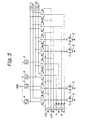
- Fig. 4 shows the third embodiment of the present invention.
- Fig. 4 is a complex mixer circuit having a real mixer and an imaginary mixer.
- a complex mixer circuit has the advantage that a phase error and an amplitude error of an output signal are small.
- the Fig. 4 embodiment comprises a pair of quadrature mixers of Fig. 1, and has a feature that a local signal LO and a load impedance are common to both a read mixer and an imaginary mixer.
- Bias resistors R and r exist in the Fig. 4 embodiment, but are not shown for the sake of simplicity of the figure.
- Each of the quadrature mixers in Fig. 4 carries out the multiplication of a pair of RF signals having quadrature relations with each other in balanced form, and a pair of local signals LO having quadrature relations with each other in balanced form.
- a load impedance is common, first products are added, and the other products are subtracted, to provide an output IF signal.
- a complex mixer circuit has the advantage that an error component in an output IF signal is decreased, since an error component of an output IF signal is only a product component of an error component of an input RF signal and an error component of a local signal LO, as described in "CMOS Wereless Transceiver Design, Jan Crols and Michiel Steyaert, Kluwer Academic Publishers, p179".
- the Fig. 4 embodiment has the similar effect to that of the Fig. 1 embodiment, so that a phase error in local signals LO is decreased. Thus, an error in an output IF signal is considerably decreased.
- an input RF signal is in balanced form, therefore, a differential amplifier for converting an input signal in unbalanced form to balanced form is omitted. It is a matter of course that an input RF signal may be in single-ended form (unbalanced form), which is converted to balanced form by using a differential amplifier 2e as shown in Fig. 1.
- Fig. 5 is a modification of Fig. 4.
- the feature of the Fig. 5 modification is that IF-I is the sum of the product of L02-I and RF-I and the product of LO2-Q and RF-Q, and IF-Q is the difference between the product of LO2-Q and RF-I and the product of L02-Q and RF-Q, while in the Fig. 4 embodiment IF-I is the difference between the product of LO2-I and RF-I and the product of LO2-Q and RF-Q, and IF-Q is the sum of the product of L02-Q and RF-I and the product of LO2-Q and RF-Q.
- a differential pair for accepting a local signal LO in Figs. 1, 4 and 5 are constituted by using an NMOS transistor.
- a differential pair may be constituted by using a PMOS transistor, in that case, a source potential and a ground potential are exchanged with each other.
- an impedance circuit or a tank circuit, is used as a constant current source.
- a constant current source may be an inductor or an RF choke coil having high impedance in operational frequency and being essentially short-circuited to D.C. current.
- an impedance circuit may be substituted with a conventional current source having a transistor with a fixed gate potential.
- the present mixer circuit can provide a radio receiver with a high degree image rejection by decreasing a phase error in an output IF signal than that in an input LO signal.
- conversion loss is as small as possible, and a pair of converted signals are well balanced with small amplitude error.
- Fig. 10 is a differential amplifier for converting an input signal Vin in unbalanced form into a pair of output signals Vout1 and Vout2 in balanced form.
- the transistors M3 and M4 constitute a current mirror circuit so that the transistor M3 functions as a constant current source.
- a tank circuit K having a parallel circuit of a capacitor CT and an inductor LT is coupled between a source of the transistor M3 and the ground, so that negative feed back is obtained with the impedance of the tank circuit K.
- An input signal Vin in single-ended form is applied to a gate of a transistor M1 which constitutes a differential amplifier with a transistor M2, and a gate of the other transistor M2 receives a fixed bias potential Vbias.
- a pair of outputs Vout1 and Vout2 in balanced form are obtained at outputs of the transistors M1 and M2.
- a tank circuit K has impedance ZT
- the output impedance Z0 is Z0 ⁇ v/i ⁇ 1/j ⁇ Cgd3.
- the current source may be replaced approximately by the capacitance Cgd3 between the gate and the drain of the transistor M3.
- a model for a small signal of the unbalance/balance converter in Fig. 10 is expressed as shown in Fig. 12. It is assumed that the gate width of the transistor Ml is equal to the gate width of the transistor M2, and the gate width of the transistor M3 is k times as large as that of the transistor M1. That small signal model introduces the following simultaneous equations, where a suffix shows a parameter of a transistor relating to a figure (1 or 2) of transistors M1 and M2, and Vgsl is voltage between a gate and a source of the transistor M1.
- a parameter (Cgd, Cgs, rds) relating to the same size is used with no suffix.
- Fig. 13 shows the result of the simulation using the circuit simulator HSPICE of the unbalance/balance converter of Fig. 10 at 2.45 GHz, where the horizontal axis is the size factor k of the transistor M3, and the vertical axis shows the ratio of the absolute value of the sum of two outputs (Vout1+Vout2) to the absolute value of one of the outputs (Vout1) in dB.
- the size factor k is the ratio of the gate width of a transistor for a current source to the gate width of a transistor for a differential pair, and the gate width of a current source transistor is k times as large as the gate width of a differential pair transistor. It should be noted in the figure that when 1.5 ⁇ k ⁇ 3 is satisfied, a desirable differential outputs are obtained.
- the optimum size factor k is approximate 2.2 since Vgs2 ⁇ -Vgs1.
- Fig. 14 shows another simulation result using the circuit simulator HSPICE of the unbalance/balance converter of Fig. 10.
- the figure shows the relations between frequency (horizontal axis) and differential output characteristics (vertical axis) when the value k is fixed to 2.0. It should be noted that between 2.4 GHz and 2.5 GHz, the value of the vertical axis is between -31 dB and -33 dB (curve (c)). This means that the differential output error is improved by 14-20 dB as compared with a prior unbalance/balance conversion circuit (curve(a) or curve (b)).
- Fig. 14 shows that the circuit is optimized for 2.4 - 2.5 GHz, the circuit may be optimized to any frequency by modifying the resonance frequency of the tank circuit K. Further, when a plurality of tank circuits each having different resonance frequency with each other are cascade connected, a differential amplifier for unbalance/balance converter may operate for a plurality of frequencies.
- the embodiment shows the case that a gate of a current source transistor M3 is biased by a current mirror circuit. Said gate may be biased by any bias means, such as a resistor ladder type source voltage divider.
- Fig. 15 shows the modification of a differential amplifier for unbalance/balance converter.
- the features of Fig. 15 are that a PMOS transistor is used, instead of an NMOS transistor, and a power source potential and a ground potential are reversed.
- the operation of Fig. 15 is the same as that of Fig. 10.
- a tank circuit K may be replaced by an inductor.
- Fig. 16 shows the combination of the quadrature mixer circuit of Fig. 1 and the converter from a single-ended input signal to a differential-output of Fig. 10.
- a differential amplifier 2e has a pair of transistors 2e-1 and 2e-2, which are indicated by M1 and M2.
- the sources of the transistors M1 and M2 are grounded through another transistor M3 and an impedance circuit or a tank circuit 3c.
- a signal-ended RF signal is applied to a gate of the transistor M1, while a gate of the other transistor M2 is biased by the fixed bias potential Bias2 which is further coupled with the gate of the transistor M1 through a resistor for biasing the transistor M1.
- the gate of the transistor M3 is biased by another bias potential Bias1.
- the drains of the transistors M1 and M2 are coupled with the power potential VDD through a load ZL1.
- Fig. 16 operates with a single-ended RF input by converting a single-ended signal to a differential signal at the input stage of a quadrature mixer circuit.
- Fig. 17 shows the combination of Fig. 3 and Fig. 15, where a PMOS transistor is used.
Landscapes
- Engineering & Computer Science (AREA)
- Power Engineering (AREA)
- Amplifiers (AREA)
- Superheterodyne Receivers (AREA)
Applications Claiming Priority (4)
| Application Number | Priority Date | Filing Date | Title |
|---|---|---|---|
| JP2000063485 | 2000-03-08 | ||
| JP2000063485A JP3522630B2 (ja) | 2000-03-08 | 2000-03-08 | 単相信号/差動信号変換型の電圧増幅器 |
| JP2000070318A JP2001257538A (ja) | 2000-03-14 | 2000-03-14 | 直交ミキサ回路及び複素ミキサ回路 |
| JP2000070318 | 2000-03-14 |
Publications (2)
| Publication Number | Publication Date |
|---|---|
| EP1133051A1 true EP1133051A1 (fr) | 2001-09-12 |
| EP1133051B1 EP1133051B1 (fr) | 2006-06-07 |
Family
ID=26587023
Family Applications (1)
| Application Number | Title | Priority Date | Filing Date |
|---|---|---|---|
| EP01410024A Expired - Lifetime EP1133051B1 (fr) | 2000-03-08 | 2001-03-07 | Circuit mélangeur |
Country Status (3)
| Country | Link |
|---|---|
| US (1) | US6871057B2 (fr) |
| EP (1) | EP1133051B1 (fr) |
| DE (1) | DE60120256T2 (fr) |
Cited By (5)
| Publication number | Priority date | Publication date | Assignee | Title |
|---|---|---|---|---|
| EP1418665A1 (fr) * | 2002-03-15 | 2004-05-12 | Mitsubishi Denki Kabushiki Kaisha | Convertisseur de frequence |
| WO2007074411A2 (fr) * | 2005-12-26 | 2007-07-05 | Dsp Group Switzerland Ag | Émetteur, terminal de télécommunication et procédé utilisant l’émetteur |
| WO2008001256A2 (fr) * | 2006-06-27 | 2008-01-03 | Nxp B.V. | Circuit mélangeur et son procédé de fonctionnement |
| CN102412786A (zh) * | 2011-12-20 | 2012-04-11 | 东南大学 | 一种跨导增强无源混频器 |
| CN101331679B (zh) * | 2005-12-15 | 2012-09-19 | Lm爱立信电话有限公司 | 接收器电路和无线通信设备 |
Families Citing this family (31)
| Publication number | Priority date | Publication date | Assignee | Title |
|---|---|---|---|---|
| US8816750B2 (en) | 2002-07-17 | 2014-08-26 | Broadcom Corporation | High frequency mixer with tunable dynamic range |
| JP4354681B2 (ja) * | 2002-09-13 | 2009-10-28 | 株式会社日立製作所 | 通信用半導体集積回路 |
| US7808937B2 (en) | 2005-04-07 | 2010-10-05 | Rambus, Inc. | Variable interference cancellation technology for CDMA systems |
| US20040127172A1 (en) * | 2002-12-27 | 2004-07-01 | Agere Systems Inc. | Phase-error suppressor and a method of suppressing phase-error |
| KR100539978B1 (ko) * | 2003-04-28 | 2006-01-10 | 삼성전자주식회사 | 주파수 혼합 회로 및 방법과 고주파 수신회로 및 방법 |
| US8351891B2 (en) * | 2003-05-30 | 2013-01-08 | The Regents Of The University Of California | Wideband distributed mixers |
| US6940352B2 (en) * | 2003-11-26 | 2005-09-06 | Scintera Networks, Inc. | Analog signal interpolation |
| US7254380B2 (en) * | 2004-07-22 | 2007-08-07 | Wen Kuei-Ann | Low flicker noise current-folded mixer |
| KR100783492B1 (ko) * | 2004-07-31 | 2007-12-11 | 인티그런트 테크놀로지즈(주) | 차동증폭회로 및 이를 포함한 믹서회로 |
| TWI239713B (en) * | 2004-08-18 | 2005-09-11 | Realtek Semiconductor Corp | Mixer |
| JP2006129416A (ja) * | 2004-09-28 | 2006-05-18 | Sharp Corp | 電圧−電流変換回路、それを用いた増幅器、ミキサ回路および携帯機器 |
| US7529529B2 (en) * | 2005-03-04 | 2009-05-05 | Intel Corporation | Low noise, high-linearity RF front end receiver |
| KR101106299B1 (ko) | 2005-10-14 | 2012-01-18 | 삼성전자주식회사 | 서브 하모닉 믹서 |
| KR100736394B1 (ko) * | 2005-11-01 | 2007-07-09 | 삼성전자주식회사 | 선형성이 향상된 차동 회로, 이를 구비하는 차동 증폭 회로및 믹서 회로 |
| US7449934B2 (en) * | 2005-12-06 | 2008-11-11 | Samsung Electronics Co., Ltd. | CMOS mixer for use in direct conversion receiver |
| US7554380B2 (en) * | 2005-12-12 | 2009-06-30 | Icera Canada ULC | System for reducing second order intermodulation products from differential circuits |
| JP4524460B2 (ja) * | 2005-12-27 | 2010-08-18 | ルネサスエレクトロニクス株式会社 | Rf通信用半導体集積回路 |
| US7355466B2 (en) * | 2006-01-26 | 2008-04-08 | Honeywell International Inc. | Passive mixer with direct current bias |
| US7577418B2 (en) * | 2006-07-18 | 2009-08-18 | United Microelectronics Corp. | Sub-harmonic mixer and down converter with the same |
| US7567341B2 (en) * | 2006-12-29 | 2009-07-28 | Avago Technologies Ecbu Ip (Singapore) Pte. Ltd. | Optical navigation device adapted for navigation on a transparent structure |
| US8045944B2 (en) * | 2007-09-14 | 2011-10-25 | Qualcomm Incorporated | Offset correction for passive mixers |
| US7843264B2 (en) * | 2008-01-29 | 2010-11-30 | Qualcomm, Incorporated | Differential amplifier with accurate input offset voltage |
| WO2009104055A1 (fr) * | 2008-02-18 | 2009-08-27 | Freescale Semiconductor, Inc. | Circuit mélangeur |
| US8639205B2 (en) * | 2008-03-20 | 2014-01-28 | Qualcomm Incorporated | Reduced power-consumption receivers |
| JP5056533B2 (ja) * | 2008-03-28 | 2012-10-24 | 富士通株式会社 | ミキサ回路 |
| US8112055B2 (en) * | 2008-06-26 | 2012-02-07 | Intel Corporation | Calibrating receive chain to reduce second order intermodulation distortion |
| US20100225374A1 (en) * | 2009-03-06 | 2010-09-09 | Infineon Technologies Ag | Low noise mixer |
| US8412143B2 (en) * | 2009-10-16 | 2013-04-02 | Qualcomm, Incorporated | Doubled balanced mixer with improved component matching |
| US8378733B2 (en) * | 2009-10-30 | 2013-02-19 | Stmicroelectronics Design & Application Gmbh | Harmonic rejection mixer |
| FR3107796B1 (fr) * | 2020-02-27 | 2022-03-25 | St Microelectronics Alps Sas | Dispositif de génération de signaux radiofréquence en quadrature de phase, utilisable en particulier dans la technologie 5G |
| CN115833859B (zh) * | 2023-02-20 | 2023-05-02 | 深圳市鼎阳科技股份有限公司 | 一种差分混频电路、频谱分析仪、差分混频方法及介质 |
Citations (6)
| Publication number | Priority date | Publication date | Assignee | Title |
|---|---|---|---|---|
| US5448772A (en) * | 1994-08-29 | 1995-09-05 | Motorola, Inc. | Stacked double balanced mixer circuit |
| EP0942526A1 (fr) * | 1998-03-11 | 1999-09-15 | Nokia Mobile Phones Ltd. | Circuit pour adaptation d'impédance d'un composant actif différentiel |
| EP0951138A1 (fr) * | 1998-04-17 | 1999-10-20 | Nokia Mobile Phones Ltd. | Procédé pour atténuer des signaux parasites et récepteur |
| US5999804A (en) * | 1997-03-20 | 1999-12-07 | National Semiconductor Corporation | Low noise quadrature mixer circuit |
| US6029059A (en) * | 1997-06-30 | 2000-02-22 | Lucent Technologies, Inc. | Quadrature mixer method and apparatus |
| EP0982848A1 (fr) * | 1998-08-26 | 2000-03-01 | Nippon Telegraph and Telephone Corporation | Mélangeur complémentaire accordé |
Family Cites Families (7)
| Publication number | Priority date | Publication date | Assignee | Title |
|---|---|---|---|---|
| JP3189633B2 (ja) * | 1995-07-25 | 2001-07-16 | 株式会社村田製作所 | ミキサ |
| GB2321352B (en) * | 1997-01-11 | 2001-04-04 | Plessey Semiconductors Ltd | Image reject mixer |
| GB2322042B (en) * | 1997-02-05 | 2002-02-06 | Ericsson Telefon Ab L M | Radio architecture |
| US6073002A (en) * | 1998-05-04 | 2000-06-06 | Motorola | Mixer circuit and communication device using the same |
| US6094084A (en) * | 1998-09-04 | 2000-07-25 | Nortel Networks Corporation | Narrowband LC folded cascode structure |
| US6205325B1 (en) * | 1998-12-31 | 2001-03-20 | Nokia Mobile Phones, Limited | Active radio frequency mixer circuit with feedback |
| CA2375438A1 (fr) * | 2002-03-08 | 2003-09-08 | Sirific Wireless Corporation | Ameliorations d'un circuit melangeur iq gilbert a linearite elevee |
-
2001
- 2001-03-06 US US09/799,035 patent/US6871057B2/en not_active Expired - Fee Related
- 2001-03-07 EP EP01410024A patent/EP1133051B1/fr not_active Expired - Lifetime
- 2001-03-07 DE DE60120256T patent/DE60120256T2/de not_active Expired - Lifetime
Patent Citations (6)
| Publication number | Priority date | Publication date | Assignee | Title |
|---|---|---|---|---|
| US5448772A (en) * | 1994-08-29 | 1995-09-05 | Motorola, Inc. | Stacked double balanced mixer circuit |
| US5999804A (en) * | 1997-03-20 | 1999-12-07 | National Semiconductor Corporation | Low noise quadrature mixer circuit |
| US6029059A (en) * | 1997-06-30 | 2000-02-22 | Lucent Technologies, Inc. | Quadrature mixer method and apparatus |
| EP0942526A1 (fr) * | 1998-03-11 | 1999-09-15 | Nokia Mobile Phones Ltd. | Circuit pour adaptation d'impédance d'un composant actif différentiel |
| EP0951138A1 (fr) * | 1998-04-17 | 1999-10-20 | Nokia Mobile Phones Ltd. | Procédé pour atténuer des signaux parasites et récepteur |
| EP0982848A1 (fr) * | 1998-08-26 | 2000-03-01 | Nippon Telegraph and Telephone Corporation | Mélangeur complémentaire accordé |
Cited By (10)
| Publication number | Priority date | Publication date | Assignee | Title |
|---|---|---|---|---|
| EP1418665A1 (fr) * | 2002-03-15 | 2004-05-12 | Mitsubishi Denki Kabushiki Kaisha | Convertisseur de frequence |
| EP1418665A4 (fr) * | 2002-03-15 | 2005-06-08 | Mitsubishi Electric Corp | Convertisseur de frequence |
| US7002396B2 (en) | 2002-03-15 | 2006-02-21 | Mitsubishi Denki Kabushiki Kaisha | Frequency converter |
| CN101331679B (zh) * | 2005-12-15 | 2012-09-19 | Lm爱立信电话有限公司 | 接收器电路和无线通信设备 |
| WO2007074411A2 (fr) * | 2005-12-26 | 2007-07-05 | Dsp Group Switzerland Ag | Émetteur, terminal de télécommunication et procédé utilisant l’émetteur |
| WO2007074411A3 (fr) * | 2005-12-26 | 2007-09-27 | Nxp Bv | Émetteur, terminal de télécommunication et procédé utilisant l’émetteur |
| WO2008001256A2 (fr) * | 2006-06-27 | 2008-01-03 | Nxp B.V. | Circuit mélangeur et son procédé de fonctionnement |
| WO2008001256A3 (fr) * | 2006-06-27 | 2008-07-10 | Nxp Bv | Circuit mélangeur et son procédé de fonctionnement |
| CN102412786A (zh) * | 2011-12-20 | 2012-04-11 | 东南大学 | 一种跨导增强无源混频器 |
| CN102412786B (zh) * | 2011-12-20 | 2014-06-11 | 东南大学 | 一种跨导增强无源混频器 |
Also Published As
| Publication number | Publication date |
|---|---|
| EP1133051B1 (fr) | 2006-06-07 |
| DE60120256D1 (de) | 2006-07-20 |
| US6871057B2 (en) | 2005-03-22 |
| US20010021645A1 (en) | 2001-09-13 |
| DE60120256T2 (de) | 2006-10-19 |
Similar Documents
| Publication | Publication Date | Title |
|---|---|---|
| EP1133051B1 (fr) | Circuit mélangeur | |
| US7457605B2 (en) | Low noise image reject mixer and method therefor | |
| US7221924B2 (en) | Wideband monolithic tunable high-Q notch filter for image rejection in RF application | |
| US8629723B2 (en) | Low noise amplifier including a single-ended input | |
| US6094084A (en) | Narrowband LC folded cascode structure | |
| US7081796B2 (en) | Radio frequency low noise amplifier with automatic gain control | |
| US7973587B2 (en) | Transconductor having high linearity and programmable gain and mixer using the same | |
| US6157822A (en) | Tuned low power/low noise mixer | |
| KR100387249B1 (ko) | 영상제거믹서 | |
| US20090212861A1 (en) | Low noise amplifier | |
| US6529721B1 (en) | Low-noise mixer and method | |
| US7324791B2 (en) | Low-noise differential bias circuit and differential signal processing apparatus | |
| US20080318544A1 (en) | Frequency mixer | |
| CN101248578B (zh) | 低噪声混频器 | |
| US20090096490A1 (en) | Transconductor | |
| JP2004120478A (ja) | ミキサ回路及び差動増幅回路 | |
| CN111434038B (zh) | 组合式混频器和滤波器电路 | |
| EP1698048B1 (fr) | Melangeur equipe d'un moyen de retroaction | |
| US6850752B2 (en) | Single-to-differential conversion circuit outputting DC-balanced differential signal | |
| US20060246864A1 (en) | Post-IM3-Cancellation frequency translation | |
| US7956666B2 (en) | Mixer capable of improving signal quality | |
| US20030064698A1 (en) | Linearization apparatus for mixer | |
| US6990326B2 (en) | Image suppression filter circuit | |
| JP3766472B2 (ja) | 同調回路 | |
| Wang et al. | A monolithic CMOS L band DAB receiver |
Legal Events
| Date | Code | Title | Description |
|---|---|---|---|
| PUAI | Public reference made under article 153(3) epc to a published international application that has entered the european phase |
Free format text: ORIGINAL CODE: 0009012 |
|
| AK | Designated contracting states |
Kind code of ref document: A1 Designated state(s): AT BE CH CY DE DK ES FI FR GB GR IE IT LI LU MC NL PT SE TR Kind code of ref document: A1 Designated state(s): DE FR GB |
|
| AX | Request for extension of the european patent |
Free format text: AL;LT;LV;MK;RO;SI |
|
| 17P | Request for examination filed |
Effective date: 20010921 |
|
| AKX | Designation fees paid |
Free format text: DE FR GB |
|
| GRAP | Despatch of communication of intention to grant a patent |
Free format text: ORIGINAL CODE: EPIDOSNIGR1 |
|
| GRAS | Grant fee paid |
Free format text: ORIGINAL CODE: EPIDOSNIGR3 |
|
| GRAA | (expected) grant |
Free format text: ORIGINAL CODE: 0009210 |
|
| AK | Designated contracting states |
Kind code of ref document: B1 Designated state(s): DE FR GB |
|
| REG | Reference to a national code |
Ref country code: GB Ref legal event code: FG4D |
|
| REF | Corresponds to: |
Ref document number: 60120256 Country of ref document: DE Date of ref document: 20060720 Kind code of ref document: P |
|
| ET | Fr: translation filed | ||
| PLBE | No opposition filed within time limit |
Free format text: ORIGINAL CODE: 0009261 |
|
| STAA | Information on the status of an ep patent application or granted ep patent |
Free format text: STATUS: NO OPPOSITION FILED WITHIN TIME LIMIT |
|
| 26N | No opposition filed |
Effective date: 20070308 |
|
| REG | Reference to a national code |
Ref country code: FR Ref legal event code: PLFP Year of fee payment: 15 |
|
| REG | Reference to a national code |
Ref country code: DE Ref legal event code: R082 Ref document number: 60120256 Country of ref document: DE |
|
| PGFP | Annual fee paid to national office [announced via postgrant information from national office to epo] |
Ref country code: DE Payment date: 20150317 Year of fee payment: 15 |
|
| PGFP | Annual fee paid to national office [announced via postgrant information from national office to epo] |
Ref country code: GB Payment date: 20150304 Year of fee payment: 15 Ref country code: FR Payment date: 20150218 Year of fee payment: 15 |
|
| REG | Reference to a national code |
Ref country code: DE Ref legal event code: R119 Ref document number: 60120256 Country of ref document: DE |
|
| GBPC | Gb: european patent ceased through non-payment of renewal fee |
Effective date: 20160307 |
|
| REG | Reference to a national code |
Ref country code: FR Ref legal event code: ST Effective date: 20161130 |
|
| PG25 | Lapsed in a contracting state [announced via postgrant information from national office to epo] |
Ref country code: DE Free format text: LAPSE BECAUSE OF NON-PAYMENT OF DUE FEES Effective date: 20161001 Ref country code: FR Free format text: LAPSE BECAUSE OF NON-PAYMENT OF DUE FEES Effective date: 20160331 Ref country code: GB Free format text: LAPSE BECAUSE OF NON-PAYMENT OF DUE FEES Effective date: 20160307 |