EP1132860B1 - Leiterplattenverbinder mit Auswerfmechanismus - Google Patents
Leiterplattenverbinder mit Auswerfmechanismus Download PDFInfo
- Publication number
- EP1132860B1 EP1132860B1 EP01105957A EP01105957A EP1132860B1 EP 1132860 B1 EP1132860 B1 EP 1132860B1 EP 01105957 A EP01105957 A EP 01105957A EP 01105957 A EP01105957 A EP 01105957A EP 1132860 B1 EP1132860 B1 EP 1132860B1
- Authority
- EP
- European Patent Office
- Prior art keywords
- slider
- card
- connector
- housing
- guide
- Prior art date
- Legal status (The legal status is an assumption and is not a legal conclusion. Google has not performed a legal analysis and makes no representation as to the accuracy of the status listed.)
- Expired - Lifetime
Links
Images





Classifications
-
- H—ELECTRICITY
- H01—ELECTRIC ELEMENTS
- H01R—ELECTRICALLY-CONDUCTIVE CONNECTIONS; STRUCTURAL ASSOCIATIONS OF A PLURALITY OF MUTUALLY-INSULATED ELECTRICAL CONNECTING ELEMENTS; COUPLING DEVICES; CURRENT COLLECTORS
- H01R12/00—Structural associations of a plurality of mutually-insulated electrical connecting elements, specially adapted for printed circuits, e.g. printed circuit boards [PCB], flat or ribbon cables, or like generally planar structures, e.g. terminal strips, terminal blocks; Coupling devices specially adapted for printed circuits, flat or ribbon cables, or like generally planar structures; Terminals specially adapted for contact with, or insertion into, printed circuits, flat or ribbon cables, or like generally planar structures
- H01R12/70—Coupling devices
- H01R12/71—Coupling devices for rigid printing circuits or like structures
-
- G—PHYSICS
- G06—COMPUTING OR CALCULATING; COUNTING
- G06K—GRAPHICAL DATA READING; PRESENTATION OF DATA; RECORD CARRIERS; HANDLING RECORD CARRIERS
- G06K13/00—Conveying record carriers from one station to another, e.g. from stack to punching mechanism
- G06K13/02—Conveying record carriers from one station to another, e.g. from stack to punching mechanism the record carrier having longitudinal dimension comparable with transverse dimension, e.g. punched card
- G06K13/08—Feeding or discharging cards
- G06K13/0806—Feeding or discharging cards using an arrangement for ejection of an inserted card
- G06K13/0825—Feeding or discharging cards using an arrangement for ejection of an inserted card the ejection arrangement being of the push-push kind
-
- G—PHYSICS
- G06—COMPUTING OR CALCULATING; COUNTING
- G06K—GRAPHICAL DATA READING; PRESENTATION OF DATA; RECORD CARRIERS; HANDLING RECORD CARRIERS
- G06K13/00—Conveying record carriers from one station to another, e.g. from stack to punching mechanism
- G06K13/02—Conveying record carriers from one station to another, e.g. from stack to punching mechanism the record carrier having longitudinal dimension comparable with transverse dimension, e.g. punched card
- G06K13/08—Feeding or discharging cards
-
- G—PHYSICS
- G06—COMPUTING OR CALCULATING; COUNTING
- G06K—GRAPHICAL DATA READING; PRESENTATION OF DATA; RECORD CARRIERS; HANDLING RECORD CARRIERS
- G06K13/00—Conveying record carriers from one station to another, e.g. from stack to punching mechanism
- G06K13/02—Conveying record carriers from one station to another, e.g. from stack to punching mechanism the record carrier having longitudinal dimension comparable with transverse dimension, e.g. punched card
- G06K13/08—Feeding or discharging cards
- G06K13/0806—Feeding or discharging cards using an arrangement for ejection of an inserted card
-
- G—PHYSICS
- G06—COMPUTING OR CALCULATING; COUNTING
- G06K—GRAPHICAL DATA READING; PRESENTATION OF DATA; RECORD CARRIERS; HANDLING RECORD CARRIERS
- G06K19/00—Record carriers for use with machines and with at least a part designed to carry digital markings
- G06K19/06—Record carriers for use with machines and with at least a part designed to carry digital markings characterised by the kind of the digital marking, e.g. shape, nature, code
- G06K19/067—Record carriers with conductive marks, printed circuits or semiconductor circuit elements, e.g. credit or identity cards also with resonating or responding marks without active components
- G06K19/07—Record carriers with conductive marks, printed circuits or semiconductor circuit elements, e.g. credit or identity cards also with resonating or responding marks without active components with integrated circuit chips
- G06K19/077—Constructional details, e.g. mounting of circuits in the carrier
- G06K19/07743—External electrical contacts
-
- G—PHYSICS
- G06—COMPUTING OR CALCULATING; COUNTING
- G06K—GRAPHICAL DATA READING; PRESENTATION OF DATA; RECORD CARRIERS; HANDLING RECORD CARRIERS
- G06K7/00—Methods or arrangements for sensing record carriers, e.g. for reading patterns
- G06K7/0013—Methods or arrangements for sensing record carriers, e.g. for reading patterns by galvanic contacts, e.g. card connectors for ISO-7816 compliant smart cards or memory cards, e.g. SD card readers
- G06K7/0047—Methods or arrangements for sensing record carriers, e.g. for reading patterns by galvanic contacts, e.g. card connectors for ISO-7816 compliant smart cards or memory cards, e.g. SD card readers for reading/sensing record carriers having edge contacts
Definitions
- the present invention relates to a card connector for connecting an integrated circuit card, such as a memory, PC, or multimedia card, to another electronic device, and, in particular, a card connector provided with an eject device in which the card is inserted into the connector to a final position and ejected from the final position by a double push operation.
- an integrated circuit card such as a memory, PC, or multimedia card
- Multimedia cards are miniaturized cards of several centimeter square and are used in various media-related memory applications.
- MMC connectors are used in various types of electronic equipment to receive and connect such multimedia cards.
- the card connector In order to contribute to the miniaturization and reduction in weight of the electronic equipment in which the MMC connector is mounted (for example, a mobile computer, a digital camera, a portable digital video camera or the like) there is a corresponding demand that the card connector itself be further miniaturized and thinned.
- Known card connectors are disclosed in Japanese Utility Application Laid-Open No Hei 1-75983 , Japanese Utility Model Application Laid-Open No. Hei 150387 and the like.
- a connector is provided with an eject device in the form of a slider movably held within a connector body.
- the connectors are designed such that a card is inserted into the connector and an end of the card abuts an engagement portion of the slider and the slider moves together with the card.
- EP 0 336 330 A2 describes a memory card connector arranged such that, at the time of initial insertion and removal of the memory card, the contact pieces of the connector do not come into contact with the external contact pieces of a memory card.
- the slider engaged with the memory card is moved toward the contact pieces with the use of a raised guide surface. Accordingly, the contact pieces displaced against the resiliency thereof come in contact with the external contact pieces of the memory card.
- This memory card connector allows for a double-push operation, in which for pulling out The memory card, the memory card is further pushed in the direction of it s insertion, which causes the lick state to be automatically released.
- a cam mechanism is used in conjunction with the slider.
- This cam mechanism includes a cam portion and a pin member that moves within the cam portion and is typically positioned on a lower surface of the slider and a surface of the connector body adjacent and facing the lower surface.
- the cam member and the pin member are positioned in a thickness or vertical direction within the connector body, it is difficult to make the card connector thinner in the vertical direction.
- a card connector that addresses this point is described in Japanese Patent Application Laid-Open No. Hei 11-135192 .
- the card connector disclosed in this publication is provided with a cam mechanism having a cam portion and pin member wherein the cam portion and pin member are arranged on a side of the slider and confronting side wall of the connector body respectively so that the card connector can be made vertically thinner.
- the cam mechanism in order to thin the system vertically, the cam mechanism is located on a side of the connector body and the connector body therefore projects laterally, occupying additional space on the underlying substrate. As a result, it is difficult to miniaturize the connector as a whole, as space must be occupied by the connector either in a vertical or horizontal manner due to the structure of the cam mechanism.
- the slider is arranged on one side
- the slider is therefore not pushed symmetrically in the slide direction and may become biased. For this reason, the movement of the slider may not be smooth as the connector becomes more miniaturized.
- An object, therefore, of the invention is to provide a card connector that can effectively be miniaturized and thinned, in both a vertical and horizontal direction.
- Still another object of the present invention is to provide a card connector that keeps the movement of the slider continuous and smooth and therefore enhances the operationability thereof.
- a card connector for receiving an integrated circuit card according to claim 1 and the dependent claims.
- a card connector having a connector body comprising a housing with a receiving slot for receiving a card and a metal shell for covering the housing.
- the connector includes an eject device comprising a slider which is pushed in during insertion of the card and slides between a forward position or loading position of the card and a back position or insertion position of the card, a spring for biasing the slider to its back position and a cam mechanism for limiting the sliding operation of the slider.
- the cam mechanism is provided on a side surface of the slider and comprises a first guide groove defining the forward position of the slider, a second guide groove defining the back position of the slider, and a pin member for movement within the guide grooves which defines the slider's position.
- the slider is received in a recess along a side of the housing and is covered by the metal shell.
- a spring portion for biasing the pin member is formed from a side surface of the metal shell. This not only avoids the need for a discrete spring member but also contributes to the overall thin and compact size of the connector.
- the slider arrangement within the recess portion along the side of the housing allows the eject device of the connector to remain within the lateral dimensions of the connector, i.e. preventing the eject device from projecting laterally of the connector body. Therefore, it is possible to make the connector body relatively small and in a rectangular shape that substantially corresponds to the shape of the card. Therefore, in addition to allowing the connector to be relatively thinner, the overall connector is miniaturized, thereby reducing the occupation area of the connector on its underlying substrate.
- Figure 1 shows the present invention in the form of a connector 1 for an integrated circuit card C such as a multimedia card, PC card, or the like equipped with an eject device IJ.
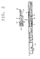
- Figure 2 is a side elevational view of the connector showing a cam mechanism assembled as part of the eject device.
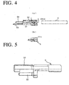
- Figure 3 shows an enlarged side elevational view of a slider.
- Card connector 1 is of generally rectangular shape and is provided with eject device IJ for card C to be inserted into a connector body B.
- Connector body B is composed of a housing 2 having a receiving slot 21 for receiving card C and a metal shell 3 for covering housing 2.
- Housing 2 is formed of insulation resin and has a bottom plate portion 2a ( Figure 2 ), right and left side wall portions 22 and 23, and a terminal mounting portion 24 provided on a front portion thereof.
- a plurality of terminal members 4 each having a contact portion 41 adapted to contact corresponding contacts (not shown) on card C are assembled into terminal mounting portion 24.
- Metal shell 3 is formed by stamping and forming a thin metal plate, and has an upper portion 31 and right and left plate portions 32 and 33.
- Eject device IJ includes: a slider 5 which moves in a sliding direction in response to the insertion of card C and slides between a forward position or loading position of card C whereat the terminal members are not in contact with the corresponding card contacts, and a back position or insertion position of card C, whereat the terminal member are in contact with the corresponding card contacts; a coil spring 6 for biasing the slider to the back position of the card; and a cam mechanism 7 for guiding and defining the sliding operation of the slider.
- Cam mechanism 7 is provided on a side surface of slider 5, and is provided with a first guide groove or cam groove 51 defining the forward position of slider 5, a second guide groove or cam groove 52 defining the back position of slider 5, and a pin member 8 for moving within guide grooves 51 and 52 and defining the sliding position of slider 5.
- Slider 5 is received within a recess portion 25 along a side portion of housing 2 and is covered by metal shell 3.
- slider 5 is provided with a guide mechanism for allowing the slider to continuously and smoothly slide during the sliding action.
- Slider 5 is provided with a body portion 50 slidably mounted relative to the housing and a guide post portion 53 extending from body portion 50 in the sliding direction.
- the guide mechanism includes a guide groove 26 ( Figure 2 ) in housing 2 extending in the sliding direction of slider 5 and a projection 54 provided in guide post portion 53 for movement along guide groove 26.
- Guide post portion 53 is close to a side surface of slider 5, opposite the side surface of first and second guide grooves 51 and 52.
- slider 5 further includes a cylindrical projection 55 for inserting into and holding one end of coil spring 6.
- This cylindrical projection projects in the sliding direction of slider 5. Accordingly, coil spring 6 is held in a coaxial manner.
- a rear surface of slider 5 is formed into an abutment surface 56 perpendicular to the sliding direction of slider 5 so that a forward end Cl of card C is brought into abutting contact with abutment surface 56.
- Side portion 32 of metal shell 3 is provided with a spring portion 32a for biasing a free end of pin member 8 when it is introduced into guide grooves 51 and 52 and prevents the free end portion from being pulled out.
- the spring portion 32a is formed inwardly from a portion of side portion 32 of metal shell 3.
- First guide groove 51 and second guide groove 52 are provided in one side surface of slider 5 and correspond to a forward passage LI and a return passage L2 as indicated by the dotted and dashed line in Figure 3 .
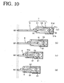
- Free end of pin member 8 is formed into an L-shape and is provided at its end with an engagement shaft portion 81 that moves within the guide grooves to define the motion of the slider (see Fig 10 ).
- Engagement shaft portion 81 is introduced into a start portion 51a of guide groove 51 at the back position of slider 5.
- a proximal end of pin member 8 is also formed into an L-shape to form a pivot shaft portion 82 relative to housing 2 and pivot shaft portion 82 is supported in housing 2 such that the free end of pin member 8 moves within each guide groove 51, 52 relative to pivot shaft portion 82.
- Figure 10(a) shows the initial condition or the back position of card C where the card is not inserted.
- the end portion Cl of card C is brought into abutment with vertical abutment surface 56 of slider 5 so that slider 5 is slidingly moved forward (toward the left in Figures 10 through 13 ).
- coil spring 6 is compressed.
- engagement shaft portion 81 of pin member 8 is prevented from moving toward second guide groove 52 by the presence of a stepped surface 5a (see Figure 3 ) so that it remains within first guide groove 51 ( Figure 10(b) ).
- engagement shaft portion 81 passes through first groove 51 and is brought into abutment with rear end recess portion 51b as shown in Figures 10(c) to 11(f) . Simultaneously, engagement shaft portion 81 moves through return-preventing stepped surfaces 5b and 5c (ref. Figure 3 ). During this time, the contacts of card C and contact portions 41 of the connector remain in electrical contact with each other.
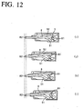
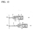
- slider 5 When the pushing force applied to card C stops, slider 5 is pushed back by the force of coil spring 6 to eject card C. At this time, engagement shaft portion 81 moves through second guide groove 52 and passes through stepped surfaces 5d and 5a ( Figure 3 ) to return to the initial position 51a (see Figures 12(l) to 13(m) ).
- engagement shaft portion 81 of pin member 8 moves through forward passage LI along first guide groove 51 and return passage L2 along second guide groove 52 so that insertion and ejection of card C is performed by a simple double push or "push-push" operation.
- connector body B can be made in a simple rectangular shape that substantially corresponds to the shape of card C. Accordingly, in addition to being thin, the design allows the connector to be miniaturized horizontally such that the area occupied on an underlying substrate is reduced.
- guide post portion 53 of slider 5 is provided close to the side surface, opposite the surface of the first and second guide grooves such that the force applied to the first and second guide grooves and the force applied to guide post 53 are balanced when the cam mechanism operates, therefore providing a smoother movement of slider 5.
- the card connector according to the present invention provides a compact and thin size connector that maintains smooth and continuous movement of the cam mechanism to enhance the operationability thereof.
Landscapes
- Engineering & Computer Science (AREA)
- Physics & Mathematics (AREA)
- General Physics & Mathematics (AREA)
- Theoretical Computer Science (AREA)
- Computer Hardware Design (AREA)
- Microelectronics & Electronic Packaging (AREA)
- Artificial Intelligence (AREA)
- Computer Vision & Pattern Recognition (AREA)
- Coupling Device And Connection With Printed Circuit (AREA)
- Details Of Connecting Devices For Male And Female Coupling (AREA)
Claims (7)
- Kartenverbinder (1) zur Aufnahme einer Karte (C) mit integrierter Schaltung, umfassend:einen Verbinderkörper (B), der ein Gehäuse (2) mit einem Aufnahmeschlitz (21) zur Aufnahme der Karte sowie eine Mehrzahl von Anschlusskontakten (4), die in diesem montiert sind, um entsprechende Kontakte auf der Karte (C) zu kontaktieren, umfasst;eine Metall ummantelung (3) zum Abdecken eines wesentlichen Teils des Gehäuses (2);eine Auswurfeinrichtung (IJ), welche umfasst:einen Schieber (5), der beweglich an dem Gehäuse (2) gelagert ist und an der Schaltungskarte (C) in Anlage gebracht werden kann, und zwar zur Bewegung mit dieser zwischen einem vorderen Kanal (L1), bei welchem die Kontakte der Karte (C) nicht die Anschlusskontakte (4) kontaktieren, und einer Einfügungsstellung (51c), in welcher die Kontakte der Karte (C) sich in Kontakt mit den Anschlusskontakten (4) befinden;eine Schraubenfeder (6) zum Bewegen des Schiebers (5) in Richtung der Einfügungsstellung (51c), wenn der Auswurfmechanismus (IJ) betätigt wird; undein Kurvengetriebe (7) zum Definieren der relativen Stellung des Schiebers (5),wobei das Kurvengetriebe (7) an einer seitlichen Oberfläche des Schiebers (5) vorgesehen ist und eine erste Führungsnut (51), welche den vorderen Kanal (L1) des Schiebers (5) definiert, und eine V-förmige Übergangsnut (51b, 51c, 51d) umfaßt welche die Einfügungsstellung (51c) des Schiebers (5) definiert und die erste Führungsnut (51) mit einer zweiten Führungsnut (52) verbindet, welche einen Rückführkanal (L2) für den Schieber (5) definiert; undein Stiftelement (8) mit einem freien Ende mit einem Schaftabschnitt (81) zur Bewegung in den Führungsnuten (51, 51b, 51c, 51d, 52), welche die Schiebestellung des Schiebers definieren, wobei der Schieber in einer Ausnehmung (25) entlang eines Seitenabschnitts des Gehäuses aufgenommen ist und durch die Metallummantelung abgedeckt ist;gekennzeichnet durcheinen Federabschnitt, der integral mit einem Seitenabschnitt (33) der Metallummantelung (3) ausgebildet ist, um das freie Ende des Stiftelements (8) in die Führungsnuten (51, 51b, 51c, 51d, 52) des Kurvengetriebe (7) zu drücken.
- Kartenverbinder nach Anspruch 1, bei welchem die Ummantelung (3) aus dünnem Metallplattenmäterial gestanzt und geformt ist und der Federabschnitt aus einem Abschnitt des Seitenteils (33) der Metallummantelung (3) nach innen geformt ist.
- Kartenverbinder nach Anspruch 1, bei welchem der Schieber (5) beweglich an einer Seite des Gehäuses (2) gelagert ist.
- Kartenverbinder nach Anspruch 1, welcher ferner einen Führungsmechanismus (53, 54, 26) umfasst, um ein Verschieben des Schiebers (5) in dem Gehäuse (2) des Verbinderkörpers (B) zu ermöglichen.
- Kartenverbinder nach Anspruch 4, bei welchem der Schieber einen Körperabschnitt (50) umfasst, der in Bezug auf das Gehäuse (2) verschiebbar gelagert ist, und wobei sich ein Führungszapfenabschnitt (53) in einer Verschiebungsrichtung des Schiebers (5) von dem Körperabschnitt (50) hinweg erstreckt, wobei der Führungsmechanismus (53, 54, 26) eine Führungsnut (26), die sich in der Verschiebungsrichtung des Schiebers (5) erstreckt, sowie einen Vorsprung (54), der an dem Führungszapfenabschnitt (53) zur Bewegung entlang der Führungsnut (26) vorgesehen ist, umfasst.
- Kartenverbinder nach Anspruch 5, bei welchem der Führungszapfenabschnitt (53) sich in der Nähe einer seitlichen Oberfläche des Schiebers (5) entgegengesetzt zu der seitlichen Oberfläche, an welcher die erste und die zweite Führungsnut (51, 52) ausgebildet sind, befindet.
- Kartenverbinder nach Anspruch 5, bei welchem der Schieber (5) ferner einen zylindrischen Vorsprung (50) umfasst, der von dem Körperabschnitt (55) vorsteht, und zwar zum Einfügen in ein Ende der Schraubenfeder und zum Halten dieser.
Applications Claiming Priority (2)
| Application Number | Priority Date | Filing Date | Title |
|---|---|---|---|
| JP2000066699 | 2000-03-10 | ||
| JP2000066699A JP4365977B2 (ja) | 2000-03-10 | 2000-03-10 | カード用コネクタ |
Publications (3)
| Publication Number | Publication Date |
|---|---|
| EP1132860A2 EP1132860A2 (de) | 2001-09-12 |
| EP1132860A3 EP1132860A3 (de) | 2001-10-10 |
| EP1132860B1 true EP1132860B1 (de) | 2009-06-17 |
Family
ID=18586017
Family Applications (1)
| Application Number | Title | Priority Date | Filing Date |
|---|---|---|---|
| EP01105957A Expired - Lifetime EP1132860B1 (de) | 2000-03-10 | 2001-03-09 | Leiterplattenverbinder mit Auswerfmechanismus |
Country Status (7)
| Country | Link |
|---|---|
| US (1) | US6520784B2 (de) |
| EP (1) | EP1132860B1 (de) |
| JP (1) | JP4365977B2 (de) |
| KR (1) | KR100414847B1 (de) |
| CN (1) | CN1313658A (de) |
| DE (1) | DE60138974D1 (de) |
| TW (1) | TW539288U (de) |
Families Citing this family (29)
| Publication number | Priority date | Publication date | Assignee | Title |
|---|---|---|---|---|
| JP3435384B2 (ja) | 2000-04-10 | 2003-08-11 | Smk株式会社 | メモリーカード用コネクタ |
| US6739890B2 (en) * | 2000-04-12 | 2004-05-25 | Molex Incorporated | Card connector assembly with improved ejection device |
| US6942505B2 (en) * | 2001-06-26 | 2005-09-13 | Molex Incorporated | Card connector |
| JP4028231B2 (ja) * | 2001-12-28 | 2007-12-26 | 日本圧着端子製造株式会社 | カード用コネクタのエジェクト機構 |
| JP4404545B2 (ja) * | 2002-12-27 | 2010-01-27 | ホシデン株式会社 | カードコネクタ |
| TWM241838U (en) * | 2003-02-24 | 2004-08-21 | Tai Sol Electronics Co Ltd | Card connector with card ejecting function |
| JP4168817B2 (ja) | 2003-04-23 | 2008-10-22 | モレックス インコーポレーテッド | カード用コネクタ |
| JP4393840B2 (ja) * | 2003-10-31 | 2010-01-06 | モレックス インコーポレイテド | カード用コネクタおよびプッシュプッシュ式のイジェクト機構 |
| JP3841353B2 (ja) * | 2003-12-26 | 2006-11-01 | 日本航空電子工業株式会社 | カード用コネクタ |
| CN101599582B (zh) * | 2004-03-18 | 2011-11-09 | 山一电机株式会社 | Ic卡用连接器 |
| CN100426594C (zh) | 2004-05-12 | 2008-10-15 | 美国莫列斯股份有限公司 | 电子卡连接器 |
| KR100663486B1 (ko) * | 2004-06-24 | 2007-01-02 | 삼성전자주식회사 | 휴대 단말기의 인터페이스 커넥터 커버 개폐장치 |
| US7008245B1 (en) * | 2004-11-17 | 2006-03-07 | L & K Precision Technology Co., Ltd. | Card connector |
| JP4799871B2 (ja) * | 2005-01-13 | 2011-10-26 | タイコエレクトロニクスジャパン合同会社 | カードコネクタ |
| US7004771B1 (en) * | 2005-03-14 | 2006-02-28 | Super Link Electronics Co., Ltd. | Electronic card connector capable of driving both sides of an electronic card to extract the electronic card |
| CN2831503Y (zh) * | 2005-08-15 | 2006-10-25 | 富士康(昆山)电脑接插件有限公司 | 记忆卡连接器 |
| CN100481639C (zh) * | 2005-12-21 | 2009-04-22 | 富士康(昆山)电脑接插件有限公司 | 卡连接器 |
| CN2914394Y (zh) * | 2006-03-22 | 2007-06-20 | 上海莫仕连接器有限公司 | 卡连接器的退卡机构 |
| CN201069835Y (zh) * | 2007-04-11 | 2008-06-04 | 富士康(昆山)电脑接插件有限公司 | 电子卡连接器 |
| TWI369033B (en) * | 2007-10-08 | 2012-07-21 | Hon Hai Prec Ind Co Ltd | Electrical card connector |
| TWI376686B (en) * | 2008-06-10 | 2012-11-11 | Pegatron Corp | Detachable drawer structure |
| CN201263146Y (zh) | 2008-09-04 | 2009-06-24 | 深圳华为通信技术有限公司 | 无线数据卡以及电子设备 |
| KR101135860B1 (ko) * | 2010-09-02 | 2012-06-05 | 한국몰렉스 주식회사 | 메모리 카드 소켓 및 그 메모리 카드 소켓의 하트 캠 |
| US8109773B1 (en) * | 2011-01-13 | 2012-02-07 | Hon Hai Precision Ind. Co., Ltd. | Multi-function card connector |
| TWI552454B (zh) * | 2015-03-25 | 2016-10-01 | 威剛科技股份有限公司 | 按壓式隨身存儲裝置 |
| JP1552813S (de) * | 2015-11-04 | 2016-06-27 | ||
| JP1552814S (de) * | 2015-11-04 | 2016-06-27 | ||
| CN109994857B (zh) * | 2019-04-10 | 2021-03-09 | 维沃移动通信有限公司 | 终端设备 |
| CN114251030B (zh) * | 2020-09-22 | 2023-01-31 | 观致汽车有限公司 | 滑动机构和具有其的隐藏式把手 |
Family Cites Families (22)
| Publication number | Priority date | Publication date | Assignee | Title |
|---|---|---|---|---|
| JPS6475983A (en) | 1987-09-18 | 1989-03-22 | Nissan Motor | Side wind sensor for vehicle |
| JPH01150387A (ja) | 1987-12-07 | 1989-06-13 | Matsushita Electric Works Ltd | プリント配線板 |
| JPH0418235Y2 (de) * | 1988-04-08 | 1992-04-23 | ||
| JP2541694Y2 (ja) * | 1991-12-27 | 1997-07-16 | ケル株式会社 | 抜出機構付きメモリーカード用コネクタ |
| JP3860230B2 (ja) * | 1993-11-19 | 2006-12-20 | バーグ・テクノロジー・インコーポレーテッド | データ処理媒体用コネクタ及びデータ処理媒体係止機構 |
| JP3076498B2 (ja) | 1994-09-27 | 2000-08-14 | ヒロセ電機株式会社 | Pcカード用電気コネクタ |
| JP3262491B2 (ja) | 1996-02-29 | 2002-03-04 | ヒロセ電機株式会社 | カード用電気コネクタ |
| US5818691A (en) * | 1997-01-21 | 1998-10-06 | Dell Usa, L.P. | Portable computer docking system with push to engage and push to disengage connection module |
| JP2887865B2 (ja) | 1997-06-02 | 1999-05-10 | アルプス電気株式会社 | コネクタ装置 |
| TW377909U (en) | 1997-07-15 | 1999-12-21 | Hon Hai Prec Ind Co Ltd | Electronic card connector |
| JP2887866B2 (ja) | 1997-07-29 | 1999-05-10 | アルプス電気株式会社 | Icカード用コネクタ装置 |
| JP2839242B1 (ja) | 1997-09-19 | 1998-12-16 | アルプス電気株式会社 | Icカード用コネクタ装置 |
| US6059587A (en) | 1997-10-02 | 2000-05-09 | Hon Hai Precision Ind. Co., Ltd. | Card connector |
| JP3483450B2 (ja) | 1998-01-26 | 2004-01-06 | アルプス電気株式会社 | Icカード用コネクタ装置 |
| JP3483449B2 (ja) | 1998-01-26 | 2004-01-06 | アルプス電気株式会社 | Icカード用コネクタ装置 |
| JP3297639B2 (ja) | 1998-01-28 | 2002-07-02 | ヒロセ電機株式会社 | カード用電気コネクタ |
| JP3483451B2 (ja) | 1998-01-28 | 2004-01-06 | アルプス電気株式会社 | Icカード用コネクタ装置 |
| JP3673395B2 (ja) | 1998-04-10 | 2005-07-20 | アルプス電気株式会社 | コネクタ装置 |
| JP3701792B2 (ja) | 1998-04-10 | 2005-10-05 | アルプス電気株式会社 | コネクタ装置 |
| JP3556090B2 (ja) | 1998-05-01 | 2004-08-18 | アルプス電気株式会社 | Icカード用コネクタ装置 |
| TW392950U (en) | 1998-12-31 | 2000-06-01 | Hon Hai Prec Ind Co Ltd | Improved connector structure for electronic card |
| TW456606U (en) | 1999-07-02 | 2001-09-21 | Hon Hai Prec Ind Co Ltd | Card ejecting mechanism of electronic card connector |
-
2000
- 2000-03-10 JP JP2000066699A patent/JP4365977B2/ja not_active Expired - Fee Related
-
2001
- 2001-03-09 EP EP01105957A patent/EP1132860B1/de not_active Expired - Lifetime
- 2001-03-09 DE DE60138974T patent/DE60138974D1/de not_active Expired - Fee Related
- 2001-03-09 CN CN01117326A patent/CN1313658A/zh active Pending
- 2001-03-10 KR KR10-2001-0012457A patent/KR100414847B1/ko not_active Expired - Fee Related
- 2001-03-12 US US09/804,444 patent/US6520784B2/en not_active Expired - Fee Related
- 2001-03-20 TW TW090203538U patent/TW539288U/zh not_active IP Right Cessation
Also Published As
| Publication number | Publication date |
|---|---|
| EP1132860A3 (de) | 2001-10-10 |
| KR20010088449A (ko) | 2001-09-26 |
| CN1313658A (zh) | 2001-09-19 |
| JP4365977B2 (ja) | 2009-11-18 |
| KR100414847B1 (ko) | 2004-01-13 |
| US20010031571A1 (en) | 2001-10-18 |
| JP2001257029A (ja) | 2001-09-21 |
| US6520784B2 (en) | 2003-02-18 |
| TW539288U (en) | 2003-06-21 |
| DE60138974D1 (de) | 2009-07-30 |
| EP1132860A2 (de) | 2001-09-12 |
Similar Documents
| Publication | Publication Date | Title |
|---|---|---|
| EP1132860B1 (de) | Leiterplattenverbinder mit Auswerfmechanismus | |
| US7815449B2 (en) | Memory card connector | |
| JP3429267B2 (ja) | カードコネクタ | |
| US6609919B2 (en) | Card connector | |
| US6814596B2 (en) | Card connector having low profile and vision indicator | |
| US6875033B2 (en) | Card connector | |
| US6592385B1 (en) | Card ejection mechanism for electronic card connector | |
| EP1678662B1 (de) | Speicherkartenverbinder mit kartenauswurfmechanismus | |
| US6839431B2 (en) | Card connector | |
| US6790061B1 (en) | Two-stage ejection mechanism of card connector | |
| US6554627B1 (en) | Electronic card connector and method for assembling same | |
| US6685490B1 (en) | Electrical card connector | |
| US6802448B2 (en) | Compact smart card reader with ejector | |
| US8770995B2 (en) | Card connector | |
| JP3965282B2 (ja) | ロック装置付きカードコネクタ | |
| WO2004095362A1 (en) | Memory card connector | |
| CN100442607C (zh) | 卡片用连接器 | |
| US7654836B2 (en) | Card connector | |
| EP1775802A1 (de) | IC-Kartenverbinder |
Legal Events
| Date | Code | Title | Description |
|---|---|---|---|
| PUAI | Public reference made under article 153(3) epc to a published international application that has entered the european phase |
Free format text: ORIGINAL CODE: 0009012 |
|
| PUAL | Search report despatched |
Free format text: ORIGINAL CODE: 0009013 |
|
| AK | Designated contracting states |
Kind code of ref document: A2 Designated state(s): AT BE CH CY DE DK ES FI FR GB GR IE IT LI LU MC NL PT SE TR Kind code of ref document: A2 Designated state(s): DE FR GB IE |
|
| AX | Request for extension of the european patent |
Free format text: AL;LT;LV;MK;RO;SI |
|
| AK | Designated contracting states |
Kind code of ref document: A3 Designated state(s): AT BE CH CY DE DK ES FI FR GB GR IE IT LI LU MC NL PT SE TR |
|
| AX | Request for extension of the european patent |
Free format text: AL;LT;LV;MK;RO;SI |
|
| RIC1 | Information provided on ipc code assigned before grant |
Free format text: 7G 06K 7/00 A, 7G 06K 13/08 B |
|
| 17P | Request for examination filed |
Effective date: 20020330 |
|
| AKX | Designation fees paid |
Free format text: DE FR GB IE |
|
| APBN | Date of receipt of notice of appeal recorded |
Free format text: ORIGINAL CODE: EPIDOSNNOA2E |
|
| APBR | Date of receipt of statement of grounds of appeal recorded |
Free format text: ORIGINAL CODE: EPIDOSNNOA3E |
|
| APBV | Interlocutory revision of appeal recorded |
Free format text: ORIGINAL CODE: EPIDOSNIRAPE |
|
| GRAP | Despatch of communication of intention to grant a patent |
Free format text: ORIGINAL CODE: EPIDOSNIGR1 |
|
| GRAS | Grant fee paid |
Free format text: ORIGINAL CODE: EPIDOSNIGR3 |
|
| GRAA | (expected) grant |
Free format text: ORIGINAL CODE: 0009210 |
|
| AK | Designated contracting states |
Kind code of ref document: B1 Designated state(s): DE FR GB IE |
|
| REG | Reference to a national code |
Ref country code: GB Ref legal event code: FG4D |
|
| REG | Reference to a national code |
Ref country code: IE Ref legal event code: FG4D |
|
| REF | Corresponds to: |
Ref document number: 60138974 Country of ref document: DE Date of ref document: 20090730 Kind code of ref document: P |
|
| PLBE | No opposition filed within time limit |
Free format text: ORIGINAL CODE: 0009261 |
|
| STAA | Information on the status of an ep patent application or granted ep patent |
Free format text: STATUS: NO OPPOSITION FILED WITHIN TIME LIMIT |
|
| 26N | No opposition filed |
Effective date: 20100318 |
|
| GBPC | Gb: european patent ceased through non-payment of renewal fee |
Effective date: 20100309 |
|
| REG | Reference to a national code |
Ref country code: FR Ref legal event code: ST Effective date: 20101130 |
|
| PG25 | Lapsed in a contracting state [announced via postgrant information from national office to epo] |
Ref country code: IE Free format text: LAPSE BECAUSE OF NON-PAYMENT OF DUE FEES Effective date: 20100309 Ref country code: FR Free format text: LAPSE BECAUSE OF NON-PAYMENT OF DUE FEES Effective date: 20100331 |
|
| PG25 | Lapsed in a contracting state [announced via postgrant information from national office to epo] |
Ref country code: DE Free format text: LAPSE BECAUSE OF NON-PAYMENT OF DUE FEES Effective date: 20101001 |
|
| PG25 | Lapsed in a contracting state [announced via postgrant information from national office to epo] |
Ref country code: GB Free format text: LAPSE BECAUSE OF NON-PAYMENT OF DUE FEES Effective date: 20100309 |