EP1132719B1 - Reflexions-Messteilung - Google Patents
Reflexions-Messteilung Download PDFInfo
- Publication number
- EP1132719B1 EP1132719B1 EP01104953A EP01104953A EP1132719B1 EP 1132719 B1 EP1132719 B1 EP 1132719B1 EP 01104953 A EP01104953 A EP 01104953A EP 01104953 A EP01104953 A EP 01104953A EP 1132719 B1 EP1132719 B1 EP 1132719B1
- Authority
- EP
- European Patent Office
- Prior art keywords
- graduated
- reflective
- layer
- measuring scale
- scale according
- Prior art date
- Legal status (The legal status is an assumption and is not a legal conclusion. Google has not performed a legal analysis and makes no representation as to the accuracy of the status listed.)
- Expired - Lifetime
Links
- 239000000758 substrate Substances 0.000 claims description 27
- 239000000463 material Substances 0.000 claims description 21
- 239000006096 absorbing agent Substances 0.000 claims description 14
- VYPSYNLAJGMNEJ-UHFFFAOYSA-N Silicium dioxide Chemical compound O=[Si]=O VYPSYNLAJGMNEJ-UHFFFAOYSA-N 0.000 claims description 6
- XUIMIQQOPSSXEZ-UHFFFAOYSA-N Silicon Chemical compound [Si] XUIMIQQOPSSXEZ-UHFFFAOYSA-N 0.000 claims description 6
- 230000005855 radiation Effects 0.000 claims description 6
- 229910052710 silicon Inorganic materials 0.000 claims description 6
- 239000010703 silicon Substances 0.000 claims description 6
- 229910000831 Steel Inorganic materials 0.000 claims description 5
- 239000010959 steel Substances 0.000 claims description 5
- 238000010521 absorption reaction Methods 0.000 claims description 4
- 229910044991 metal oxide Inorganic materials 0.000 claims description 3
- 150000004706 metal oxides Chemical class 0.000 claims description 3
- 239000000377 silicon dioxide Substances 0.000 claims description 3
- 230000002745 absorbent Effects 0.000 claims description 2
- 239000002250 absorbent Substances 0.000 claims description 2
- PNEYBMLMFCGWSK-UHFFFAOYSA-N aluminium oxide Inorganic materials [O-2].[O-2].[O-2].[Al+3].[Al+3] PNEYBMLMFCGWSK-UHFFFAOYSA-N 0.000 claims 1
- 229910052681 coesite Inorganic materials 0.000 claims 1
- 229910052593 corundum Inorganic materials 0.000 claims 1
- 229910052906 cristobalite Inorganic materials 0.000 claims 1
- 229910052682 stishovite Inorganic materials 0.000 claims 1
- 229910052905 tridymite Inorganic materials 0.000 claims 1
- 229910001845 yogo sapphire Inorganic materials 0.000 claims 1
- 238000005259 measurement Methods 0.000 description 27
- 238000000034 method Methods 0.000 description 17
- 229920002120 photoresistant polymer Polymers 0.000 description 7
- 238000002310 reflectometry Methods 0.000 description 7
- 238000004519 manufacturing process Methods 0.000 description 6
- VYZAMTAEIAYCRO-UHFFFAOYSA-N Chromium Chemical compound [Cr] VYZAMTAEIAYCRO-UHFFFAOYSA-N 0.000 description 5
- 239000011651 chromium Substances 0.000 description 5
- 229910052782 aluminium Inorganic materials 0.000 description 4
- XAGFODPZIPBFFR-UHFFFAOYSA-N aluminium Chemical compound [Al] XAGFODPZIPBFFR-UHFFFAOYSA-N 0.000 description 4
- 238000011109 contamination Methods 0.000 description 4
- 230000003287 optical effect Effects 0.000 description 4
- 229910004298 SiO 2 Inorganic materials 0.000 description 3
- 229910052804 chromium Inorganic materials 0.000 description 3
- 230000000694 effects Effects 0.000 description 3
- BASFCYQUMIYNBI-UHFFFAOYSA-N platinum Chemical compound [Pt] BASFCYQUMIYNBI-UHFFFAOYSA-N 0.000 description 3
- 238000005070 sampling Methods 0.000 description 3
- 239000011248 coating agent Substances 0.000 description 2
- 238000000576 coating method Methods 0.000 description 2
- 230000001419 dependent effect Effects 0.000 description 2
- 238000000206 photolithography Methods 0.000 description 2
- 238000005240 physical vapour deposition Methods 0.000 description 2
- 235000012239 silicon dioxide Nutrition 0.000 description 2
- 238000004544 sputter deposition Methods 0.000 description 2
- 239000010936 titanium Substances 0.000 description 2
- 229910018072 Al 2 O 3 Inorganic materials 0.000 description 1
- 229910021569 Manganese fluoride Inorganic materials 0.000 description 1
- ZOKXTWBITQBERF-UHFFFAOYSA-N Molybdenum Chemical compound [Mo] ZOKXTWBITQBERF-UHFFFAOYSA-N 0.000 description 1
- RTAQQCXQSZGOHL-UHFFFAOYSA-N Titanium Chemical compound [Ti] RTAQQCXQSZGOHL-UHFFFAOYSA-N 0.000 description 1
- WGLPBDUCMAPZCE-UHFFFAOYSA-N Trioxochromium Chemical compound O=[Cr](=O)=O WGLPBDUCMAPZCE-UHFFFAOYSA-N 0.000 description 1
- 238000005299 abrasion Methods 0.000 description 1
- 229910000423 chromium oxide Inorganic materials 0.000 description 1
- 239000002826 coolant Substances 0.000 description 1
- CTNMMTCXUUFYAP-UHFFFAOYSA-L difluoromanganese Chemical compound F[Mn]F CTNMMTCXUUFYAP-UHFFFAOYSA-L 0.000 description 1
- 238000011156 evaluation Methods 0.000 description 1
- PCHJSUWPFVWCPO-UHFFFAOYSA-N gold Chemical compound [Au] PCHJSUWPFVWCPO-UHFFFAOYSA-N 0.000 description 1
- 239000010931 gold Substances 0.000 description 1
- 229910052737 gold Inorganic materials 0.000 description 1
- 239000000314 lubricant Substances 0.000 description 1
- 229910052751 metal Inorganic materials 0.000 description 1
- 239000002184 metal Substances 0.000 description 1
- 229910052750 molybdenum Inorganic materials 0.000 description 1
- 239000011733 molybdenum Substances 0.000 description 1
- 230000005693 optoelectronics Effects 0.000 description 1
- TWNQGVIAIRXVLR-UHFFFAOYSA-N oxo(oxoalumanyloxy)alumane Chemical compound O=[Al]O[Al]=O TWNQGVIAIRXVLR-UHFFFAOYSA-N 0.000 description 1
- 238000005192 partition Methods 0.000 description 1
- 239000011295 pitch Substances 0.000 description 1
- 229910052697 platinum Inorganic materials 0.000 description 1
- 238000002360 preparation method Methods 0.000 description 1
- 230000035945 sensitivity Effects 0.000 description 1
- 229910001220 stainless steel Inorganic materials 0.000 description 1
- 238000010025 steaming Methods 0.000 description 1
- 229910052715 tantalum Inorganic materials 0.000 description 1
- GUVRBAGPIYLISA-UHFFFAOYSA-N tantalum atom Chemical compound [Ta] GUVRBAGPIYLISA-UHFFFAOYSA-N 0.000 description 1
- 229910052719 titanium Inorganic materials 0.000 description 1
- WFKWXMTUELFFGS-UHFFFAOYSA-N tungsten Chemical compound [W] WFKWXMTUELFFGS-UHFFFAOYSA-N 0.000 description 1
- 229910052721 tungsten Inorganic materials 0.000 description 1
- 239000010937 tungsten Substances 0.000 description 1
- 238000007740 vapor deposition Methods 0.000 description 1
Images

Classifications
-
- G—PHYSICS
- G02—OPTICS
- G02B—OPTICAL ELEMENTS, SYSTEMS OR APPARATUS
- G02B5/00—Optical elements other than lenses
- G02B5/08—Mirrors
-
- G—PHYSICS
- G01—MEASURING; TESTING
- G01D—MEASURING NOT SPECIALLY ADAPTED FOR A SPECIFIC VARIABLE; ARRANGEMENTS FOR MEASURING TWO OR MORE VARIABLES NOT COVERED IN A SINGLE OTHER SUBCLASS; TARIFF METERING APPARATUS; MEASURING OR TESTING NOT OTHERWISE PROVIDED FOR
- G01D5/00—Mechanical means for transferring the output of a sensing member; Means for converting the output of a sensing member to another variable where the form or nature of the sensing member does not constrain the means for converting; Transducers not specially adapted for a specific variable
- G01D5/26—Mechanical means for transferring the output of a sensing member; Means for converting the output of a sensing member to another variable where the form or nature of the sensing member does not constrain the means for converting; Transducers not specially adapted for a specific variable characterised by optical transfer means, i.e. using infrared, visible, or ultraviolet light
- G01D5/32—Mechanical means for transferring the output of a sensing member; Means for converting the output of a sensing member to another variable where the form or nature of the sensing member does not constrain the means for converting; Transducers not specially adapted for a specific variable characterised by optical transfer means, i.e. using infrared, visible, or ultraviolet light with attenuation or whole or partial obturation of beams of light
- G01D5/34—Mechanical means for transferring the output of a sensing member; Means for converting the output of a sensing member to another variable where the form or nature of the sensing member does not constrain the means for converting; Transducers not specially adapted for a specific variable characterised by optical transfer means, i.e. using infrared, visible, or ultraviolet light with attenuation or whole or partial obturation of beams of light the beams of light being detected by photocells
- G01D5/347—Mechanical means for transferring the output of a sensing member; Means for converting the output of a sensing member to another variable where the form or nature of the sensing member does not constrain the means for converting; Transducers not specially adapted for a specific variable characterised by optical transfer means, i.e. using infrared, visible, or ultraviolet light with attenuation or whole or partial obturation of beams of light the beams of light being detected by photocells using displacement encoding scales
- G01D5/34707—Scales; Discs, e.g. fixation, fabrication, compensation
Definitions
- the present invention relates to a reflection measurement graduation.
- Optical incident-light position-measuring devices usually comprise a Reflection measuring graduation and a relatively movable scanning unit.
- a light source On the part of the scanning unit, a light source is usually arranged, the emits a light beam in the direction of the reflection measurement graduation. From there there is a return reflection in the direction of the scanning unit, where the shift-dependent modulated light bundles if necessary by one or more scanning divisions occurs and finally by an optoelectronic detector array is detected.
- the thus generated, shift-modulated Sampling signals are then transmitted via a downstream evaluation unit further processed.
- Known reflection measurement graduations that are used in these measuring devices usually consist of a carrier substrate on which alternating line portions with different reflection properties are arranged in the measuring direction.
- a full-surface coating with chromium steel carrier substrate can be provided on a steel carrier substrate a full-surface coating with chromium.
- absorbing or low-reflective subregions of chromium oxide Cr 2 O 3 are arranged on the chromium layer.
- the highly reflective subregions are formed by the exposed chrome subregions.
- Such reflection measurement pitches are subject to a number of requirements posed.
- u.a. the highest possible abrasion resistance, a high reflectivity in the highly reflective subregions, the greatest possible absorption in the low-reflecting Teü Hochen and to impart the lowest possible sensitivity to contamination.
- the above-explained variants of a reflection measurement graduation now turns out to be relatively sensitive to pollution. This reduces For example, when it comes to contamination with coolants or lubricants, the reflectivity of the highly reflective subregions, while the reflectivity in the slightly reflective subregions increases significantly. Overall results in the event of contamination, a significantly reduced degree of modulation of Scanning signals when this measurement division in an optical incident light position measuring device is used.
- EP 0 773 458 A1 also discloses an incident-light phase grating in which the different, each reflecting subregions one each different pahsenschiebende effect on the incident and then exercise reflected radiation.
- EP 0 497 742 A1 proposes an incident light measuring graduation, in the highly reflective aluminum and SiO 2 layer on a steel substrate be applied over the entire surface and in turn the low-reflective Chrome bars of the division structure.
- the object of the present invention is a reflection measurement graduation specify that is as insensitive to contamination as possible.
- the reflection measurement division according to the invention offers in comparison to Previous solutions have a number of advantages. So, for one thing ensured that even in the case of a possible pollution a high Degree of modulation of the sampling remains ensured if such Reflection measurement graduation in an optical incident-light position-measuring device is used. It is also a case of pollution both sufficiently high reflectivity in the highly reflective sub-areas as also a sufficiently high absorption in the low-reflective Subareas of the measurement division before.
- the reflection measurement graduation according to the invention is also distinguished by a high mechanical load capacity.
- a for the preparation of the inventive reflection measurement used method requires only a small number of Process steps; such is just a single structuring step necessary. Likewise, there are no procedurally complex processes when setting the required layer thicknesses.
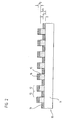
- Figure 1 is a plan view of a part of an inventively designed Reflection measurement division 10 shown.
- the reflection measuring graduation 10 formed as a linear incremental graduation, the alternately arranged in the x-direction of the first and second portions 12, 13, which in a track 15 on a support substrate 11th are arranged.
- the first portions 12 are highly reflective designed; the second portions 13 are designed to be slightly reflective.
- inventive design of the sections 12, 13 is to the following description in Figures 2 and 3a -3e referenced.
- the Subregions 12, 13 with different reflective properties respectively the identical geometric shape and consist of narrow Rectangles, the width b in the x direction and the length l in the y direction have. From the sum of the widths b of two subregions 12, 13 results yourself for the resolution of a corresponding incremental Position measuring device relevant graduation period TP.
- the direction indicated by x, along which the subregions 12, 13 arranged are, corresponds to the direction of measurement. Along this direction moves in a corresponding incident light position measuring a - Not shown - scanning relative to the reflection measurement division 10th
- the reflection measurement division according to the invention also alternatively be formed rotatory; it is natural too possible to design an absolutely coded measuring graduation according to the invention, in which the subregions 12, 13 different widths b in the x direction have etc.
- carrier substrate 11 of the reflection measuring graduation 10 is in this case polished Steel provided, which has a high reflectivity for the incident radiation having. Usual thicknesses of the carrier substrate 11 are in the range between 1mm and 15mm.
- carrier substrates 11 for example, other metallic reflectors made of titanium Ti, Tungsten W, molybdenum Mo, platinum Pt, tantalum Ta or chromium Cr.
- the low-reflection, second partial regions 13 of the reflection measuring graduation 10 according to the invention consist of an absorber layer 14 which is applied directly to the carrier substrate 11.
- the absorber layer 14 would also be weak absorbing metal oxides into consideration.
- the highly reflective, first portions 12 are according to the invention of several partial layers 15, 16 with different refractive indices, which are arranged one above the other on the carrier substrate 11 and as an interference filter Act.
- the highly reflective portions 12 of the reflection measurement graduation 10 are accordingly according to the invention as a dielectric reflection interference filter educated.
- the partial layer 15 arranged directly on the carrier substrate 11 is referred to below as the first partial layer 15, which has a refractive index n 1 .
- the uppermost sub-layer 16 arranged above is referred to below as the second sub-layer 16 and has the refractive index n 2 .
- the refractive index n 1 of the first sub-layer 15, which is arranged directly on the carrier substrate 11, is chosen to be significantly smaller than the refractive index n 2 of the second sub-layer 16 arranged above it in order to achieve the desired interference effect.
- silicon dioxide SiO 2 is selected as the material for the low-refractive, first partial layer 15.
- Aluminum oxide Al 2 O 3 or else manganese fluoride MgF 2 would also be considered as alternative materials for the first part-layer 15.
- silicon Si is selected, ie the identical material as for the absorber layer 14.
- the refractive index n 2 of the second partial layer 16 is preferably chosen to be greater than or equal to 2.2, ie n 2 ⁇ 2.2.
- the identical alternative materials come into consideration as for the absorber layer 14, ie, for example, weakly absorbing metal oxides.
- the inventive design ensures the highly reflective portions 12 a high mechanical strength.
- Reflection measurement division 10 results from the fact that for the absorber layer 14 and the second partial layer 16 identical Material is selected, in the present example silicon Si.
- identical Material is selected, in the present example silicon Si.
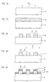
- FIG. 3 a shows how in a first step of the illustrated exemplary embodiment of the method on the carrier substrate 11 in the form of polished steel, a first partial layer is applied over a PVD method, eg vapor deposition or sputtering.
- a PVD method eg vapor deposition or sputtering.
- silicon dioxide SiO 2 is provided as explained above.
- the areal first sub-layer 15 is structured such that only in the first sub-areas 12, the first sub-layer 15 remains while in between lying second sub-areas 13, the first sub-layer 15 completely again Will get removed.
- the result of this structuring step is shown in FIG 3c.
- Such structuring is carried out by means of a conventional photolithography method, on this is not closer.
- a second partial layer 16 becomes uniform the first and second portions 12, 13 applied, wherein in the example According to FIG. 3d, silicon Si as the material of the second partial layer 16 is applied.
- a conventional PVD method is chosen, such as steaming or Sputtering.
- the materials for the different partial layers 15, 16 are selected with regard to their refractive indices n 1 , n 2 such that a dielectric reflection interference filter is formed in the region of the highly reflective first partial regions 13.
- the refractive index n 2 of the second partial layer 16 is in this case significantly greater than the refractive index n 1 of the first partial layer 15.
- the thicknesses d 1 , d 2 of the two partial layers 15, 16 are set as indicated above.
- FIG. 3e finally shows the finished reflection measurement graduation 10.
- the subsequent procedure instead of the process steps in FIGS. 3a and 3b, to to come to a structure, as shown in Figure 3c.
- This is in a first method step, the carrier substrate 11 over the entire surface coated with a photoresist.
- the photoresist is then over a Photolithography process is structured so that partial areas on the Carrier substrate 11 with photoresist and portions without photoresist result, which correspond to the subregions 12, 13 in Figure 3c. thereupon is the entire surface of the first sub-layer 15 on the support substrate 11 inclusive applied structured photoresist.
- the next process step will be then those subregions removed, in which those photoresist under the first sub-layer 15 is located, so that the structure according to Figure 3c results; then the procedure is as explained above.
Landscapes
- Physics & Mathematics (AREA)
- General Physics & Mathematics (AREA)
- Optics & Photonics (AREA)
- Optical Transform (AREA)
- Optical Elements Other Than Lenses (AREA)
- Length Measuring Devices By Optical Means (AREA)
Applications Claiming Priority (2)
| Application Number | Priority Date | Filing Date | Title |
|---|---|---|---|
| DE10011872A DE10011872A1 (de) | 2000-03-10 | 2000-03-10 | Reflexions-Messteilung und Verfahren zur Herstellung derselben |
| DE10011872 | 2000-03-10 |
Publications (2)
| Publication Number | Publication Date |
|---|---|
| EP1132719A1 EP1132719A1 (de) | 2001-09-12 |
| EP1132719B1 true EP1132719B1 (de) | 2005-06-01 |
Family
ID=7634333
Family Applications (1)
| Application Number | Title | Priority Date | Filing Date |
|---|---|---|---|
| EP01104953A Expired - Lifetime EP1132719B1 (de) | 2000-03-10 | 2001-03-01 | Reflexions-Messteilung |
Country Status (4)
| Country | Link |
|---|---|
| US (1) | US6671092B2 (enExample) |
| EP (1) | EP1132719B1 (enExample) |
| JP (1) | JP4545966B2 (enExample) |
| DE (2) | DE10011872A1 (enExample) |
Families Citing this family (12)
| Publication number | Priority date | Publication date | Assignee | Title |
|---|---|---|---|---|
| DE10150099A1 (de) * | 2001-10-11 | 2003-04-17 | Heidenhain Gmbh Dr Johannes | Verfahren zur Herstellung eines Maßstabes, sowie derart hergestellter Maßstab und eine Positionsmesseinrichtung |
| JP2004028862A (ja) * | 2002-06-27 | 2004-01-29 | Harmonic Drive Syst Ind Co Ltd | 投影型エンコーダ |
| US20040035012A1 (en) * | 2002-08-26 | 2004-02-26 | Moehnke Stephanie J. | Measuring device having symbols viewable in multiple orientations |
| US7256938B2 (en) * | 2004-03-17 | 2007-08-14 | General Atomics | Method for making large scale multilayer dielectric diffraction gratings on thick substrates using reactive ion etching |
| US7321467B2 (en) * | 2005-05-26 | 2008-01-22 | Macronix International Co., Ltd. | Anti-reflection coating layer and design method thereof |
| WO2008146409A1 (ja) * | 2007-06-01 | 2008-12-04 | Mitutoyo Corporation | 反射型エンコーダ、そのスケール、及び、スケールの製造方法 |
| AT509101B1 (de) * | 2009-11-18 | 2011-10-15 | Victor Vasiloiu | Induktive messeinrichtung für längen- und winkelerfassung |
| US20140071532A1 (en) * | 2010-12-16 | 2014-03-13 | Suzhou University | Color filter |
| US10317254B2 (en) * | 2014-03-27 | 2019-06-11 | Ams Sensors Singapore Pte. Ltd. | Optical encoder system |
| JP7140495B2 (ja) * | 2017-12-28 | 2022-09-21 | 株式会社ミツトヨ | スケールおよびその製造方法 |
| JP2021131312A (ja) * | 2020-02-20 | 2021-09-09 | 株式会社ミツトヨ | スケール |
| JP7574845B2 (ja) * | 2020-03-31 | 2024-10-29 | 大日本印刷株式会社 | エンコーダ用反射型光学式スケール及び反射型光学式エンコーダ |
Family Cites Families (12)
| Publication number | Priority date | Publication date | Assignee | Title |
|---|---|---|---|---|
| DE1279944B (de) * | 1965-09-15 | 1968-10-10 | Wenczler & Heidenhain | Messteilung |
| US4374612A (en) | 1980-07-25 | 1983-02-22 | Canon Kabushiki Kaisha | Mark indicating device for optical apparatus |
| US4286871A (en) * | 1980-08-11 | 1981-09-01 | Keuffel & Esser Company | Photogrammetric measuring system |
| JPS5875004A (ja) * | 1981-10-30 | 1983-05-06 | Mitsutoyo Mfg Co Ltd | 光電式変位検出装置の反射型スケ−ルの製造方法 |
| JPS60118912U (ja) | 1984-01-18 | 1985-08-12 | アルプス電気株式会社 | 反射型光学式ロ−タリエンコ−ダのコ−ドホイ−ル |
| JPS60161523A (ja) * | 1984-02-02 | 1985-08-23 | Mitsutoyo Mfg Co Ltd | 三次元測定機 |
| JPS60217361A (ja) * | 1984-04-13 | 1985-10-30 | Alps Electric Co Ltd | 光反射式コ−ド板 |
| JPS6145923A (ja) * | 1984-08-10 | 1986-03-06 | Aronshiya:Kk | 反射式ロ−タリ−エンコ−ダ−用回転デイスクの製作方法 |
| IT1245008B (it) * | 1991-01-25 | 1994-09-13 | Lamsweerde Edoardo Van | Elemento graduato per lettura ottica a riflessione e procedimento per la sua fabbricazione |
| JPH0933221A (ja) * | 1995-07-21 | 1997-02-07 | Mitsutoyo Corp | 測長スケール |
| DE59507969D1 (de) * | 1995-11-11 | 2000-04-13 | Heidenhain Gmbh Dr Johannes | Auflicht-Phasengitter |
| US6027815A (en) | 1996-11-06 | 2000-02-22 | Taiwan Semiconductor Manufacturing Company | Non-absorbing anti-reflective coated (ARC) reticle using thin dielectric films and method of forming reticle |
-
2000
- 2000-03-10 DE DE10011872A patent/DE10011872A1/de not_active Withdrawn
-
2001
- 2001-02-22 JP JP2001046694A patent/JP4545966B2/ja not_active Expired - Fee Related
- 2001-03-01 EP EP01104953A patent/EP1132719B1/de not_active Expired - Lifetime
- 2001-03-01 DE DE50106355T patent/DE50106355D1/de not_active Expired - Lifetime
- 2001-03-08 US US09/801,449 patent/US6671092B2/en not_active Expired - Fee Related
Also Published As
| Publication number | Publication date |
|---|---|
| JP4545966B2 (ja) | 2010-09-15 |
| JP2001296146A (ja) | 2001-10-26 |
| US6671092B2 (en) | 2003-12-30 |
| DE10011872A1 (de) | 2001-09-27 |
| DE50106355D1 (de) | 2005-07-07 |
| EP1132719A1 (de) | 2001-09-12 |
| US20010021485A1 (en) | 2001-09-13 |
Similar Documents
| Publication | Publication Date | Title |
|---|---|---|
| EP1132719B1 (de) | Reflexions-Messteilung | |
| DE3611852C2 (enExample) | ||
| EP2381280B1 (de) | IR-Neutralfilter mit einem für Infrarotstrahlung transparenten Substrat | |
| EP1081457B1 (de) | Optische Positionsmesseinrichtung | |
| DE19608978A1 (de) | Phasengitter und Verfahren zur Herstellung eines Phasengitters | |
| DE112011104918T5 (de) | Optischer Geber | |
| EP1436647B1 (de) | Verfahren zur herstellung eines massstabes, sowie derart hergestellter massstab und eine positionsmesseinrichtung | |
| DE3786318T2 (de) | Rotierender optischer kodierer. | |
| EP3260820A1 (de) | Optische positionsmesseinrichtung | |
| DE4303975A1 (de) | Teilungsträger | |
| DE3412958A1 (de) | Phasengitter | |
| EP0724168B1 (de) | Positionsmesseinrichtung mit Phasengitter und Herstellungsverfahren | |
| EP0763715B1 (de) | Vorrichtung zur Filterung von Oberwellen-Signalanteilen | |
| EP3150970A1 (de) | Optisches schichtsystem | |
| DE19937023A1 (de) | Reflexions-Maßverkörperung und Verfahren zur Herstellung einer Reflexions-Maßverkörperung | |
| EP2570780B1 (de) | Rotatorische Positionsmesseinrichtung | |
| EP0773458B1 (de) | Auflicht-Phasengitter | |
| DE102017213330A1 (de) | Abtastplatte für eine optische Positionsmesseinrichtung | |
| DE3503116C2 (enExample) | ||
| EP1801546A1 (de) | Informationsträger in einem Encoder | |
| WO2004010170A1 (de) | Optische positions- oder längenbestimmung | |
| DE102004002683A1 (de) | Optische Positions- oder Längenbestimmung | |
| EP4502544B1 (de) | Optische positionsmesseinrichtung | |
| EP4170291A1 (de) | Optische positionsmesseinrichtung | |
| DE4317834C2 (de) | Spektralempfindlicher optoelektrischer Detektor |
Legal Events
| Date | Code | Title | Description |
|---|---|---|---|
| PUAI | Public reference made under article 153(3) epc to a published international application that has entered the european phase |
Free format text: ORIGINAL CODE: 0009012 |
|
| AK | Designated contracting states |
Kind code of ref document: A1 Designated state(s): AT BE CH CY DE DK ES FI FR GB GR IE IT LI LU MC NL PT SE TR |
|
| AX | Request for extension of the european patent |
Free format text: AL;LT;LV;MK;RO;SI |
|
| 17P | Request for examination filed |
Effective date: 20020312 |
|
| AKX | Designation fees paid |
Free format text: AT BE CH CY DE DK ES FI FR GB GR IE IT LI LU MC NL PT SE TR |
|
| 17Q | First examination report despatched |
Effective date: 20040513 |
|
| GRAP | Despatch of communication of intention to grant a patent |
Free format text: ORIGINAL CODE: EPIDOSNIGR1 |
|
| RTI1 | Title (correction) |
Free format text: REFLECTIVE MEASURING SCALE |
|
| RTI1 | Title (correction) |
Free format text: REFLECTIVE MEASURING SCALE |
|
| GRAS | Grant fee paid |
Free format text: ORIGINAL CODE: EPIDOSNIGR3 |
|
| RBV | Designated contracting states (corrected) |
Designated state(s): CH DE FR GB IT LI |
|
| GRAA | (expected) grant |
Free format text: ORIGINAL CODE: 0009210 |
|
| AK | Designated contracting states |
Kind code of ref document: B1 Designated state(s): CH DE FR GB IT LI |
|
| REG | Reference to a national code |
Ref country code: GB Ref legal event code: FG4D Free format text: NOT ENGLISH |
|
| REG | Reference to a national code |
Ref country code: CH Ref legal event code: EP Ref country code: CH Ref legal event code: NV Representative=s name: TROESCH SCHEIDEGGER WERNER AG |
|
| GBT | Gb: translation of ep patent filed (gb section 77(6)(a)/1977) |
Effective date: 20050601 |
|
| REG | Reference to a national code |
Ref country code: IE Ref legal event code: FG4D Free format text: LANGUAGE OF EP DOCUMENT: GERMAN |
|
| REF | Corresponds to: |
Ref document number: 50106355 Country of ref document: DE Date of ref document: 20050707 Kind code of ref document: P |
|
| ET | Fr: translation filed | ||
| PLBE | No opposition filed within time limit |
Free format text: ORIGINAL CODE: 0009261 |
|
| STAA | Information on the status of an ep patent application or granted ep patent |
Free format text: STATUS: NO OPPOSITION FILED WITHIN TIME LIMIT |
|
| 26N | No opposition filed |
Effective date: 20060302 |
|
| PGFP | Annual fee paid to national office [announced via postgrant information from national office to epo] |
Ref country code: FR Payment date: 20110404 Year of fee payment: 11 Ref country code: CH Payment date: 20110324 Year of fee payment: 11 Ref country code: IT Payment date: 20110325 Year of fee payment: 11 |
|
| REG | Reference to a national code |
Ref country code: CH Ref legal event code: PL |
|
| REG | Reference to a national code |
Ref country code: FR Ref legal event code: ST Effective date: 20121130 |
|
| PG25 | Lapsed in a contracting state [announced via postgrant information from national office to epo] |
Ref country code: CH Free format text: LAPSE BECAUSE OF NON-PAYMENT OF DUE FEES Effective date: 20120331 Ref country code: FR Free format text: LAPSE BECAUSE OF NON-PAYMENT OF DUE FEES Effective date: 20120402 Ref country code: LI Free format text: LAPSE BECAUSE OF NON-PAYMENT OF DUE FEES Effective date: 20120331 |
|
| PG25 | Lapsed in a contracting state [announced via postgrant information from national office to epo] |
Ref country code: IT Free format text: LAPSE BECAUSE OF NON-PAYMENT OF DUE FEES Effective date: 20120301 |
|
| PGFP | Annual fee paid to national office [announced via postgrant information from national office to epo] |
Ref country code: GB Payment date: 20160321 Year of fee payment: 16 |
|
| GBPC | Gb: european patent ceased through non-payment of renewal fee |
Effective date: 20170301 |
|
| PG25 | Lapsed in a contracting state [announced via postgrant information from national office to epo] |
Ref country code: GB Free format text: LAPSE BECAUSE OF NON-PAYMENT OF DUE FEES Effective date: 20170301 |
|
| PGFP | Annual fee paid to national office [announced via postgrant information from national office to epo] |
Ref country code: DE Payment date: 20180322 Year of fee payment: 18 |
|
| REG | Reference to a national code |
Ref country code: DE Ref legal event code: R119 Ref document number: 50106355 Country of ref document: DE |
|
| PG25 | Lapsed in a contracting state [announced via postgrant information from national office to epo] |
Ref country code: DE Free format text: LAPSE BECAUSE OF NON-PAYMENT OF DUE FEES Effective date: 20191001 |