EP1130707A2 - Gehäuse für optische Halbleitervorrichtung - Google Patents
Gehäuse für optische Halbleitervorrichtung Download PDFInfo
- Publication number
- EP1130707A2 EP1130707A2 EP01300636A EP01300636A EP1130707A2 EP 1130707 A2 EP1130707 A2 EP 1130707A2 EP 01300636 A EP01300636 A EP 01300636A EP 01300636 A EP01300636 A EP 01300636A EP 1130707 A2 EP1130707 A2 EP 1130707A2
- Authority
- EP
- European Patent Office
- Prior art keywords
- fiber
- optical
- light
- assembly
- termination
- Prior art date
- Legal status (The legal status is an assumption and is not a legal conclusion. Google has not performed a legal analysis and makes no representation as to the accuracy of the status listed.)
- Withdrawn
Links
- 230000003287 optical effect Effects 0.000 title claims abstract description 35
- 239000004065 semiconductor Substances 0.000 title claims description 11
- 239000000835 fiber Substances 0.000 claims abstract description 34
- 239000013307 optical fiber Substances 0.000 claims abstract description 20
- 238000000034 method Methods 0.000 claims description 8
- 238000003466 welding Methods 0.000 claims description 3
- 239000011248 coating agent Substances 0.000 claims 1
- 238000000576 coating method Methods 0.000 claims 1
- 239000000758 substrate Substances 0.000 description 6
- 238000004519 manufacturing process Methods 0.000 description 3
- 229910052751 metal Inorganic materials 0.000 description 3
- 239000002184 metal Substances 0.000 description 3
- 239000010935 stainless steel Substances 0.000 description 3
- 229910001220 stainless steel Inorganic materials 0.000 description 3
- 229910052691 Erbium Inorganic materials 0.000 description 2
- UYAHIZSMUZPPFV-UHFFFAOYSA-N erbium Chemical compound [Er] UYAHIZSMUZPPFV-UHFFFAOYSA-N 0.000 description 2
- 229910000531 Co alloy Inorganic materials 0.000 description 1
- XUIMIQQOPSSXEZ-UHFFFAOYSA-N Silicon Chemical compound [Si] XUIMIQQOPSSXEZ-UHFFFAOYSA-N 0.000 description 1
- KGWWEXORQXHJJQ-UHFFFAOYSA-N [Fe].[Co].[Ni] Chemical compound [Fe].[Co].[Ni] KGWWEXORQXHJJQ-UHFFFAOYSA-N 0.000 description 1
- 230000003321 amplification Effects 0.000 description 1
- 239000000919 ceramic Substances 0.000 description 1
- 239000004020 conductor Substances 0.000 description 1
- 238000010586 diagram Methods 0.000 description 1
- 239000002019 doping agent Substances 0.000 description 1
- 230000004927 fusion Effects 0.000 description 1
- 239000011521 glass Substances 0.000 description 1
- 239000012535 impurity Substances 0.000 description 1
- 239000000463 material Substances 0.000 description 1
- NJPPVKZQTLUDBO-UHFFFAOYSA-N novaluron Chemical compound C1=C(Cl)C(OC(F)(F)C(OC(F)(F)F)F)=CC=C1NC(=O)NC(=O)C1=C(F)C=CC=C1F NJPPVKZQTLUDBO-UHFFFAOYSA-N 0.000 description 1
- 238000003199 nucleic acid amplification method Methods 0.000 description 1
- 229910052710 silicon Inorganic materials 0.000 description 1
- 239000010703 silicon Substances 0.000 description 1
Images
Classifications
-
- H—ELECTRICITY
- H01—ELECTRIC ELEMENTS
- H01S—DEVICES USING THE PROCESS OF LIGHT AMPLIFICATION BY STIMULATED EMISSION OF RADIATION [LASER] TO AMPLIFY OR GENERATE LIGHT; DEVICES USING STIMULATED EMISSION OF ELECTROMAGNETIC RADIATION IN WAVE RANGES OTHER THAN OPTICAL
- H01S5/00—Semiconductor lasers
- H01S5/02—Structural details or components not essential to laser action
- H01S5/022—Mountings; Housings
- H01S5/0225—Out-coupling of light
- H01S5/02251—Out-coupling of light using optical fibres
-
- H—ELECTRICITY
- H01—ELECTRIC ELEMENTS
- H01S—DEVICES USING THE PROCESS OF LIGHT AMPLIFICATION BY STIMULATED EMISSION OF RADIATION [LASER] TO AMPLIFY OR GENERATE LIGHT; DEVICES USING STIMULATED EMISSION OF ELECTROMAGNETIC RADIATION IN WAVE RANGES OTHER THAN OPTICAL
- H01S3/00—Lasers, i.e. devices using stimulated emission of electromagnetic radiation in the infrared, visible or ultraviolet wave range
- H01S3/005—Optical devices external to the laser cavity, specially adapted for lasers, e.g. for homogenisation of the beam or for manipulating laser pulses, e.g. pulse shaping
- H01S3/0064—Anti-reflection devices, e.g. optical isolaters
-
- H—ELECTRICITY
- H01—ELECTRIC ELEMENTS
- H01S—DEVICES USING THE PROCESS OF LIGHT AMPLIFICATION BY STIMULATED EMISSION OF RADIATION [LASER] TO AMPLIFY OR GENERATE LIGHT; DEVICES USING STIMULATED EMISSION OF ELECTROMAGNETIC RADIATION IN WAVE RANGES OTHER THAN OPTICAL
- H01S3/00—Lasers, i.e. devices using stimulated emission of electromagnetic radiation in the infrared, visible or ultraviolet wave range
- H01S3/09—Processes or apparatus for excitation, e.g. pumping
- H01S3/091—Processes or apparatus for excitation, e.g. pumping using optical pumping
- H01S3/094—Processes or apparatus for excitation, e.g. pumping using optical pumping by coherent light
- H01S3/094003—Processes or apparatus for excitation, e.g. pumping using optical pumping by coherent light the pumped medium being a fibre
-
- H—ELECTRICITY
- H01—ELECTRIC ELEMENTS
- H01S—DEVICES USING THE PROCESS OF LIGHT AMPLIFICATION BY STIMULATED EMISSION OF RADIATION [LASER] TO AMPLIFY OR GENERATE LIGHT; DEVICES USING STIMULATED EMISSION OF ELECTROMAGNETIC RADIATION IN WAVE RANGES OTHER THAN OPTICAL
- H01S3/00—Lasers, i.e. devices using stimulated emission of electromagnetic radiation in the infrared, visible or ultraviolet wave range
- H01S3/09—Processes or apparatus for excitation, e.g. pumping
- H01S3/091—Processes or apparatus for excitation, e.g. pumping using optical pumping
- H01S3/094—Processes or apparatus for excitation, e.g. pumping using optical pumping by coherent light
- H01S3/0941—Processes or apparatus for excitation, e.g. pumping using optical pumping by coherent light of a laser diode
- H01S3/09415—Processes or apparatus for excitation, e.g. pumping using optical pumping by coherent light of a laser diode the pumping beam being parallel to the lasing mode of the pumped medium, e.g. end-pumping
Definitions
- This invention relates to semiconductor optical devices, and in particular to a package which incorporates lasers and other components, a network including such a package, and a method of fabricating a package.
- Optical networks are the subject of increasing interest in telecommunications due to their immense information handling capacity.
- Key components of such networks include one or more semiconductor lasers for generating an optical signal, and impurity-doped fiber amplifiers for amplification of the optical signal.
- a pump laser is coupled to the fiber amplifier through a wavelength division multiplexer (WDM) to excite the impurities, e.g., erbium, in the fiber amplifier in order to amplify the signal.
- WDM wavelength division multiplexer
- the pump laser is usually fusion spliced to the wavelength division multiplexer, thus contributing to the cost of assembling the components of the system. It would be simpler and more economical to provide the pump laser and the WDM in a single package. It has been suggested to incorporate a pump laser in a package with isolators and filter elements. However, the inclusion of such elements in a package may be difficult to manufacture.
- the invention in one aspect is an optical device package which includes a housing defining an enclosure and including an exterior wall.
- An optical device is mounted within the enclosure.
- An assembly including a wavelength division multiplexer element is attached to the exterior wall so that the multiplexer element receives light from the optical device.
- An optical fiber termination including at least one optical fiber may be attached to the assembly so that the fiber receives light from the multiplexer element.
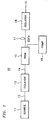
- Fig 1 illustrates in block form a portion of a typical optical network, 10, which can utilize the present invention.
- the light signal is generated by a source, 11, which is typically a laser such as an electroabsorption modulated laser (EML) which generates light having an exemplary wavelength of approx. 1550 nm.
- EML electroabsorption modulated laser
- the signal propogates through an optical fiber, 12, to an optical isolator, 13, which prevents reflection of the light signal back to the source, 11.
- the light signal continues to propogate through an optical fiber, 14, to a wavelength division multiplexer element (WDM), 15, which is designed to combine the signal light with light from a pump laser, 16.
- the WDM element is typically a high pass or low pass optical filter.
- the pump laser typically generates light with a wavelength of 980 nm or 1480 nm.
- the combined signal and pump light is coupled to a fiber amplifier, 17, such as an erbium doped fiber amplifier (EDFA), which amplifies the signal as a result of the pump light exciting the dopants in the fiber amplifier.
- EDFA erbium doped fiber amplifier
- the amplified signal light is coupled through a second isolator, 18, which, again, is designed to prevent backward reflection, and sent on to other portions of the network. While this example shows a pump laser, 16, coupled to propagate light through the amplifier, 17, in the same direction as the signal light, (co-propagating) the pump could be coupled so that the pump light propagates in a direction opposite to the signal light (counter-propagating).
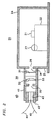
- Fig 2 illustrates an optical device package, 20, in accordance with an embodiment of the invention.
- An optical device, 21, such as a semiconductor pump laser, or another type of semiconductor laser, or a light emitting device, is exemplary mounted on a major surface of a substrate, 22, which is typically a silicon substrate.
- a substrate Preferably mounted within a groove in the surface of the substrate is a spherical lens, 23, for collimating the light emitted by the laser, 21.
- the substrate may also include many other elements, such as conductors, backface monitors and the like, which are not shown for purposes of simplicity. (For a more detailed discussion of an optical subassembly, see U.S. Patent No. 5,881,193 issued to Anigbo et al, which is incorporated by reference herein.)
- the substrate, 22, including the laser and lens is mounted within an enclosure, 24, which is typically made of an iron-nickel-cobalt alloy. While the substrate is shown mounted to the bottom of the enclosure in this example, it will be appreciated that it can be mounted to a pedestal or to the side walls of the enclosure.
- the enclosure, 24, includes a front wall, 25, with an aperture window, 26, formed therein.
- the laser, 21, and lens, 23, are aligned so that light from the laser is transmitted through the aperture, 26, when the laser is biased.
- An assembly, 30, preferably includes a WDM element, 31, another lens, 32, and a lens holder, 33, in which the WDM element and lens are mounted.
- the lens holder, 33 is a cylindrical tube made of a metal such as stainless steel so that the element, 31 and lens 32 may be epoxied to the inner wall of the tube.
- the tube includes openings, 34 and 35, on either end.
- the WDM element, 31, can be a typical multiplexing element made of a glass coated with a material which will transmit certain wavelengths and reflect certain other wavelengths as described in more detail below.
- the lens, 32 in this example, is an aspheric lens which is designed to focus light onto a fiber to be described.
- the assembly, 30, is mounted to the front wall, 25, of the enclosure, 24, so that the opening, 34, is aligned with the aperture window, 26, in the wall of the enclosure, 24. This can be done, for example, by welding the holder to the wall.
- An optical fiber termination, 40 is mounted to the end of the lens holder, 33, which includes the opening, 35, i.e. to the end of the tube which is remote from the enclosure, 24.
- the termination preferably includes a sleeve, 41, which is made of a metal such as stainless steel.
- the sleeve, 41 preferably has inserted therein a ferrule, 42, which is secured to the inner wall of the sleeve by laser welding.
- the ferrule is typically a metal such as stainless steel.
- a capillary, 43 which is usually made of ceramic and is secured to the ferrule by a press fit. Embedded within the capillary is at least one optical fiber.
- two fibers, 44 and 45 are embedded within the capillary by known techniques.
- the termination, 40 is mounted to the lens holder, 33 so that light from the input fiber, 44, is incident on the WDM element, 31, through the opening, 35, and the output fiber, 45, can receive light from the laser, 21, as well as reflected light from the WDM element, 31.
- the light signal from source, 11, would propogate through fiber, 44, of the package.
- the WDM element, 31, is coated so as to reflect at least a major portion of the wavelength of the signal light (e.g., 1550 nm), and the assembly, 30, and termination, 40, are aligned so that the signal light is reflected back to the output fiber, 45.
- light from the laser, 21, has a wavelength (e.g., 980 or 1480 nm) which is substantially transmitted through the WDM element, 31, and is also incident on the output fiber, 45 due to the alignment of the laser, 21, assembly, 30, and the termination 40.
- the device, 20, integrates the WDM and pump components, 15 and 16 (Fig. 1), into a single package.
- the device package, 20, can be assembled by various techniques.
- One possibility is to send light through the input fiber, 44, and measure the reflection from the WDM element to the output fiber, 45.
- the termination could be welded to the lens holder, 33.
- the combination of termination, 40, and assembly, 30, could be aligned with the laser 21 while the laser is emitting light.
- the lens holder, 33 can be welded to the wall, 25, of the enclosure.
Landscapes
- Physics & Mathematics (AREA)
- Condensed Matter Physics & Semiconductors (AREA)
- General Physics & Mathematics (AREA)
- Electromagnetism (AREA)
- Optics & Photonics (AREA)
- Optical Couplings Of Light Guides (AREA)
- Semiconductor Lasers (AREA)
- Lasers (AREA)
Applications Claiming Priority (2)
| Application Number | Priority Date | Filing Date | Title |
|---|---|---|---|
| US493749 | 2000-01-28 | ||
| US09/493,749 US6513991B1 (en) | 2000-01-28 | 2000-01-28 | Semiconductor optical device package |
Publications (2)
| Publication Number | Publication Date |
|---|---|
| EP1130707A2 true EP1130707A2 (de) | 2001-09-05 |
| EP1130707A3 EP1130707A3 (de) | 2003-05-28 |
Family
ID=23961541
Family Applications (1)
| Application Number | Title | Priority Date | Filing Date |
|---|---|---|---|
| EP01300636A Withdrawn EP1130707A3 (de) | 2000-01-28 | 2001-01-24 | Gehäuse für optische Halbleitervorrichtung |
Country Status (5)
| Country | Link |
|---|---|
| US (1) | US6513991B1 (de) |
| EP (1) | EP1130707A3 (de) |
| JP (1) | JP2001255437A (de) |
| CN (1) | CN1317897A (de) |
| CA (1) | CA2331911A1 (de) |
Families Citing this family (11)
| Publication number | Priority date | Publication date | Assignee | Title |
|---|---|---|---|---|
| US6715936B2 (en) * | 2002-01-22 | 2004-04-06 | Megasense, Inc. | Photonic component package and method of packaging |
| TW200306439A (en) * | 2002-03-27 | 2003-11-16 | Matsushita Electric Industrial Co Ltd | Optical composite module, optical wavelength multiplexer, optical wavelength demutiplexer, and optical composite module manufacturing method |
| US7422377B2 (en) * | 2003-06-30 | 2008-09-09 | Finisar Corporation | Micro-module with micro-lens |
| US7286736B2 (en) * | 2004-07-22 | 2007-10-23 | Finisar Corporation | Z-axis alignment of an optoelectronic component using a composite adhesive |
| JP2013507665A (ja) * | 2009-10-12 | 2013-03-04 | オクラロ テクノロジー リミテッド | 共同パッケージ化された半導体光学装置 |
| CN104238021B (zh) * | 2013-06-17 | 2017-12-01 | 上海中科股份有限公司 | 改善光无源器件耦合性能的方法 |
| CN105098577A (zh) * | 2015-09-02 | 2015-11-25 | 西安精英光电技术有限公司 | 一种基于球透镜耦合的尾纤激光器 |
| CN107402423A (zh) * | 2016-05-18 | 2017-11-28 | 刘向宁 | 一种光转换器 |
| WO2021223148A1 (en) * | 2020-05-07 | 2021-11-11 | Lumentum Operations Llc | Optical isolator core in between fiber and collimator lens |
| CN120150893A (zh) | 2020-05-07 | 2025-06-13 | 朗美通经营有限责任公司 | 光学隔离器芯 |
| CN114594555A (zh) * | 2020-12-03 | 2022-06-07 | 青岛海信宽带多媒体技术有限公司 | 一种光模块 |
Family Cites Families (14)
| Publication number | Priority date | Publication date | Assignee | Title |
|---|---|---|---|---|
| US4456329A (en) * | 1979-10-12 | 1984-06-26 | Westinghouse Electric Corp. | Optical device having multiple wavelength dependent optical paths |
| US4767171A (en) * | 1986-03-27 | 1988-08-30 | Siemens Aktiengesellschaft | Transmission and reception module for a bidirectional communication network |
| JPH01292875A (ja) * | 1988-05-20 | 1989-11-27 | Oki Electric Ind Co Ltd | 半導体光増幅モジュール |
| JPH02124504A (ja) * | 1988-11-02 | 1990-05-11 | Toshiba Corp | 受光モジュール |
| IT1227614B (it) * | 1988-12-22 | 1991-04-22 | Italtel Spa | Modulo ibrido ricetrasmittente per la trasmissione bidirezionale su una fibra ottica monomodale di due segnali ottici |
| US5452124A (en) * | 1994-03-04 | 1995-09-19 | Williams Telecommunications Group, Inc. | Unidirectional amplification for bi-directional transmission using wavelength-division multiplexing |
| JPH07261053A (ja) * | 1994-03-18 | 1995-10-13 | Fujitsu Ltd | 光合分波モジュール |
| US5555330A (en) * | 1994-12-21 | 1996-09-10 | E-Tek Dynamics, Inc. | Wavelength division multiplexed coupler with low crosstalk between channels and integrated coupler/isolator device |
| WO1996019743A1 (en) | 1994-12-21 | 1996-06-27 | E-Tek Dynamics, Inc. | Integrable fiberoptic coupler and resulting devices and systems |
| US5661835A (en) * | 1995-01-19 | 1997-08-26 | Sumitomo Electric Industries, Ltd. | Optical composite module and method of assembling the same |
| EP0782224B1 (de) | 1995-12-22 | 2000-12-20 | Lucent Technologies Inc. | Optische Unteranordnung mit niedriger Abmessung |
| JP3120828B2 (ja) * | 1996-04-08 | 2000-12-25 | 住友電気工業株式会社 | 半導体レーザモジュール |
| JPH10223962A (ja) * | 1997-02-12 | 1998-08-21 | Furukawa Electric Co Ltd:The | 光ファイバアンプ用複合モジュール |
| EP0939465A3 (de) * | 1998-02-26 | 2001-03-28 | Nec Corporation | Lichtquelle mit WDM-Funktion, optischer Verstärker und bidirektionales Ubertragungssystem unter Verwndung derselben |
-
2000
- 2000-01-28 US US09/493,749 patent/US6513991B1/en not_active Expired - Lifetime
-
2001
- 2001-01-23 CA CA002331911A patent/CA2331911A1/en not_active Abandoned
- 2001-01-23 CN CN01112333A patent/CN1317897A/zh active Pending
- 2001-01-24 EP EP01300636A patent/EP1130707A3/de not_active Withdrawn
- 2001-01-26 JP JP2001018524A patent/JP2001255437A/ja active Pending
Also Published As
| Publication number | Publication date |
|---|---|
| CN1317897A (zh) | 2001-10-17 |
| CA2331911A1 (en) | 2001-07-28 |
| JP2001255437A (ja) | 2001-09-21 |
| US6513991B1 (en) | 2003-02-04 |
| EP1130707A3 (de) | 2003-05-28 |
Similar Documents
| Publication | Publication Date | Title |
|---|---|---|
| EP0343489B1 (de) | Optischer Verstärkungsmodul | |
| JP2786725B2 (ja) | 光ファイバおよびファイバ光能動装置 | |
| US5170458A (en) | Optical fiber light-amplifier system | |
| EP0812039A2 (de) | Faserlichtquelle mit Multimodefaserkoppler | |
| US20030206335A1 (en) | Erbium-doped fiber amplifier and integrated module components | |
| EP1033795A2 (de) | Optische Faser mit doppelten Mantel und Faseroptischer Verstärker | |
| US6513991B1 (en) | Semiconductor optical device package | |
| US6310717B1 (en) | Optical amplifier and fiber module for optical amplification | |
| EP1128502A2 (de) | Optischer Verstärker mit massiver Optik ("bulk") | |
| CN1373920A (zh) | 集成了光学通道波导放大器和抽运源的紧凑型光学放大器组件 | |
| US6330117B1 (en) | Optical isolator module and optical amplifier using the same | |
| US20030215241A1 (en) | Raman optical fiber amplifier using erbium doped fiber | |
| JPH05343785A (ja) | 光増幅器用光モジュール | |
| US6532107B2 (en) | Optical amplifier, light source module and optical system | |
| WO2001016637A1 (en) | Integrated wavelength selective photodiode module | |
| JP2003188444A (ja) | 光増幅器 | |
| JPH0888430A (ja) | 光ファイバ増幅器 | |
| WO1997039460A1 (en) | Lasers diode pump with optical fiber filter | |
| JP2005345694A (ja) | 光集積化モジュール | |
| JPH07294329A (ja) | 光パワーモニタ装置、およびこれを用いた光増幅装置 | |
| JP2000105325A (ja) | 光ファイバーコリメータとこれを用いた光モジュール及び光増幅器 | |
| JP3042439B2 (ja) | 光ファイバ増幅器 | |
| JPH07335956A (ja) | 光増幅器及び受光装置 | |
| JP3833280B2 (ja) | 光学部品 | |
| JPH04253037A (ja) | マルチファイバ光増幅器およびそれを用いた多心光フ ァイバの接続構造 |
Legal Events
| Date | Code | Title | Description |
|---|---|---|---|
| PUAI | Public reference made under article 153(3) epc to a published international application that has entered the european phase |
Free format text: ORIGINAL CODE: 0009012 |
|
| AK | Designated contracting states |
Kind code of ref document: A2 Designated state(s): AT BE CH CY DE DK ES FI FR GB GR IE IT LI LU MC NL PT SE TR |
|
| AX | Request for extension of the european patent |
Free format text: AL;LT;LV;MK;RO;SI |
|
| RAP1 | Party data changed (applicant data changed or rights of an application transferred) |
Owner name: AGERE SYSTEMS OPTOELECTRONICS GUARDIAN CORPORATION |
|
| PUAL | Search report despatched |
Free format text: ORIGINAL CODE: 0009013 |
|
| AK | Designated contracting states |
Designated state(s): AT BE CH CY DE DK ES FI FR GB GR IE IT LI LU MC NL PT SE TR |
|
| AX | Request for extension of the european patent |
Extension state: AL LT LV MK RO SI |
|
| 17P | Request for examination filed |
Effective date: 20031021 |
|
| AKX | Designation fees paid |
Designated state(s): DE FR GB |
|
| 17Q | First examination report despatched |
Effective date: 20040128 |
|
| STAA | Information on the status of an ep patent application or granted ep patent |
Free format text: STATUS: THE APPLICATION IS DEEMED TO BE WITHDRAWN |
|
| 18D | Application deemed to be withdrawn |
Effective date: 20041125 |