EP1128490A2 - EMV-Kontaktierung zwischen einem metallisch geschirmten Steckergehäuse und einem Steckerdurchbruch sowie Stanzstempel und Verfahren zur Herstellung eines Steckerdurchbruches - Google Patents
EMV-Kontaktierung zwischen einem metallisch geschirmten Steckergehäuse und einem Steckerdurchbruch sowie Stanzstempel und Verfahren zur Herstellung eines Steckerdurchbruches Download PDFInfo
- Publication number
- EP1128490A2 EP1128490A2 EP01104167A EP01104167A EP1128490A2 EP 1128490 A2 EP1128490 A2 EP 1128490A2 EP 01104167 A EP01104167 A EP 01104167A EP 01104167 A EP01104167 A EP 01104167A EP 1128490 A2 EP1128490 A2 EP 1128490A2
- Authority
- EP
- European Patent Office
- Prior art keywords
- tips
- metallic wall
- plug opening
- plug
- punching
- Prior art date
- Legal status (The legal status is an assumption and is not a legal conclusion. Google has not performed a legal analysis and makes no representation as to the accuracy of the status listed.)
- Withdrawn
Links
- 238000004519 manufacturing process Methods 0.000 title claims abstract description 13
- 239000002184 metal Substances 0.000 title claims description 5
- 238000004080 punching Methods 0.000 claims description 25
- 238000000034 method Methods 0.000 claims description 15
- 238000003780 insertion Methods 0.000 claims description 4
- 230000037431 insertion Effects 0.000 claims description 4
- 208000008918 voyeurism Diseases 0.000 description 4
- 239000000463 material Substances 0.000 description 3
- 230000015556 catabolic process Effects 0.000 description 1
- 210000003746 feather Anatomy 0.000 description 1
- 238000007373 indentation Methods 0.000 description 1
- 230000013011 mating Effects 0.000 description 1
- 230000035515 penetration Effects 0.000 description 1
Images



Classifications
-
- H—ELECTRICITY
- H01—ELECTRIC ELEMENTS
- H01R—ELECTRICALLY-CONDUCTIVE CONNECTIONS; STRUCTURAL ASSOCIATIONS OF A PLURALITY OF MUTUALLY-INSULATED ELECTRICAL CONNECTING ELEMENTS; COUPLING DEVICES; CURRENT COLLECTORS
- H01R13/00—Details of coupling devices of the kinds covered by groups H01R12/70 or H01R24/00 - H01R33/00
- H01R13/73—Means for mounting coupling parts to apparatus or structures, e.g. to a wall
- H01R13/74—Means for mounting coupling parts in openings of a panel
-
- H—ELECTRICITY
- H01—ELECTRIC ELEMENTS
- H01R—ELECTRICALLY-CONDUCTIVE CONNECTIONS; STRUCTURAL ASSOCIATIONS OF A PLURALITY OF MUTUALLY-INSULATED ELECTRICAL CONNECTING ELEMENTS; COUPLING DEVICES; CURRENT COLLECTORS
- H01R13/00—Details of coupling devices of the kinds covered by groups H01R12/70 or H01R24/00 - H01R33/00
- H01R13/648—Protective earth or shield arrangements on coupling devices, e.g. anti-static shielding
- H01R13/658—High frequency shielding arrangements, e.g. against EMI [Electro-Magnetic Interference] or EMP [Electro-Magnetic Pulse]
- H01R13/6591—Specific features or arrangements of connection of shield to conductive members
- H01R13/6596—Specific features or arrangements of connection of shield to conductive members the conductive member being a metal grounding panel
-
- H—ELECTRICITY
- H01—ELECTRIC ELEMENTS
- H01R—ELECTRICALLY-CONDUCTIVE CONNECTIONS; STRUCTURAL ASSOCIATIONS OF A PLURALITY OF MUTUALLY-INSULATED ELECTRICAL CONNECTING ELEMENTS; COUPLING DEVICES; CURRENT COLLECTORS
- H01R4/00—Electrically-conductive connections between two or more conductive members in direct contact, i.e. touching one another; Means for effecting or maintaining such contact; Electrically-conductive connections having two or more spaced connecting locations for conductors and using contact members penetrating insulation
- H01R4/26—Connections in which at least one of the connecting parts has projections which bite into or engage the other connecting part in order to improve the contact
Definitions
- the invention relates on the one hand to the EMC contact between a metallic shielded connector housing and one Plug breakthrough in a metallic wall, such as the panel on a PC module card.
- the invention further relates to a punch for producing a such connector breakdown as well as the procedure for Making the connector opening.
- the invention is therefore based on the object of being reliable EMC contact between a metallic connector housing and to show a plug breakthrough which the cost and assembly effort is reduced, and also the tool and the method for solving this task specify.
- the object is achieved according to the invention solved in that peaks at the connector opening are formed in when plugging in the connector housing penetrate the connector opening into the connector housing and contact this.
- the tips can be in the plane and / or perpendicular to be metallic wall. Are the tips vertical formed to the metallic wall, the connector housing a collar in which the tips when inserted penetration.
- the task is done by a stamp solved, which essentially the outer geometry of the connector opening has and laterally starting from the punching surface provided with depressions running in the punching direction through which the peaks are formed.
- the task is alternatively solved in that a stamp with roundings on the edge of the punching surface is used is, the area of the plug opening is a multiple the punching area and the stamp with each punching process is so much laterally offset that the rounding the tips remain at the edge of the connector opening.
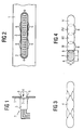
- Figure 1 shows a side view of a metallic wall 1 with a plug inserted therein 2.
- the plug 2 points a metal shielded connector housing 3, which so inserted into a connector opening 4 in the metallic wall is that there is contact between the connector housing 3 and the metallic wall 1 is formed.
- the shielding can consist of metal or metallized plastic.
- a circumferential collar 5 is formed.
- the metallic wall 1 is cut according to FIG shown.
- the metallic wall 1 can, for example, the Cover of a PC module card or the rear wall of a PC housing his.
- Figure 2 shows the representation of Figure 1 in the view from the front, i.e. with a view of the mating face of the connector 2.
- the circumferentially distributed tips 6 reach into that Plug housing 3 and thus ensure ideal EMC contacting.
- Figure 4 shows schematically how the plug opening 4 according to Figure 3 is made.
- a punch 7 is used for this, which has a much smaller punching area than that Plug opening 4 has.
- the punch 7 has the width b of the connector opening 4, but a much shorter length 1 than that Plug opening 4 on.
- the punch is 7 at the end provided with a rounding 8, which on the rounding is matched to the connector housing 3.
- the punch is made by one Punching process to the next offset so far that by the partially overlap the rounding 8 at the edge of the connector opening 4 a tip 6 remains on both sides.
- the manufacture of the connector breakthrough with tips in the Plane breakthrough level can also be single Punching process.
- Figure 5 shows a side view of what is required for this Stamp 9. This is on the side at the places where the tips 6 should remain, each with the corresponding Provide depressions 10.
- Figure 6 shows the section VI-VI of Figure 5.
- the punch 9 has essentially the cross section of the plug opening 4, the recesses 10 on both sides on the lower sides are provided.
- the depressions 10 are wedge-shaped, to leave sharp points.
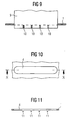
- the punching process is shown in FIG. 7, the punching stamp 9 is lowered so far that the punch 9 punched out the plug opening 4 of the metallic wall 1, however, the indentations 10 do not over the top of the metallic Wall 1 are lowered so that the tips 6 remain in the plane of the metallic wall.
- FIG 8 shows such an embodiment.
- metallic wall 1 are opposite the direction of insertion protruding perpendicular to the metallic wall 1 Tips 11 provided.
- the connector 2 is in the figure 8 shown state is not yet completely in the Plug opening 4 'inserted.
- On the connector housing 3 is also a circumferential protruding collar 5 is formed, in which the essentially perpendicular from the metallic Wall 1 protruding tips 11 when fully inserted Penetrate plug 2 and thus a reliable EMC contact between metallic wall 1 and plug 2 form.
- the manufacture of the tips 11 takes place in the Figures 5 to 7 described punch 9.
- Figure 11 shows the section X-X of Figure 10. In this Cut is easy to see, like the tips 11 down and project substantially perpendicular to the metallic wall 1.
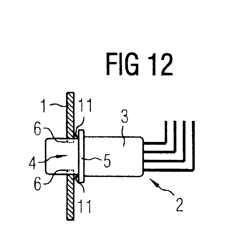
- Figure 12 shows a sectional representation of the metallic Wall 1 with tips 6 in the plane of the metallic wall 1 and tips 11 opposite to the insertion direction of the to be inserted Connector 2.
- the shown in side view metallic connector housing 3 also has in this embodiment a collar 5, which the tips 11 at Contact completely inserted plug. In the illustrated The plug 2 is not fully inserted.
- the punch 12 points to both lower sides recesses 10 and 10 ', the Wells 10 over the height h and wells 10 'over the greater height H are formed.
- FIG. 14 shows the section XIII-XIII from FIG. 13.
- the depressions 10 and 10 ' are on both sides and alternate arranged.
- the connector opening 4 '' punched out in a first step in this step still all peaks in the plane of the metallic wall 1 arranged are.
- the punch 12 lowered so far that the depressions 10 with the height h below the lower edge the metallic wall 1 and the recesses 10 ' with size H still in the area of the metallic wall 1 are arranged. All tips through the recesses 10 were thus formed at this step down bent and are thus essentially perpendicular to the metallic wall 1 from.
- FIG. 17 shows the resulting plug opening 4 '' the peaks arranged in the plane of the metallic wall 6 and FIG. 18 shows the section XVII-XVII from FIG. 17, in which both in the plane of the metallic wall 1 arranged tips 6 and the perpendicular from the metallic Wall 1 protruding tips 11 can be seen.
- tips for EMC contacting between metallic connector housing and metallic PC card cover or PC back wall becomes easy Manufactured and inexpensive shielding achieved because the Tips as described above are easy to manufacture and additional Avoid contact materials such as springs and gasket can be.
Landscapes
- Details Of Connecting Devices For Male And Female Coupling (AREA)
- Shielding Devices Or Components To Electric Or Magnetic Fields (AREA)
Abstract
Description
- Figur 1
- eine Schnittansicht einer ersten Ausführungsform der metallischen Wandung mit Spitzen in der Ebene der Wandung sowie dem eingesetzten Steckergehäuse in Seitenansicht,
- Figur 2
- eine frontale Ansicht des in die metallische Wandung eingesteckten Steckergehäuses,
- Figur 3
- die Umrißlinie eines Steckerdurchbruchs,
- Figur 4
- den Stanzvorgang zur Bildung des Steckerdurchbruchs nach Fig. 3 mit einem im Querschnitt dargestellten Stanzstempel,
- Figur 5
- eine Seitenansicht einer zweiten Variante eines Stanzstempels,
- Figur 6
- den Schnitt VI-VI aus Figur 5,
- Figur 7
- den Stanzstempel gemäß Figur 5 im Stanzvorgang,
- Figur 8
- die Schnittansicht einer zweiten Ausführungsform der metallischen Wandung mit Spitzen entgegen der Steckrichtung sowie dem eingesetzten Steckergehäuse in Seitenansicht,
- Figur 9
- eine Seitenansicht des Stanzstempels im Tiefziehschritt zur Ausbildung der Spitzen gemäß Figur 8,
- Figur 10
- die Umrißlinie des Stanzgratsdurchbruchs nach dem Stanzvorgang gemäß Figur 9,
- Figur 11
- den Schnitt X-X gemäß Figur 10,
- Figur 12
- die Schnittansicht einer dritten Ausführungsform der metallischen Wandung mit Spitzen in Richtung Steckerdurchbruch sowie senkrecht zum Steckerdurchbruch sowie dem eingesetzten Steckergehäuse in Seitenansicht,
- Figur 13
- den Stanzstempel in der Ausführung gemäß Figur 12,
- Figur 14
- den Schnitt XIII-XIII aus Figur 13,
- Figur 15
- eine Seitenansicht des Stanzvorganges im ersten Schritt,
- Figur 16
- eine Seitenansicht des Stanzvorganges im zweiten Schritt,
- Figur 17
- der resultierende Steckerdurchbruch in der Draufsicht und
- Figur 18
- den Schnitt XVII-XVII aus Figur 17.
Claims (9)
- EMV-Kontaktierung zwischen einem metallisch geschirmten Steckergehäuse (3) und einem Steckerdurchbruch (4, 4', 4'') in einer metallischen Wandung (1), wie zum Beispiel der Blende einer PC-Baugruppenkarte,
dadurch gekennzeichnet, daß
an dem Steckerdurchbruch (4, 4', 4'') Spitzen (6, 11) ausgebildet sind, die beim Einstecken des Steckergehäuses (3) in den Steckerdurchbruch in das Steckergehäuse (3) eindringen und dieses somit kontaktieren. - EMV-Kontaktierung nach Anspruch 1,
dadurch gekennzeichnet, daß
die Spitzen (6) in der Ebene der metallischen Wandung (1) angeordnet sind und in Richtung Steckerdurchbruch (4) zeigen. - EMV-Kontaktierung nach Anspruch 1,
dadurch gekennzeichnet, daß
die Spitzen (11) entgegengesetzt zur Steckrichtung angeordnet sind und einen am Steckergehäuse (3) angeordneten Kragen (5) kontaktieren. - Verfahren zum Herstellen eines Steckerdurchbruches (4) in einer metallischen Wandung (1) mit Spitzen (6) in der Ebene der metallischen Wandung (1),
dadurch gekennzeichnet, daß der Stekkerdurchbruch (4) mit den Spitzen (6) durch Stanzen erzeugt wird und ein Stempel (7) mit Abrundungen (8) verwendet wird, wobei die Fläche des Steckerdurchbruches (4) ein Vielfaches der Fläche des Stempels (7) beträgt und der Stempel (7) nach jedem Stanzvorgang so seitlich versetzt wird, daß durch die Abrundungen (8) am Rand des Steckerdurchbruches (4) Spitzen (6) verbleiben. - Stanzstempel (9, 12) zur Herstellung eines Steckerdurchbruches (4, 4', 4'') mit Spitzen (6, 11),
gekennzeichnet dadurch, daß
er im wesentlichen die Außengeometrie des Steckerdurchbruches (4, 4', 4'') aufweist und seitlich abgehend von der Stanzfläche mit in Stanzrichtung verlaufenden Vertiefungen (10, 10') versehen ist, durch welche die Spitzen (6, 11) gebildet werden. - Stanzstempel nach Anspruch 5,
dadurch gekennzeichnet, daß
zwei Arten von Vertiefungen (10, 10') vorgesehen sind, wobei die ersteren Vertiefungen (10) in Stanzrichtung eine Höhe (h) und die zweite Art von Vertiefungen (10') eine Höhe (H) aufweisen und die Höhe (H) größer als (h) ist. - Verfahren zur Herstellung eines Steckerdurchbruches (4) in einer metallischen Wandung (1) mit Spitzen (6) in der Ebene der metallischen Wandung,
gekennzeichnet dadurch, daß
der Steckerdurchbruch (4) mit den Spitzen (6) durch Stanzen erzeugt wird und ein Stanzstempel (9) nach Anspruch 5 verwendet wird und der Stanzweg nicht die Höhe der Vertiefungen (10) übersteigt. - Verfahren zur Herstellung eines Steckerdurchbruches (4') in einer metallischen Wandung (1) mit Spitzen (11), die im wesentlichen senkrecht zur Ebene der metallischen Wandung (1) angeordnet sind,
dadurch gekennzeichnet, daß
der Steckerdurchbruch (4') mit den Spitzen (6) durch Stanzen erzeugt wird und ein Stempel (9) nach Anspruch 5 verwendet wird und der Stanzweg die Höhe der Vertiefungen (10) übersteigt. - Verfahren zur Herstellung eines Steckerdurchbruches (4'') in einer metallischen Wandung (1) mit Spitzen (6, 11) in der Ebene und senkrecht zur Ebene der metallischen Wandung,
dadurch gekennzeichnet, daß
der Steckerdurchbruch (4'') mit den Spitzen (6, 11) durch Stanzen erzeugt wird und ein Stempel (12) nach Anspruch 6 verwendet wird und der Stanzweg die Höhe (h) der ersten Art von Vertiefungen (10) übersteigt, jedoch die zweite Art von Vertiefungen (10') mit der Höhe (H) noch in der Ebene der metallischen Wandung (1) angeordnet sind.
Applications Claiming Priority (2)
| Application Number | Priority Date | Filing Date | Title |
|---|---|---|---|
| DE10008281 | 2000-02-23 | ||
| DE2000108281 DE10008281C2 (de) | 2000-02-23 | 2000-02-23 | EMV-Kontaktierung zwischen einem metallisch geschirmten Steckergehäuse und einem Steckerdurchbruch sowie Stanzstempel und Verfahren zur Herstellung eines Steckerdurchbruches |
Publications (2)
| Publication Number | Publication Date |
|---|---|
| EP1128490A2 true EP1128490A2 (de) | 2001-08-29 |
| EP1128490A3 EP1128490A3 (de) | 2001-11-14 |
Family
ID=7631993
Family Applications (1)
| Application Number | Title | Priority Date | Filing Date |
|---|---|---|---|
| EP01104167A Withdrawn EP1128490A3 (de) | 2000-02-23 | 2001-02-21 | EMV-Kontaktierung zwischen einem metallisch geschirmten Steckergehäuse und einem Steckerdurchbruch sowie Stanzstempel und Verfahren zur Herstellung eines Steckerdurchbruches |
Country Status (2)
| Country | Link |
|---|---|
| EP (1) | EP1128490A3 (de) |
| DE (1) | DE10008281C2 (de) |
Families Citing this family (1)
| Publication number | Priority date | Publication date | Assignee | Title |
|---|---|---|---|---|
| DE102006024736B4 (de) * | 2006-05-26 | 2013-05-23 | Siemens Aktiengesellschaft | Kontaktvorrichtung |
Family Cites Families (9)
| Publication number | Priority date | Publication date | Assignee | Title |
|---|---|---|---|---|
| FR2420223A1 (fr) * | 1978-03-14 | 1979-10-12 | Oeillets Metalliques Manuf Fse | Ensemble de contact electrique |
| DE8902245U1 (de) * | 1989-02-25 | 1989-05-11 | Thomas & Betts Corp., Bridgewater, N.J. | Vielfachstecker |
| FR2652228B1 (fr) * | 1989-09-19 | 1996-05-24 | Bull Sa | Chassis de blindage pour la protection, contre les effets de rayonnements electromagnetiques, d'un circuit electrique place a l'interieur de ce chassis. |
| DE8911765U1 (de) * | 1989-10-03 | 1991-01-31 | Ramsauer, Dieter, 5620 Velbert | Verschlußgehäuse mit Flansch zur Montage in einem Durchbruch einer dünnwandigen Fläche, insbesondere Blechschranktür oder Blechkastendeckel |
| FR2679706B1 (fr) * | 1991-07-24 | 1995-05-12 | Cit Alcatel | Dispositif de protection d'un element de connecteur multibroches contre les perturbations electromagnetiques. |
| SE502705C2 (sv) * | 1994-04-07 | 1995-12-11 | Ellemtel Utvecklings Ab | Anordning för att EMC-skärma en in- eller utgående kabel eller liknande |
| SE502998C2 (sv) * | 1994-06-10 | 1996-03-11 | Ericsson Telefon Ab L M | Elektriskt kopplingsdon samt kretskort |
| EP0887894B1 (de) * | 1997-06-27 | 2004-08-04 | International Business Machines Corporation | Sicherungsplatte für Leiterplattenkabelverbinder |
| DE19745112A1 (de) * | 1997-10-11 | 1999-04-15 | Abb Daimler Benz Transp | Isolierbuchsensystem für die Befestigung eines elektrischen Leistungsanschlusses |
-
2000
- 2000-02-23 DE DE2000108281 patent/DE10008281C2/de not_active Expired - Fee Related
-
2001
- 2001-02-21 EP EP01104167A patent/EP1128490A3/de not_active Withdrawn
Also Published As
| Publication number | Publication date |
|---|---|
| DE10008281C2 (de) | 2002-04-18 |
| DE10008281A1 (de) | 2001-09-27 |
| EP1128490A3 (de) | 2001-11-14 |
Similar Documents
| Publication | Publication Date | Title |
|---|---|---|
| DE68917080T2 (de) | Elektrischer Verbinder für elektronische Gedächtniskarten, Verfahren der Verwirklichung eines derartigen Verbinders und Lese-Schreibvorrichtung mit diesem Verbinder. | |
| DE10321348B4 (de) | Steckverbinder | |
| EP0059462B1 (de) | Einpressstift | |
| DE4018164C2 (de) | Schneidklemm-Kontakt | |
| DE2312749A1 (de) | Loetbuchse fuer gedruckte schaltungen | |
| DE102006011657A1 (de) | Kontaktstift und Verfahren zu dessen Herstellung | |
| DE102015211002B4 (de) | Verbinder mit einem Verbindergehäuse und einem Verbinderanschluss | |
| DE1540154B2 (de) | In dem loch einer platte aus hartem, sproedem und nur schwach elastischem werkstoff befestigter elektrischer anschlusstift | |
| DE68923016T2 (de) | Elektrischer Endstückstift mit nachgiebigem Teil. | |
| EP3637556B1 (de) | Abgewinkleter steckverbinder mit abschirmung | |
| WO2008025611A1 (de) | Einpressstift | |
| EP0198408B1 (de) | Werkzeug zur Herstellung eines elektrischen Kontaktstiftes für gedruckte Schaltungsplatten | |
| DE2907417C2 (de) | ||
| EP0662733A2 (de) | Kontaktfeder-Anordnung | |
| DE102007035325A1 (de) | Stiftförmiges Kontaktelement und Steckverbindung | |
| DE3324737C2 (de) | ||
| EP1885029A1 (de) | Elektrisches Anschlusselement | |
| EP0833406A2 (de) | Einpressstift mit einem elastischen Einpressbereich | |
| EP0952765B1 (de) | Kontaktstreifen zum elektrischen Kontaktieren und/oder zur Erzielung einer gegen hochfrequente elektromagnetische Wellen dichten Verbindung sowie zugehörige Abschirmanordnung | |
| DE10008281C2 (de) | EMV-Kontaktierung zwischen einem metallisch geschirmten Steckergehäuse und einem Steckerdurchbruch sowie Stanzstempel und Verfahren zur Herstellung eines Steckerdurchbruches | |
| DE2336244B2 (de) | Anklemmbares Kontaktplättchen für flache elektrische Schaltkreise | |
| DE19833248C2 (de) | Vorrichtung zum Führen und Massekontaktieren von Leiterplatten | |
| DE19616786C2 (de) | Kontaktschalter | |
| DE102010040561A1 (de) | Verfahren zum Herstellen von stiftförmigen Kontaktelementen und Kontaktelement | |
| EP1469568B1 (de) | Steckkontaktelement und Verfahren zur Herstellung eines Gehäuseteils für dieses |
Legal Events
| Date | Code | Title | Description |
|---|---|---|---|
| PUAI | Public reference made under article 153(3) epc to a published international application that has entered the european phase |
Free format text: ORIGINAL CODE: 0009012 |
|
| AK | Designated contracting states |
Kind code of ref document: A2 Designated state(s): AT BE CH CY DE DK ES FI FR GB GR IE IT LI LU MC NL PT SE TR |
|
| AX | Request for extension of the european patent |
Free format text: AL;LT;LV;MK;RO;SI |
|
| PUAL | Search report despatched |
Free format text: ORIGINAL CODE: 0009013 |
|
| AK | Designated contracting states |
Kind code of ref document: A3 Designated state(s): AT BE CH CY DE DK ES FI FR GB GR IE IT LI LU MC NL PT SE TR |
|
| AX | Request for extension of the european patent |
Free format text: AL;LT;LV;MK;RO;SI |
|
| 17P | Request for examination filed |
Effective date: 20020508 |
|
| AKX | Designation fees paid |
Free format text: AT BE CH CY DE DK ES FI FR GB GR IE IT LI LU MC NL PT SE TR |
|
| 17Q | First examination report despatched |
Effective date: 20020722 |
|
| STAA | Information on the status of an ep patent application or granted ep patent |
Free format text: STATUS: THE APPLICATION IS DEEMED TO BE WITHDRAWN |
|
| 18D | Application deemed to be withdrawn |
Effective date: 20030204 |