EP1126652A2 - Procédé et système de transmission et réception de signaux multiplexés de façon asynchrone - Google Patents
Procédé et système de transmission et réception de signaux multiplexés de façon asynchrone Download PDFInfo
- Publication number
- EP1126652A2 EP1126652A2 EP01102886A EP01102886A EP1126652A2 EP 1126652 A2 EP1126652 A2 EP 1126652A2 EP 01102886 A EP01102886 A EP 01102886A EP 01102886 A EP01102886 A EP 01102886A EP 1126652 A2 EP1126652 A2 EP 1126652A2
- Authority
- EP
- European Patent Office
- Prior art keywords
- data unit
- error check
- header bits
- error
- header
- Prior art date
- Legal status (The legal status is an assumption and is not a legal conclusion. Google has not performed a legal analysis and makes no representation as to the accuracy of the status listed.)
- Withdrawn
Links
Images


Classifications
-
- H—ELECTRICITY
- H04—ELECTRIC COMMUNICATION TECHNIQUE
- H04L—TRANSMISSION OF DIGITAL INFORMATION, e.g. TELEGRAPHIC COMMUNICATION
- H04L1/00—Arrangements for detecting or preventing errors in the information received
- H04L1/004—Arrangements for detecting or preventing errors in the information received by using forward error control
- H04L1/0056—Systems characterized by the type of code used
- H04L1/0061—Error detection codes
-
- H—ELECTRICITY
- H04—ELECTRIC COMMUNICATION TECHNIQUE
- H04L—TRANSMISSION OF DIGITAL INFORMATION, e.g. TELEGRAPHIC COMMUNICATION
- H04L1/00—Arrangements for detecting or preventing errors in the information received
- H04L1/004—Arrangements for detecting or preventing errors in the information received by using forward error control
- H04L1/0072—Error control for data other than payload data, e.g. control data
-
- H—ELECTRICITY
- H04—ELECTRIC COMMUNICATION TECHNIQUE
- H04L—TRANSMISSION OF DIGITAL INFORMATION, e.g. TELEGRAPHIC COMMUNICATION
- H04L1/00—Arrangements for detecting or preventing errors in the information received
- H04L1/0078—Avoidance of errors by organising the transmitted data in a format specifically designed to deal with errors, e.g. location
- H04L1/0079—Formats for control data
-
- H—ELECTRICITY
- H04—ELECTRIC COMMUNICATION TECHNIQUE
- H04L—TRANSMISSION OF DIGITAL INFORMATION, e.g. TELEGRAPHIC COMMUNICATION
- H04L1/00—Arrangements for detecting or preventing errors in the information received
- H04L1/0078—Avoidance of errors by organising the transmitted data in a format specifically designed to deal with errors, e.g. location
- H04L1/0085—Formatting with cells
Definitions
- the present invention relates generally to communications systems and more specifically to a method and system for transmission and reception of asynchronously (statistically) multiplexed signals onto a common transmission medium.
- the present invention is particularly useful for asynchronously multiplexing data units of different format such as ATM cells and frames (i.e., layer-2 frames) in which IP (Internet Protocol) packets are encapsulated.
- the object of the present invention is obtained by forming data units so that the header of each of the data units contains an equal number of physical header bits and an header error check code resulting from division of the physical header bits by an identical generator polynomial and then summing to the header error check code a remainder of division of hypothetical header bits by the generator polynomial, the hypothetical header bits being greater in number than the physical header bits.
- a communication method comprising the steps of receiving a first data unit containing first header bits of a first payload signal and a first error check code representing a remainder of division of the first header bits by a generator polynomial, the first header bits being equal in number to second header bits of a second payload signal of a second data unit, the generator polynomial being used to divide the second header bits to produce a second error check code, and summing a remainder of division of hypothetical header bits by the generator polynomial to the first error check code, the hypothetical header bits being greater in number than the first header bits, whereby the first and second data units can be distinguished from each other by different error check results of the first and second data units.
- the hypothetical header bits are composed of higher significant bits of non-zero value and all-zero lower significant bits, the lower significant bits being equal in number to the first header bits plus the error check code. Further, the hypothetical header bits may correspond in number to the maximum degree of an irreducible polynomial.
- the first and second data units are asynchronously multiplexed onto a common medium and transmitted to a receive site.
- an error check is performed on the header bits of the multiplexed signal by using the same generator polynomial as that used in the transmit site to produce a first result.
- a second result is produced by summing to the first result the same second remainder as that produced at the transmit site.
- a decision is made as to whether the received signal corresponds to the first data unit or the second data unit.
- the receive site identifies the received signal as a first data unit when it detects the presence of a one-bit error in the first result and no bit error in the second result and identifies the received signal as a second data unit when it detects the presence of a one-bit error in the second result and no bit error in the first result. Further, the receive site identifies the received signal as a first data unit when it detects the presence of a two-bit error in the first result and a one-bit error in the second result and identifies the received signal as a second data unit when it detects the presence of a two-bit error in the second result and a one-bit error in the first result.
- the first data unit is a layer-2 frame in which layer-3 packets are encapsulated and the second data unit is an ATM cell.
- the generator polynomial is x 8 + x 2 + x + 1 which is used to divide the hypothetical header bits which may extend up to 127 bits.
- the hypothetical header bits are composed of all-zero lower-significant bits which are in the range from the 0-th to the 39-th bit position corresponding to the first header bits, and higher-significant bits of non-zero value which are in the range from the 40-th to the 126-th bit position.
- an error check is performed on the header bits of a multiplexed data unit by using the generator polynomial x 8 + x 2 + x + 1 to produce a result.
- a sum of the constant value and the second remainder as those used at the transmit site is added to the result to produce a first added result, and the same second remainder is added to the result to produce a second added result.
- a decision is made as to whether the received signal is a layer-2 frame or an ATM cell.
- the amount of information carried by the multiplexed first data unit may be limited when the second data unit is requesting high quality of service and an idle data unit may be transmitted when the first and second data units are not present on the common medium.
- the second data units may be transmitted immediately following the start timing of a superframe and the first data units follow when the second data units are requesting high quality of service.
- the present invention provides a communication method comprising the steps of producing, for a first payload signal of a first data unit, first header bits equal in number to second header bits of a second payload signal of a second data unit, dividing the first header bits by a generator polynomial to produce a first error check code, the generator polynomial being equal to a generator polynomial with which the second header bits are divided to produce a second error check code, producing a sum of a remainder of division of hypothetical header bits by the generator polynomial to the first error check code, the hypothetical header bits being greater in number than the second header bits, and forming the first data unit with the second header bits, the sum and the first payload signal, whereby the first and second data units can be distinguished from each other by different error check results of the first and second data units.
- the present invention provides a communication method which comprises transmitting a first data unit containing first header bits, a first error check code and a first payload signal through a transmission medium, and receiving the first data unit through the transmission medium and producing a sum of a remainder of division of hypothetical header bits by that generator polynomial to the first error check code, the hypothetical header bits being greater in number than the first header bits, and reformulating a first data unit with the first header bits, the sum and the first payload signal, whereby the reformulated first data unit can be distinguished from a second data unit by different error check results of the first and second data units, wherein the second data unit contains second headers equal in number to the first header bits, a second error check code resulting from division of the second header bits by that generator polynomial.
- a first data unit is transmitted from a transmit site through a transmission medium, the first data unit containing header bits and a sum of a first error check code resulting from division of the first header bits with a generator polynomial and a remainder resulting from division by that generator polynomial of hypothetical header bits greater in number than the first header bits.
- the first data unit is received by a receive site, where that remainder is subtracted from the received first data unit, whereby the received first data unit is converted to a data unit which can be distinguished from a data unit which is identical in format to the received first data unit.
- the present invention provides a communication circuit comprising a storage circuit including a first field for storing first header bits of a first payload signal of a first data unit, a second field containing a first error check code resulting from division of the first header bits by a generator polynomial, and a third field for storing the first payload signal, the first header bits being equal in number to second header bits of a second payload signal of a second data unit, and the generator polynomial being used to divide the second header bits to produce a second error check code, and an adder circuit for summing a remainder of division of hypothetical header bits by the generator polynomial to the first error check code, the hypothetical header bits being greater in number than a total number of bits in the first and second fields, whereby the first data unit can be distinguished from each other by different error check results of the first and second data units.
- the present invention provides a communication circuit comprising a storage circuit including a first field for storing first header bits of a first payload signal of a first data unit, a second field, and a third field for storing the first payload signal, the first header bits being equal in number to second header bits of a second payload signal of a second data unit, and the generator polynomial being used to divide the second header bits to produce a second error check code, division circuitry for dividing the first header bits by the generator polynomial to produce a first error check code, and an adder for summing a remainder of division of hypothetical header bits by the generator polynomial to the first error check code to produce a sum and inserting the sum into the second field of the storage circuit, the hypothetical header bits being greater in number than a total number of bits in the first and second fields, whereby the first and second data units can be distinguished from each other by different error check results of the first and second data units.
- the present invention provides a communication circuit comprising a storage circuit including a first field for storing first header bits of a first payload signal of a received first data unit, a second field containing a first error check code which equals a sum of a first remainder resulting from division of the first header bits by a generator polynomial and a second remainder resulting from division of hypothetical header bits by the generator polynomial greater in number than the first header bits, and a third field for storing the first payload signal, the first header bits being equal in number to second header bits of a second payload signal of a second data unit, and the generator polynomial being used to divide the second header bits to produce a second error check code of the second data unit, whereby the first and second data units can be distinguished from each other by different error check results of the first and second data units, and a subtractor circuit for subtracting the second remainder from the first error check code of the received first data unit, whereby the received first data unit is converted to a data unit which can be
- a storage circuit may be further provided for receiving a data unit containing a payload, header bits and a sum of an error check code resulting from division of the header bits by a generator polynomial and a remainder of division of hypothetical header bits greater in number than the header bits.
- a subtractor circuit is provided for subtracting the remainder from the sum of the received data unit, whereby the received data unit is converted to a first data unit which can be distinguished from a second data unit identical in format to the received data unit by different error check results of the first and second data units.
- CRC-based framing has several advantages over flag-based framing.
- the present invention is based on the CRC-based framing protocol that uses the same generator polynomial for the same number of header bits regardless of the frame length.
- the following description is concerned with the asynchronous multiplexing of ATM cells and layer-2 frames over a common medium. It should be understood that frames of same format as discussed below could equally be multiplexed.
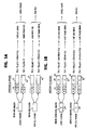
- Fig. 1 illustrates the layer-2 frame format of the present invention.
- the layer-2 frame is composed of a 40-bit normal header and a payload field.
- the normal header of the layer-2 frame contains a length (LEN) field, a frame identifier (FID) field and a frame header error check (FHEC) field.
- the length field is a 2-byte field which is used to indicate the length of the payload and the FID field which is also of 2-byte field to indicate the frame type, payload format and QoS.
- Frame header error check field is a one-byte field, located at the fifth byte from the beginning of the frame, which is the same position as the header error check (HEC) field of ATM cell.
- HEC header error check
- the FHEC held contains the sum of a header CRC sequence computed over all header bits in the LEN and FID fields plus an additional CRC check sequence.
- This additional CRC check sequence is computed over a 127-bit hypothetical header that is composed of an all-zero lower significant bit portion (0-th to 39-th) corresponding to the 40-bit physical header (including the HEC field) and a non-zero higher significant bit portion that extends over the 40-th bit to the 126-th bit.
- the additional CRC sequence is the remainder of division of a 127-bit hypothetical, extended header x i (where i is between the 40-th and 126-th bit of the hypothetical header) by the generator polynomial G(x).
- the CRC result computed over the first four bytes from the beginning of the header in a layer-2 frame differs from the equivalent result computed over the first four bytes of an ATM cell.
- the CRC operates over an "hypothetical header" that extends to 127 bits, with the first 40-bit portion being set to all zeros.
- the i-th bit one of the extended bits, is a "1" as shown in Fig. 1.
- all of the extended bits are set zero as shown in Fig. 2.
- Each of the FHEC and HEC fields are dependent on the results of the CRC on each of these hypothetical headers.
- the hypothetical headers are used only for CRC computation, and they are not transmitted or received.
- modulo (x) will be referred to as M ATM (x) for convenience.
- M ATM (x) is used as a preferred modulo for synchronizing the cell start timing, or cell delineation.
- F FHEC (x) [F(x) * x 8 ] Mod G(x) + M L2F (x)
- M L2F (x) M ATM (x) + [x i ] Mod G(x).
- a receiver can easily distinguish between the two types of hypothetical headers even if layer-2 frames and ATM cells are multiplexed "frame by frame", i.e., asynchronously into a common channel. Since the HEC value is the same as that computed over a normal 40-bit length ATM header, the use of an hypothetical header does not affect standard interfaces.
- the receiver extracts layer-2 frames and ATM cells as shown in Figs. 3A and 3B.
- the receiver performs a CRC process on the received 40-bits header and adds the fixed values M L2F (x) and M ATM (x) to the resultant remainder R(x) to reconstitute an ATM hypothetical header H1 and a layer-2 hypothetical header H2, and then performs an error check on the hypothetical headers to identify the type of header.
- the receiver When receiving an error-free layer-2 frame (L2F) header, as shown in Fig. 3A, the receiver detects an i-th bit error in the ATM hypothetical header H1 from the CRC-based result. Since the i-th bit is not sent through the transport channel, this error should not occur. Therefore, the receiver recognizes it as an uncorrectable error in an ATM hypothetical header. On the other hand, the receiver detects no error in the layer-2 hypothetical header H2, thus recognizing the received header as a layer-2 frame header.
- L2F layer-2 frame
- the receiver When receiving an error-free ATM cell header, the receiver detects an i-th bit error in the layer-2 frame hypothetical header H2. Since this i-th bit is not sent through the transport channel, this error does not occur, The receiver recognizes it as an uncorrectable error in a layer-2 frame hypothetical header. On the other hand, the receiver detects no error in the ATM hypothetical header H1, thus recognizing the received header as an ATM cell header.
- the receiver can detect a correctable one-bit error (i.e., j-th bit error) in the layer-2 hypothetical header H2 and an uncorrectable two-bit error (i.e., i-th and j-th bit errors) in the ATM hypothetical header H1.
- the receiver uses the error-checking result to determine that the received header is for a layer-2 frame and proceeds to correct the bit error.
- the receiver When receiving an ATM cell header with a one-bit error (j-th bit error), the receiver can detect a correctable one-bit error (j-th bit error) in the ATM hypothetical header H1 and an uncorrectable two-bit error (i-th and j-th bit errors) in the layer-2 hypothetical header H2. The receiver uses the error-checking result to determine that the received header is for an ATM cell and proceeds to correct the bit error.
- j-th bit error a correctable one-bit error
- i-th and j-th bit errors uncorrectable two-bit error
- the receiver After the header is identified, the receiver starts looking for the current layer-2/ATM boundary. If the received header is for a layer-2 frame, the receiver can identify the end of the current frame boundary by referring to its LEN field. If it is for an ATM cell, the receiver can find its cell boundary by simply jumping 48 bytes ahead.
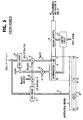
- the logical layer-2 frame assembler includes a 127-bit register 10, in which the layer-2 hypothetical header x i (where "i" is between the 40-th and 126-th bit positions) is stored.
- an input traffic signal is supplied to a control circuit 13 which segments the signal into blocks of appropriate length (with a maximum of 2 16 - 5 bytes) and appends 2-byte length information and a 2-byte frame identifier to each segmented block.
- a shift register 14 is provided, which is segmented into LEN, FID, FHEC and payload fields corresponding to the frame format to store the length information and the frame identifier into the LEN and FID fields, respectively, and the segmented block into the payload field.
- the header error check code F FHEC (x) is formed in an adder 17 by summing together the outputs of division circuit 16 and adder 12 and stored in the FHEC field of the shift register 14. When all the necessary information are stored in the shift register 14, they are forwarded to an asynchronous multiplexer 18.
- Fig. 5 shows a logical structure of an ATM cell assembler.
- the logical ATM cell assembler includes a virtual 127-bit register 20, in which the ATM hypothetical header (i.e., all zero bits) are stored.
- the ATM modulo M ATM (x) is summed in a virtual adder 22 to the zero-output of the virtual division circuit 21.
- an input traffic signal is supplied to a control circuit 23 which formulates a 48-byte payload signal and 4-byte header information (GFC/VPI/VCI/PT/CLP) and stores them into a shift register 24.
- the four-byte cell header information F(x) are multiplied by a bit sequence x 8 in a multiplier 25 and a remainder [F(x) * x 8 ] Mod G(x) is then produced in a division circuit 26 by dividing the output of the multiplier 25 by the generator polynomial G(x).
- the header error check code F HEC (x) is formed in an adder 27 by summing together the outputs of division circuit 26 and virtual adder 22 and stored in the HEC field of the shift register 24.
- the multiplexed bit stream is transmitted over the common channel to a distant receive site where a demultiplexer is provided for distinguishing between layer-2 frames and ATM cells.
- the demultiplexer is shown in Fig. 6.
- the multiplexed bit stream is input to a buffer 30 and a shift controller 31.
- Shift controller 30, which is preset by a length detector 38, counts the number of input bits and decrements the preset value by the count number of the bits stored in the buffer 30.
- Shift controller 31 supplies an output representing the remaining count value to the buffer 30 as a shift control signal.
- the shift controller 31 When the first five-byte header bits from the beginning of a frame/cell boundary are stored in the buffer 30, the shift controller 31 enables a division circuit 32 to divide the five-byte header information (including the header error check code) by the generator polynomial G(x). The remainder R(x) of the division is supplied to adders 33 and 34 where modulo constants M ATM (x) and M L2F (x) are added to the remainder R(x). If no bit error exists, the output of each adder is zero. Otherwise, a non-zero value is produced. Error detectors 35 and 36 examine the outputs of adders 33 and 34 and determines whether an error exists in the header bits. If a correctable error exists, the error detectors identify its bit position, and communicates their results to a decision circuit 37.
- the decision circuit 37 analyzes the outputs of error detectors 35 and 36 and determines whether the header is for a layer-2 frame or an ATM cell depending on the number of bit errors.
- the decision circuit 37 directs an error corrector 39 to correct one-bit error and informs the length detector 38 of the identified frame format. If the header is identified as a frame header, the length detector 38 reads length information from the LEN field of the frame stored in the buffer 30 and directs the shift controller 31 to shift the contents of the buffer 30 by an amount corresponding to the length of the payload field of the frame. If the header is identified as an ATM cell header, the length detector 38 directs the shift controller 31 to shift the contents of the buffer 30 by the fixed value of 48 bytes. The payload bits stored in the buffer 30 are now forwarded through a selector 40 to one of its outputs depending on a control signal supplied from the decision circuit 37.
- Fig. 7 illustrates the transition from an initial state, called "byte hunting state", to the frame synchronized state, called "sync state".
- byte hunting state the decision circuit 37 searches for the boundary with the next layer-2 frame or ATM cell by moving forward one byte at a time.
- the decision circuit supposes that the current incoming byte is the beginning of a new layer-2 frame or ATM cell and then checks the first five-byte sequence from that byte for a match with a valid layer-2 frame or ATM header.
- the decision circuit tentatively supposes that it has found the frame or cell boundary and enters a pre-sync state. Otherwise, it shifts one byte forward and returns to the byte-hunting state. In the pre-sync state, the decision circuit checks the first five bytes from the next boundary. When the decision circuit detects N consecutive layer-2 headers or ATM headers, it enters the sync state. If the decision circuit fails to find the headers before N consecutive headers and detected, it returns to the byte-hunting state. In the sync state, the layer-2 frames/ATM cells are extracted. If an uncorrectable error occurs, the decision circuit leaves the sync state and enters the byte-hunting state.
- Fig. 8 shows details of the operation of the decision circuit 37.
- Frame sync algorithm starts with initialization step 50 in which the count value C for counting N consecutive headers is set to zero.
- the decision circuit checks to see if no ATM error and a one-bit frame error exist. If so, the decision circuit informs the length detector 38 that the header is for an ATM cell and directs the selector 40 to choose the lower output path (step 53). In response, the length detector 38 directs the shift controller 31 to move the contents of the buffer 30 by 48 bytes, so that the header of the next frame/cell is shifted to the position of the shift register 30 to which the division circuit 32 is connected.
- step 51 the routine proceeds to step 52 to check to see if a one-bit ATM error and no frame error exist at the same time. If so, the decision circuit informs the length detector 38 that the header is for a layer-2 frame and directs the selector 40 to choose the upper output path (step 54). In response, the length detector 38 reads length information from the LEN field of the current frame and directs the shift controller 31 to move the contents of the buffer 30 by the length of the payload field, so that the header of the next frame/cell is brought to the position of the shift register 30 to which the division circuit 32 is connected. If the decision at step 52 is negative, flow returns to the starting point of the routine and steps 50, 51 and 52 will be repeated as long as the demultiplexer is in the byte-hunting state.
- step 55 the count value C is incremented by one. Steps 51 to 55 are repeated until the count value C is incremented to N (step 56) as long as the decision circuit is in the pre-sync state.
- step 56 When the count value C is equal to N, it is determined that frame/cell extractions have occurred consecutively N times and flow proceeds from step 56 to step 57.
- the demultiplexer now enters the sync state.
- the decision circuit checks to see if no ATM error and a one-bit frame error exist. If so, the header is for an ATM cell and flow proceeds to step 58 to shift the buffer contents by 48 bytes, forwards them through the selector 40 to the lower data path, and returns to step 57. If the decision at step 57 is negative, the decision circuit tests to see if there is a one-bit ATM error and no frame error exists (step 59).
- step 60 the routine proceeds to step 60 to shift the buffer contents by the payload length of the frame and returns to step 57. As long as the demultiplexer is in the sync state, steps 57 to 60 will be repeatedly executed.
- step 59 If the decision at step 59 is negative, flow proceeds to step 61 to test for the presence of a two-bit ATM error and a one-bit frame error. If this is the case, the header is identified as a layer-2 frame header and the buffer contents are shifted by the length of its payload (step 62) and the decision circuit directs the error corrector 39 to correct the one-bit frame error (step 63), and returns to step 57.
- step 64 test for the presence of a one-bit ATM error and a two-bit frame error. If this is the case, the header is identified as an ATM header and the buffer contents are shifted by 48 bytes (step 65) and the decision circuit directs the error corrector 39 to correct the one-bit ATM error (step 63), and returns to step 57.
- the demultiplexer When the demultiplexer loses synchronism with the incoming bit stream, it returns to the byte-hunting state. In this case, the decision circuit exits from step 64 and returns to the starting point of the routine.
- the layer-2 frame can be formulated in separate locations. In the first location, a layer-2 frame is formulated only with the M ATM (x), which is then transmitted to the second location. In the second location, the remainder [x i ] Mod G(x) ⁇ 0 is summed to the FHEC field of the frame so that the frame can be asynchronously multiplexed with ATM cells.
- the frame assembler can be simplified by eliminating the use of register 10, division circuit 11 and adder 12 of Fig. 4.
- a communication system is illustrated in which a layer-2 frame is initially formulated by a layer-2 frame assembler 70 provided in a first location. The frame is then transmitted through a transmission line 71 to an HEC converter 72 provided in a second location, where the output of the HEC converter 72 is multiplexed with ATM cells by the asynchronous multiplexer 18. The multiplexed signal is transmitted to the demultiplexer of Fig. 6. Details of the communication system of Fig. 9A are shown in Fig. 10.
- the frame assembler 70 is composed of controller 13 which segments an input unformatted bit sequence of PPP frame into a payload signal and produce header information of the payload signal.
- the header information represents the payload length and the frame identifier.
- Controller 13A stores these items of information into respective fields of shift register 14A.
- the information stored in the LEN and FID fields are multiplied by x 8 in multiplier 15A and then divided by G(x) in division circuit 16, in the same manner as described.
- the output of the adder 17A is written into the FHEC field of shift register 14A, forming a layer-2 frame (or type 0), which cannot be statistically multiplexed with other data units such as other layer-2 frames or ATM cells.
- the frame formulated in the shift register 14 is forwarded onto the transmission line 71 and received by the HEC converter 72 where the controller 13B stores the field data of the frame into corresponding fields of shift register 14B except for the header error check code.
- This error check code is supplied to adder 17B and summed with the non-zero hypothetical remainder [x i ] Mod G(x) and then stored in the FHEC field of shift register 14B.
- the layer-2 frame stored in the shift register 14B is converted to the format (or type-1 format) that can be statistically multiplexed with ATM cells or other layer-2 frames whose header error check code is not summed with the non-zero hypothetical remainder.
- the layer-2 frame (type 1) is now forwarded from the HEC converter 72 to asynchronous multiplexer 18A to which ATM cells are also supplied. These signals are statistically multiplexed in a manner as will be described in detail later.
- the HEC converter 72 may be co-located with an ATM cell assembler 73.
- An unformatted signal is supplied to the ATM cell assembler 73.
- the unformatted signal is segmented by a controller 80 into a 48-byte payload signal and inserted to a payload field of a shift register 81 and an ATM header consisting of GFC, VPI, VCI, PT and CLP data is formulated and stored in a 4-byte field of the shift register.
- the 4-byte header information is multiplied by modulo x 8 in a multiplier 82 and divided by the generator polynomial G(x) in a division circuit 83 and summed in an adder 84 to a modulo M ATM (x), producing a header error check code, which is stored in the HEC field of shift register 81 to complete an ATM cell.
- the ATM cell is forwarded to multiplexer 18 where it is multiplexed with layer-2 frames (type 1) from the HEC converter 72 onto a common channel for transmission to the demultiplexer.
- Layer-2 frames of type 1 may be formulated in a single location and multiplexed with ATM cells (Fig. 9C).
- Layer-2 frame assembler 74 shown in Fig. 12, is a combination of the type-0 assembler 70 and HEC converter 72 of Fig. 10 and is identical to that shown in Fig. 4 except that the virtual register 10, division circuit 11 and adder 12 of Fig. 4 are dispensed with.
- Layer-2 frames of type 1 and ATM cells may be formulated and multiplexed together in a single location as shown in Fig. 9D using the frame assembler 74 (Fig. 12) and the ATM assembler 73 (Fig. 11).
- the asynchronous multiplexer 18 is comprised of a pair of buffers 90 and 91, a control unit 92 and a line interface 93.
- Layer-2 frames and ATM cells are stored in the buffers 90 and 91 respectively.
- Control unit 92 constantly examines the presence of cells in the ATM buffer 90 and their contents if present and controls the traffic of layer-2 frames through a control bus 94.
- the operation of the controller 92 proceeds according to a programmed routine shown in Fig. 13.
- the routine starts with decision step 100 to determine whether cells/frames are stored in both of the buffers 90 and 91. If so, flow proceeds to step 101 to examine the header of the cell in buffer 90 and determines whether the cell is classified as a high priority cell. If this is the case, the stored ATM cell is forwarded from the buffer 90 to the line interface 93 for transmission (step 106), and flow returns to the starting point of the routine. If the stored cell is not classified as high priority, the routine proceeds from step 101 to step 102 to check to see if high QoS (Quality-of-Service) parameter is contained in the cell header.
- QoS Quality-of-Service
- control unit 92 proceeds to step 103 and directs the controller 13B of the layer-2 frame assembler 72 to reduce its frame length by setting some upper limit, which is shorter than the average length, on length data inserted into the LEN field.
- step 105 sequentially transmit the currently frame and cell from the buffers 90 and 91, and returns to the starting point of the routine. If no data is stored in both buffers, flow proceeds from step 100 to step 104 in which the controller 92 formulates and transmits idle layer-2 frames by setting their frame length to zero and repeats the process.
- the restriction of frame length imposed by the multiplexer 18 on the frame assembler at step 103 is a back-pressure control action generated in response to the header of cells stored in buffer 90.
- This back-pressure control at step 103 is modified as steps 103A and 103B as shown in Fig. 14.
- a superframe (or hypothetical frame) is defined.
- the controller 92 forwards a plurality of ATM cells from buffer 90 at the start of a superframe (step 103A) and then forwards a plurality of layer-2 frames before the end of the superframe.
- Fig. 15 is a block diagram of a transmission system that incorporates the layer-2 frame assembler, HEC converter, asynchronous multiplexer and demultiplexer of the present invention, in addition to an HEC re-converter which will be described later.
- the transmission system of Fig. 15 includes a frame switch 110 and an ATM switch 130.
- routing information contained in the header of an incoming frame/cell is used for routing the frame/cell to a destination output port.
- One of the input ports 111 of the frame switch receives frames of format which differs from the format of the layer-2 frame of this invention.
- a layer-2 frame assembler 112 is connected to one of the output ports of frame switch 110 to convert the frame arriving on input port 111 to a layer-2 frame of type 1.
- An asynchronous multiplexer 113 combines the output of assembler 112 with ATM cells supplied from the ATM switch 130.
- a first pair of demultiplexers 115 and 116 is provided. Each of these multiplexers supplies a multiplex of frame/cell hybrid signals. The outputs of these multiplexers can be interchanged with other frames/cells through the frame switch 110 and ATM switch 130.
- An ATM cell stream may be applied through port 114 to the ATM switch 130 for routing to the multiplexer 113 or a multiplexer 117.
- ATM cells from the demultiplexers 115 and 116 can be routed through the ATM switch 130 to the multiplexers 113 and 117 where they are multiplexed again with layer-2 frames which are different from those with which they are previously multiplexed.
- Layer-2 frames of type 1 from the demultiplexers 115 and 116 can be routed through the frame switch 110 to the multiplexers 117 and 118 where they are multiplexed again with ATM cells and layer-2 frames of type 0 arriving on port 119.
- a second pair of demultiplexers 120 and 121 supplies a multiplex of layer-2 frames of type 1 and type 0.
- Layer-2 frame of type 1 from the demultiplexer 120 can be multiplexed with the layer-2 frame of type 0 from the demultiplexer 121 in the multiplexer 118
- Layer-2 frames of type 0 from the demultiplexers 120 and 121 can be multiplexed in a multiplexer 123 after converting one of these frames to a type-1 frame in an HEC converter 122
- the layer-2 frames of type 1 from the demultiplexers 120 and 121 can be multiplexed in a multiplexer 125 after converting one of these to a type-0 frame in an HEC re-converter 124 which removes the [x i ] Mod G(x) component from the type-1 in a manner to be described below.
- HEC re-converter 124 provides a process inverse to that the HEC converter since it subtracts the hypothetical modulo component [x i ] Mod G(x) from the layer-2 frame of type 1.
- the HEC re-converter 124 is comprised of a controller 130, a shift register 131 and a subtractor 132.
- Controller 130 stores the field data of a layer-2 frame of type 1 into corresponding fields of shift register 131 except for the header error check code, This error check code is supplied to the subtractor 132, where the non-zero hypothetical remainder [x i ] Mod G(x) is removed and then stored in the FHEC field of shift register 131.
- the frame stored in the shift register 131 is a type-0 layer-2 frame that can be statistically multiplexed with layer-2 frames of type 1 whose header error check code is summed with the non-zero hypothetical remainder.
Landscapes
- Engineering & Computer Science (AREA)
- Computer Networks & Wireless Communication (AREA)
- Signal Processing (AREA)
- Detection And Prevention Of Errors In Transmission (AREA)
- Data Exchanges In Wide-Area Networks (AREA)
- Time-Division Multiplex Systems (AREA)
Applications Claiming Priority (2)
| Application Number | Priority Date | Filing Date | Title |
|---|---|---|---|
| JP2000035584 | 2000-02-14 | ||
| JP2000035584 | 2000-02-14 |
Publications (2)
| Publication Number | Publication Date |
|---|---|
| EP1126652A2 true EP1126652A2 (fr) | 2001-08-22 |
| EP1126652A3 EP1126652A3 (fr) | 2009-02-25 |
Family
ID=18559760
Family Applications (1)
| Application Number | Title | Priority Date | Filing Date |
|---|---|---|---|
| EP01102886A Withdrawn EP1126652A3 (fr) | 2000-02-14 | 2001-02-14 | Procédé et système de transmission et réception de signaux multiplexés de façon asynchrone |
Country Status (3)
| Country | Link |
|---|---|
| US (2) | US7126950B2 (fr) |
| EP (1) | EP1126652A3 (fr) |
| CA (1) | CA2335898A1 (fr) |
Cited By (2)
| Publication number | Priority date | Publication date | Assignee | Title |
|---|---|---|---|---|
| EP2141849A3 (fr) * | 2008-06-30 | 2013-12-18 | Fujitsu Limited | Système de transmission et de réception de paquets avec un code de vérification d'erreur |
| RU2622853C2 (ru) * | 2013-03-20 | 2017-06-20 | Фраунхофер-Гезелльшафт Цур Фердерунг Дер Ангевандтен Форшунг Е.Ф. | Двухэтапная сигнализация для передачи потока данных |
Families Citing this family (6)
| Publication number | Priority date | Publication date | Assignee | Title |
|---|---|---|---|---|
| WO2003017556A2 (fr) * | 2001-08-15 | 2003-02-27 | Acterna Llc | Module de telecommande pour un reseau de telecommunication |
| US10785316B2 (en) | 2008-11-24 | 2020-09-22 | MeshDynamics | Evolutionary wireless networks |
| US8514852B2 (en) * | 2008-11-24 | 2013-08-20 | Mesh Dynamics, Inc. | Real time packet transforms to avoid re-transmission |
| US20090249172A1 (en) * | 2008-03-26 | 2009-10-01 | Qualcomm Incorporated | Methods and apparatus for improved decoding of bursts that include multiple concatenated protocol data units |
| US8126014B2 (en) * | 2008-04-09 | 2012-02-28 | Qualcomm Incorporated | Methods and apparatus for improved decoding of hybrid automatic repeat request transmissions |
| US8989330B2 (en) * | 2010-07-30 | 2015-03-24 | Silicon Laboratories Inc. | Method and apparatus to detect a synchronization delimiter |
Citations (1)
| Publication number | Priority date | Publication date | Assignee | Title |
|---|---|---|---|---|
| EP0366589A2 (fr) | 1988-10-27 | 1990-05-02 | International Business Machines Corporation | Méthode pour maintenir l'intégrité des données durant la transmission de messages dans un système de communication de données |
Family Cites Families (14)
| Publication number | Priority date | Publication date | Assignee | Title |
|---|---|---|---|---|
| GB9312135D0 (en) * | 1993-06-11 | 1993-07-28 | Inmos Ltd | Generation of checking data |
| JPH0787090A (ja) * | 1993-06-30 | 1995-03-31 | Toyo Commun Equip Co Ltd | 巡回符号検出方法及び装置 |
| JP3405800B2 (ja) * | 1994-03-16 | 2003-05-12 | 富士通株式会社 | Atmによる可変長セルの転送方式,atmによる可変長セルのスイッチ及びatmによる可変長セルの交換機 |
| US5434719A (en) * | 1994-03-18 | 1995-07-18 | Seagate Technology, Inc. | Correction of header information in a magnetic disc drive |
| US5771249A (en) * | 1994-09-02 | 1998-06-23 | Toyo Communication Equipment Co., Ltd. | ATM cell synchronous system |
| US5600653A (en) * | 1994-09-30 | 1997-02-04 | Comsat Corporation | Technique for improving asynchronous transfer mode operation over a communications link with bursty bit errors |
| EP0719065A1 (fr) * | 1994-12-20 | 1996-06-26 | International Business Machines Corporation | Noeud de communication de paquets polycalent pour un réseau de communication de données |
| FR2735889B1 (fr) * | 1995-06-22 | 1997-09-05 | Sgs Thomson Microelectronics | Circuit de calcul de syndrome |
| DE69731932T2 (de) * | 1996-10-29 | 2006-02-16 | International Business Machines Corp. | Verfahren und Vorrichtung für zweistufige CRC-32-Berechnung |
| KR100211918B1 (ko) * | 1996-11-30 | 1999-08-02 | 김영환 | 비동기식전송모드셀 경계 식별장치 |
| US6038694A (en) * | 1997-03-24 | 2000-03-14 | Cisco Systems, Inc. | Encoder for producing a checksum associated with changes to a frame in asynchronous transfer mode systems |
| US6317433B1 (en) * | 1997-10-16 | 2001-11-13 | Cisco Technology, Inc. | Method and system for optimizing transmission link bandwidth occupation in high speed digital networks |
| EP1005780B1 (fr) * | 1998-06-19 | 2012-05-02 | Juniper Networks, Inc. | Procede et dispositif permettant d'encapsuler/desencapsuler des donnees canal par canal au niveau du materiel |
| US6331978B1 (en) * | 1999-03-09 | 2001-12-18 | Nokia Telecommunications, Oy | Generic label encapsulation protocol for carrying label switched packets over serial links |
-
2001
- 2001-02-13 CA CA002335898A patent/CA2335898A1/fr not_active Abandoned
- 2001-02-13 US US09/782,879 patent/US7126950B2/en not_active Expired - Fee Related
- 2001-02-14 EP EP01102886A patent/EP1126652A3/fr not_active Withdrawn
-
2006
- 2006-05-01 US US11/414,415 patent/US20060193325A1/en not_active Abandoned
Patent Citations (1)
| Publication number | Priority date | Publication date | Assignee | Title |
|---|---|---|---|---|
| EP0366589A2 (fr) | 1988-10-27 | 1990-05-02 | International Business Machines Corporation | Méthode pour maintenir l'intégrité des données durant la transmission de messages dans un système de communication de données |
Non-Patent Citations (1)
| Title |
|---|
| D.R. IRVIN: "Preserving the integrity of cyclic redundancy checks when protected text is intentionally altered", IBM JOURNAL OF RESEARCH AND DEVELOPMENT, vol. 33, no. 6, pages 618 - 626 |
Cited By (3)
| Publication number | Priority date | Publication date | Assignee | Title |
|---|---|---|---|---|
| EP2141849A3 (fr) * | 2008-06-30 | 2013-12-18 | Fujitsu Limited | Système de transmission et de réception de paquets avec un code de vérification d'erreur |
| RU2622853C2 (ru) * | 2013-03-20 | 2017-06-20 | Фраунхофер-Гезелльшафт Цур Фердерунг Дер Ангевандтен Форшунг Е.Ф. | Двухэтапная сигнализация для передачи потока данных |
| US10057013B2 (en) | 2013-03-20 | 2018-08-21 | Fraunhofer-Gesellschaft Zur Foerderung Der Angewandten Forschung E.V. | Two-stage signaling for transmission of a datastream |
Also Published As
| Publication number | Publication date |
|---|---|
| US7126950B2 (en) | 2006-10-24 |
| CA2335898A1 (fr) | 2001-08-14 |
| US20060193325A1 (en) | 2006-08-31 |
| US20010046232A1 (en) | 2001-11-29 |
| EP1126652A3 (fr) | 2009-02-25 |
Similar Documents
| Publication | Publication Date | Title |
|---|---|---|
| US5570362A (en) | System for transferring variable length cells under ATM | |
| US20060193325A1 (en) | Method and system for transmission and reception of asynchronously multiplexed signals | |
| US6108336A (en) | AAL-5 SSCS for AAL-1 and AAL-2 in ATM networks | |
| US7386008B2 (en) | Method and apparatus for converting data packets between a higher bandwidth network and a lower bandwidth network having multiple channels | |
| JP2000512105A (ja) | ミニセル・シーケンス番号カウント | |
| US6034954A (en) | Multiplexing apparatus for transit of signals between service provided by low-speed transmission path and ATM service provided by high-speed transmission path | |
| JP2002077243A (ja) | セル/パケット混在の伝送方法および伝送装置 | |
| CN100493075C (zh) | 变长数据分组与定长信元混合传送的方法与适配装置 | |
| JP2001103091A (ja) | 伝送方法およびネットワーク・システム | |
| US6442163B1 (en) | Depacketizer and a frame aligner including the depacketizer | |
| US6973084B1 (en) | Hybrid data transport scheme over optical networks | |
| US6272138B1 (en) | Method and apparatus for reducing jitter or wander on internetworking between ATM network and PDH network | |
| JP3539551B2 (ja) | 共通搬送波上への異種データトラヒック収容フレーム及び伝送装置 | |
| GB2324443A (en) | Multiplex transmission arrangement | |
| JP4219408B2 (ja) | 柔軟なフレーム構造を有する送信システム | |
| JP3245333B2 (ja) | Cbr信号の位相跳躍防止方式 | |
| US5978361A (en) | ATM digital radio transmission method and system therefor | |
| JPH11284641A (ja) | エラ―補正回路 | |
| JP3539556B2 (ja) | 共通搬送波上への異種クライアントデータ転送方法及びatm/フレーム多重化伝送装置及びルータ構成 | |
| JPH09298545A (ja) | Atmデジタル無線伝送方法及びそのシステム | |
| EP1407565B1 (fr) | Procede et appareil pour convertir des paquets de donnees entre un reseau a bande large et un reseau presentant une largeur de bande inferieure | |
| US6694472B1 (en) | Error correction for frames carried over multiple networks | |
| JP2919214B2 (ja) | Atm通信方式における0/1系無瞬断切替方式 | |
| KR0134433B1 (ko) | 광대역종합통신망에 있어서 셀 헤더부의 셀 기준신호 복원방법 | |
| JP4292687B2 (ja) | 通信装置及びネットワーク |
Legal Events
| Date | Code | Title | Description |
|---|---|---|---|
| PUAI | Public reference made under article 153(3) epc to a published international application that has entered the european phase |
Free format text: ORIGINAL CODE: 0009012 |
|
| AK | Designated contracting states |
Kind code of ref document: A2 Designated state(s): AT BE CH CY DE DK ES FI FR GB GR IE IT LI LU MC NL PT SE TR |
|
| AX | Request for extension of the european patent |
Free format text: AL;LT;LV;MK;RO;SI |
|
| PUAL | Search report despatched |
Free format text: ORIGINAL CODE: 0009013 |
|
| AK | Designated contracting states |
Kind code of ref document: A3 Designated state(s): AT BE CH CY DE DK ES FI FR GB GR IE IT LI LU MC NL PT SE TR |
|
| AX | Request for extension of the european patent |
Extension state: AL LT LV MK RO SI |
|
| 17P | Request for examination filed |
Effective date: 20090202 |
|
| AKX | Designation fees paid |
Designated state(s): DE FR |
|
| 17Q | First examination report despatched |
Effective date: 20091103 |
|
| STAA | Information on the status of an ep patent application or granted ep patent |
Free format text: STATUS: THE APPLICATION IS DEEMED TO BE WITHDRAWN |
|
| 18D | Application deemed to be withdrawn |
Effective date: 20110901 |