EP1122608A2 - Projektionsbelichtungsanlage mit reflektivem Retikel - Google Patents
Projektionsbelichtungsanlage mit reflektivem Retikel Download PDFInfo
- Publication number
- EP1122608A2 EP1122608A2 EP01100542A EP01100542A EP1122608A2 EP 1122608 A2 EP1122608 A2 EP 1122608A2 EP 01100542 A EP01100542 A EP 01100542A EP 01100542 A EP01100542 A EP 01100542A EP 1122608 A2 EP1122608 A2 EP 1122608A2
- Authority
- EP
- European Patent Office
- Prior art keywords
- beam splitter
- projection exposure
- exposure system
- lens
- illumination
- Prior art date
- Legal status (The legal status is an assumption and is not a legal conclusion. Google has not performed a legal analysis and makes no representation as to the accuracy of the status listed.)
- Granted
Links
- 230000009467 reduction Effects 0.000 claims abstract description 56
- 238000005286 illumination Methods 0.000 claims abstract description 54
- 238000003384 imaging method Methods 0.000 claims abstract description 46
- 230000003287 optical effect Effects 0.000 claims abstract description 45
- 238000001393 microlithography Methods 0.000 claims abstract description 9
- 230000010287 polarization Effects 0.000 claims description 56
- 238000012937 correction Methods 0.000 claims description 7
- 238000004519 manufacturing process Methods 0.000 claims description 4
- 238000000034 method Methods 0.000 claims description 2
- 230000008569 process Effects 0.000 claims description 2
- 239000000758 substrate Substances 0.000 claims 1
- 238000013461 design Methods 0.000 abstract description 22
- 230000008878 coupling Effects 0.000 abstract description 10
- 238000010168 coupling process Methods 0.000 abstract description 10
- 238000005859 coupling reaction Methods 0.000 abstract description 10
- 230000004075 alteration Effects 0.000 abstract description 4
- VYPSYNLAJGMNEJ-UHFFFAOYSA-N Silicium dioxide Chemical compound O=[Si]=O VYPSYNLAJGMNEJ-UHFFFAOYSA-N 0.000 description 77
- 229910052681 coesite Inorganic materials 0.000 description 38
- 229910052906 cristobalite Inorganic materials 0.000 description 38
- 239000000377 silicon dioxide Substances 0.000 description 38
- 235000012239 silicon dioxide Nutrition 0.000 description 38
- 229910052682 stishovite Inorganic materials 0.000 description 38
- 229910052905 tridymite Inorganic materials 0.000 description 38
- 235000012431 wafers Nutrition 0.000 description 20
- 230000005540 biological transmission Effects 0.000 description 9
- 210000001747 pupil Anatomy 0.000 description 6
- IJGRMHOSHXDMSA-UHFFFAOYSA-N Atomic nitrogen Chemical compound N#N IJGRMHOSHXDMSA-UHFFFAOYSA-N 0.000 description 4
- 239000000463 material Substances 0.000 description 4
- 229910004261 CaF 2 Inorganic materials 0.000 description 3
- 201000009310 astigmatism Diseases 0.000 description 3
- 230000008901 benefit Effects 0.000 description 3
- WUKWITHWXAAZEY-UHFFFAOYSA-L calcium difluoride Chemical compound [F-].[F-].[Ca+2] WUKWITHWXAAZEY-UHFFFAOYSA-L 0.000 description 3
- 229910001634 calcium fluoride Inorganic materials 0.000 description 3
- 239000007789 gas Substances 0.000 description 3
- 239000011521 glass Substances 0.000 description 3
- 239000013078 crystal Substances 0.000 description 2
- 238000009826 distribution Methods 0.000 description 2
- 239000001307 helium Substances 0.000 description 2
- 229910052734 helium Inorganic materials 0.000 description 2
- SWQJXJOGLNCZEY-UHFFFAOYSA-N helium atom Chemical compound [He] SWQJXJOGLNCZEY-UHFFFAOYSA-N 0.000 description 2
- 238000001459 lithography Methods 0.000 description 2
- 230000000873 masking effect Effects 0.000 description 2
- 229910052757 nitrogen Inorganic materials 0.000 description 2
- 238000000926 separation method Methods 0.000 description 2
- 206010010071 Coma Diseases 0.000 description 1
- 241000022563 Rema Species 0.000 description 1
- 229910004298 SiO 2 Inorganic materials 0.000 description 1
- 238000010521 absorption reaction Methods 0.000 description 1
- 230000009471 action Effects 0.000 description 1
- 230000006978 adaptation Effects 0.000 description 1
- 239000012876 carrier material Substances 0.000 description 1
- 230000001427 coherent effect Effects 0.000 description 1
- 230000006735 deficit Effects 0.000 description 1
- 230000001419 dependent effect Effects 0.000 description 1
- 230000000694 effects Effects 0.000 description 1
- 238000001900 extreme ultraviolet lithography Methods 0.000 description 1
- 210000000887 face Anatomy 0.000 description 1
- 239000011888 foil Substances 0.000 description 1
- 238000010884 ion-beam technique Methods 0.000 description 1
- 238000013507 mapping Methods 0.000 description 1
- 239000000203 mixture Substances 0.000 description 1
- 238000005498 polishing Methods 0.000 description 1
- 238000012545 processing Methods 0.000 description 1
- 230000005855 radiation Effects 0.000 description 1
- 230000011514 reflex Effects 0.000 description 1
- 239000004065 semiconductor Substances 0.000 description 1
- 238000011144 upstream manufacturing Methods 0.000 description 1
Images



Classifications
-
- G—PHYSICS
- G03—PHOTOGRAPHY; CINEMATOGRAPHY; ANALOGOUS TECHNIQUES USING WAVES OTHER THAN OPTICAL WAVES; ELECTROGRAPHY; HOLOGRAPHY
- G03F—PHOTOMECHANICAL PRODUCTION OF TEXTURED OR PATTERNED SURFACES, e.g. FOR PRINTING, FOR PROCESSING OF SEMICONDUCTOR DEVICES; MATERIALS THEREFOR; ORIGINALS THEREFOR; APPARATUS SPECIALLY ADAPTED THEREFOR
- G03F7/00—Photomechanical, e.g. photolithographic, production of textured or patterned surfaces, e.g. printing surfaces; Materials therefor, e.g. comprising photoresists; Apparatus specially adapted therefor
- G03F7/70—Microphotolithographic exposure; Apparatus therefor
- G03F7/70058—Mask illumination systems
- G03F7/70066—Size and form of the illuminated area in the mask plane, e.g. reticle masking blades or blinds
-
- G—PHYSICS
- G03—PHOTOGRAPHY; CINEMATOGRAPHY; ANALOGOUS TECHNIQUES USING WAVES OTHER THAN OPTICAL WAVES; ELECTROGRAPHY; HOLOGRAPHY
- G03F—PHOTOMECHANICAL PRODUCTION OF TEXTURED OR PATTERNED SURFACES, e.g. FOR PRINTING, FOR PROCESSING OF SEMICONDUCTOR DEVICES; MATERIALS THEREFOR; ORIGINALS THEREFOR; APPARATUS SPECIALLY ADAPTED THEREFOR
- G03F7/00—Photomechanical, e.g. photolithographic, production of textured or patterned surfaces, e.g. printing surfaces; Materials therefor, e.g. comprising photoresists; Apparatus specially adapted therefor
- G03F7/70—Microphotolithographic exposure; Apparatus therefor
- G03F7/70216—Mask projection systems
- G03F7/70225—Optical aspects of catadioptric systems, i.e. comprising reflective and refractive elements
-
- G—PHYSICS
- G03—PHOTOGRAPHY; CINEMATOGRAPHY; ANALOGOUS TECHNIQUES USING WAVES OTHER THAN OPTICAL WAVES; ELECTROGRAPHY; HOLOGRAPHY
- G03F—PHOTOMECHANICAL PRODUCTION OF TEXTURED OR PATTERNED SURFACES, e.g. FOR PRINTING, FOR PROCESSING OF SEMICONDUCTOR DEVICES; MATERIALS THEREFOR; ORIGINALS THEREFOR; APPARATUS SPECIALLY ADAPTED THEREFOR
- G03F7/00—Photomechanical, e.g. photolithographic, production of textured or patterned surfaces, e.g. printing surfaces; Materials therefor, e.g. comprising photoresists; Apparatus specially adapted therefor
- G03F7/70—Microphotolithographic exposure; Apparatus therefor
- G03F7/70216—Mask projection systems
- G03F7/70283—Mask effects on the imaging process
Definitions
- the invention relates to a projection exposure system with a reticle that is in reflection is operated.
- Lithography with soft X-rays is used exclusively with reflective reticles worked.
- the beam division of lighting and imaging Beam path is realized by oblique incidence of the lighting.
- Beam splitter cube or Beam splitter plates are not used.
- the lenses are pure mirror lenses with non-axially symmetrical beam path.
- the oblique incidence of the illuminating light on the The disadvantage of reflective reticles is that the raised mask bridges lead to vignetting.
- JP-A 9-017719 is a wafer projection exposure system with a reflex LCD as known special reticle.
- a flat beam splitter plate for Separation of lighting and imaging beam path used. Lighting system and projection lens with a field symmetrical to the optical axis operated.
- the coupling of the illuminating light directly in front of a beam splitter plate the reticle corresponding to JP-A 9-017719 requires the corresponding one Input focal length, on the other hand, the passage through the flat plate leads to astigmatic deformation of the illuminating light beam, which the required clean Pupil imaging disturbs.
- a catadioptric microscope objective is known from US Pat. No. 5,956,174 a beam splitter cube between microscope objective and tube lens the illuminating light is coupled. This type of illumination is quite common in incident light microscopes. The illuminated field sizes are only in the order of 0.5 mm.
- Catadioptric systems for the wavelengths 193 nm and 157 nm are known. So give the published documents DE 44 17 489 A1 (US ser. no. 08/583 025) and DE 196 16 922 A1 (US ser. No. 08/845 384) by the applicant catadioptric projection lenses with Beam splitter cube without an intermediate image.
- Catadioptric projection lenses with beam splitter cubes and intermediate image are the pending application DE 199 54 727.0 entitled “Catadioptric lens with physical beam splitters and intermediate image ".
- transmission reticles that is to say masks for microlithography operated in transmission
- the materials CaF 2 or MgF 2 are conceivable.
- reticles made of CaF 2 or MgF 2 are difficult to process and therefore very expensive.
- absorption and the resulting thermal expansion of the reticle in multiple exposures reduce the minimum structure size that can be applied to a semiconductor chip. If possible, materials such as MgF 2 are avoided because they are also birefringent.
- the alternative is reflective reticles.
- the projection lens is designed as a reduction lens and that The reticle is scaled down. Then the reticle can be provided with larger structures.
- the typical input focal length of e.g. 30 mm prevents that Illumination at suitable angles of incidence.
- the object of the invention is therefore projection exposure systems with a reduction lens to be specified which result in perfect function with a reflective reticle.
- a projection exposure system of microlithography according to claim 1, wherein a beam splitter cube for superimposing lighting and Imaging beam path serves.
- This allows numerous lens design concepts for Adapt reflective reticle, as the following examples show.
- a Beam splitter cubes instead of a plane-parallel beam splitter plate are error entries of the Avoided beam splitter plate operated at 45 °.
- the lighting system should be designed according to claim 4 so that the Illumination beam path with deviations less than ⁇ 2.5mrad in the imaging Beam path passes. This deviation can be measured by looking for the heavy beams after the reflection on the reticle, the angles with respect to the reticle plane are determined and the Deviation from the angles of the corresponding main rays is calculated.
- the angles of the heavy beams depend on the radiation characteristics of the light source and the design of the Lighting system, the angles of the main rays exclusively from the design of the Reduction objective dependent.
- a polarization beam splitter cube is used according to claim 5.
- the illuminating light must be more than 95% linearly polarized his.
- the direction of polarization depends on whether the illumination beam path on the Beam splitter layer should be reflected or not. In the case of reflection, this must be done
- Illumination light must be polarized parallel to the beam splitter surface, in the case of transmission perpendicular to the beam splitter surface.
- Claims 6-10 relate to embodiments in which the beam splitter cube is used exclusively for coupling the illumination beam path.
- the beam splitter cube is advantageous to divide the reduction lens into two sub-lenses, with a first one Intermediate image with a magnification of -1.0 ⁇ 0.25 and a second one Image with a magnification of -0.25 ⁇ 0.15.
- the beam splitter cube will be there integrated into the first intermediate image.
- the second figure can be purely refractive or be catadioptric.
- the coupling of the illumination beam path with a is particularly advantageous Beam splitter cube if the beam splitter cube according to claims 11-13 already Is part of the reduction lens. Then the fourth unused side of the Beam splitter cubes can be used to couple the illumination beam path.
- a catadioptric lens has a deflecting mirror, it can Deflecting mirror can be replaced by a beam splitter cube, over which the illuminating light is coupled.
- the design of the catadioptric lens can be carried out with and without an intermediate image his.
- the task is performed by a projection exposure system according to the claims 17 to 23 solved, in which a special beam splitter plate is provided, which in Illumination beam path in the passage, operated reflectively in the imaging beam path becomes. Reflection is provided in air, i.e. in the optically thinner medium that also vacuum or a special gas mixture or a gas, e.g. Nitrogen or helium, can be.
- the beam splitter plate is designed so that astigmatic errors due to slanted plate can be corrected refractive.
- a common inventive idea is that the imaging beam path is free of Interference is kept by the beam splitter arrangement and the illuminating beam path is corrected directly by the beam splitter arrangement with lower requirements.
- a beam splitter cube only rotationally symmetrical image errors are introduced that within the lighting system by means of rotationally symmetrical optical elements, e.g. spherical lenses can be corrected.
- the inventive beam splitter plate the correction of the illumination beam path through the special execution of the Lighting system facing side of the beam splitter plate.
- the beam splitter plate is not plan with one Provide correction area. Due to the inclined position of the beam splitter plate, the Correction surface no rotational symmetry, but a simple symmetry with respect to the Meridional level on.
- the beam splitter plate is according to Claim 18 wedge-shaped.
- a beam splitter plate is particularly useful if it meets the requirements 20 instead of a deflection mirror provided in the design of the reduction lens occurs.
- the claims 21-23 treat advantageous embodiments for the use of Beam splitter plate.
- Claim 24 specifies a manufacturing process for microlithographic components, which by Use of a projection exposure system according to one of the preceding claims is marked.
- the overlapping of illumination and projection optics according to the invention enables especially at operating wavelengths in the range of 100-200nm reflective reticles. This avoids the difficulties involved in the production of Transmission reticle by processing the transparent at these wavelengths Materials occur.
- Fig. 1 shows a reduction lens with a reflective reticle and a Beam splitter cube for coupling the illuminating light.
- Fig. 2 shows a reduction lens with upstream intermediate image, in which the Beam splitter cube for coupling the lighting is integrated.
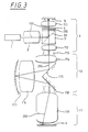
- FIG. 3 shows a kadadioptric reduction lens with an intermediate image in front, in which the beam splitter cube is integrated for coupling the lighting.
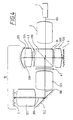
- Fig. 4 shows a cadadioptric reduction lens without intermediate image, the Illumination beam path over the beam splitter cube of the catadioptric Reduction lens is coupled.
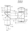
- the Lighting is coupled in via a beam splitter plate at the location of the deflection.
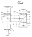
- the Lighting is coupled in via a beam splitter cube at the location of the deflection.
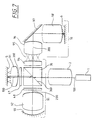
- FIG. 7 shows a cadadioptric reduction lens with an intermediate image, the Illumination over the beam splitter cube of the catadioptric reduction lens is coupled.
- FIG. 8 shows an exemplary embodiment for a catadioptric reduction lens Beam splitter cube and intermediate picture.
- the reflective reticle 5 is made smaller Image with a typical imaging scale ⁇ of -0.25 ⁇ 0.15 on the wafer 6 pictured.
- the illuminated field on the wafer 6 has a diameter of at least 10mm. Rectangular fields with an x-y aspect ratio of are typical 1: 1 to 1: 4.
- the numerical aperture on the image side is greater than 0.5.
- the illustration is done via the optical elements 71 and 72.
- To illuminate the reflective reticle 5 is in the Imaging beam path 200 of the reduction lens between reflective reticle 5 and Wafer 6 a beam splitter cube 3 integrated. It can e.g.
- a polarization beam splitter cube 3 act in which there is a layer system between the prism surfaces is located, the light polarized parallel to the beam splitter surface 30 almost completely is reflected, but is transparent to light polarized perpendicular to the beam splitter surface 30. It is therefore a prerequisite for the arrangement according to FIG. That the illuminating light is polarized parallel to the plane of incidence of the beam splitter surface 30 attached at 45 °. Such polarized light is reflected on the beam splitter surface 30 and in the direction reflective reticle 5 deflected. Is between beam splitter cube 3 and reflective reticle 5 a ⁇ / 4 plate 4 attached, which is run through twice in total.
- the circularly polarized light runs in the imaging Beam path 200 a second time through the ⁇ / 4 plate 4 and is now linear again polarized.
- the direction of polarization is now perpendicular to the beam splitter surface 30 of the Beam splitter cube 3 aligned so that the beam splitter cube 3 without reflection is going through.
- a plane-parallel beam splitter plate would have 3 compared to the polarization beam splitter cube Disadvantage that finite thickness is not due to the beam splitter plate placed at 45 ° rotationally symmetrical aberrations would be introduced.
- the polarization beam splitter cube 3 should be on within the imaging beam path 200 be arranged at a point at which the beams striking the beam splitter surface 30 show little divergence. This is the case when the polarization beam splitter cube 3 is in a location with an almost collimated beam path. There are therefore optical ones between reflective reticle 5 and polarization beam splitter cube 3 To provide elements 71 with an overall positive refractive power that the coming from the reticle essentially collimate divergent light beams.
- the optical elements 72 can be designed differently depending on the design type, but also have overall positive refractive power to move the image to a possible intermediate image level or to the image To achieve wafer level 6.
- Optical elements 71 and 72 can be taken together as refractive elements Present a reduction lens with a typical magnification ⁇ of -0.25 ⁇ 0.15. in the The design of this refractive lens is then between the optical elements 71 and optical elements 72 to provide the ⁇ / 4 plate 4 and the beam splitter cube 3.
- the reflective reticle 5 is illuminated with the aid of the illumination system 2, the Beam splitter cube 3, the ⁇ / 4 plate 4, and the optical elements 71 in the design of the Lighting system 2 must be taken into account.
- the interface between Illumination system 2 and imaging optics is therefore not the reticle 5, as in the case of a transmission reticle or with oblique illumination of the reticle, but rather the entrance of the beam splitter cube 3 facing the lighting system 2.
- the main beam angles with respect to the reticle plane are smaller than ⁇ 15mrad, i.e. the reticle 5 is illuminated almost telecentrically.
- the main rays are like this in the reduction lens defines that they intersect the optical axis at the location of the system aperture.
- the main beam angles make the design of the illumination optics 2 more difficult in that the Heavy rays of the illumination beam path 100 in the reticle plane 5 into the Main rays of the imaging beam path 200 must pass. Due to the Reflection on the reticle, the angle of incidence of the heavy rays must be the opposite Sign like the main rays.
- the illumination beam path is 100 different from the imaging beam path 200 within the optical components 71.
- the distribution of the main beam angles over the illuminated field must be from Lighting system 2 are overcompensated. Since the main beam angle distribution on Reticle 5 is mainly determined by the optical elements 71 and these optical Elements 71 for the design of the lighting system 2 are predefined in the Lighting system 2 optical components - for example a sequence of collecting and diverging lenses - which provide the beam angles on the reticle 5 influence.
- the optical components in the lighting system 2 are designed so that the Heavy rays of the illumination beam path 100 after the reflection on the reflective Reticle 5 depending on the field height with those specified by the design of the reduction lens Main rays coincide up to a maximum angular deviation of ⁇ 2.5 mrad. Otherwise, the telecentricity normally required in wafer level 6 would be violated become.
- the lighting system 2 must have a device for changing the polarization state of the illuminating light included.
- the source 1 With linearly polarized light, the source 1 must if necessary the direction of polarization e.g. about birefringent crystals or birefringent foils can be rotated.
- Polarizers for generating parallel or perpendicular to the beam splitter surface 30 Polarized light can be used. These components are preferred for Influencing the polarization state immediately before the polarization beam splitter cube 3 attached.
- the direction of polarization depends on whether the Illumination beam path 100 is to be reflected on the beam splitter layer 30 or not. In the case of reflection e.g. the illuminating light must be parallel to the beam splitter surface 30 be polarized.
- the lighting system 2 usually contains for homogeneous illumination of the Reticle level 5 integrators, e.g. Honeycomb condensers, waveguides or glass rods.
- the lighting system can be varied by 2 zoom optics, axicon elements, Filter plates in pupil planes, masking devices in pupil or Intermediate field levels may be provided. The functioning of these elements is e.g. in the Patent application DE 195 20 563 A1 described by the applicant.
- Lenses within the Lighting system 2 for adjusting the beam angle of the Illumination beam path 100 to the main beam angle of the reduction lens, that is to say Correct illumination of the entrance pupil of the reduction lens are as REMA lenses known from DE 196 53 983 A1 or DE 195 48 805 A1.
- a DUV or VUV laser can be used as light source 1, for example an ArF laser for 193 nm, an F 2 laser for 157 nm, an Ar 2 laser for 126 nm and a NeF laser for 109 nm.
- the imaging system 7-8 in FIG. 2 has an intermediate image plane 103.
- the illumination light is coupled in via the polarization beam splitter cube 3 with the subsequent ⁇ / 4 plate 4 within the intermediate imaging optics 7.
- the optical elements 101 and 102 each have positive refractive power, the polarization beam splitter cube 3 being in one area with an almost collimated beam path.
- the reduction lens is divided into the intermediate imaging system 7 and the reduction system 8. This has the advantage that space for the polarization beam splitter cube 3 can be created in the intermediate imaging system 7.
- the optical elements 101, the ⁇ / 4 plate 4, and the beam splitter cube 3 must be included in the design of the lighting system 2. It is advantageous if the intermediate image 7 is designed such that the reflective reticle 5 is illuminated almost telecentrically. The incidence angles of the main rays on the reflective reticle 5 should be less than 15 mrad.
- FIG. 3 shows a further embodiment of the invention Projection exposure system for microlithography.
- the picture between reflective Reticle 5 and wafer level 6 take place with two intermediate image planes 113 and 118 Intermediate image 9 from reflective reticle 5 to intermediate image plane 113 is similar constructed like the intermediate imaging system 7 in Fig. 2.
- the mapping of Intermediate image plane 113 on the wafer 6 is first carried out with the aid of the catadioptric Intermediate imaging system 10 and a subsequent refractive reduction system 11.
- the catadioptric intermediate imaging system 10 consists of the optical elements 114, a deflecting mirror 115, the optical elements 116 and the concave mirror 117.
- the object field of the Intermediate imaging system 10 is not centered on the optical axis, but outside the optical axis. In this case, this means that subsystems 10 and 11 are offset to Subsystem 9 must be arranged.
- the numerical aperture on the image side can be used for these Projection lenses have values in the range of 0.65 to 0.8 or more. Are there Field sizes in wafer level 6 in the range from 20mm x 7mm to 30mm x 10mm possible. Such lenses are described in the pending application EP 99 112 539 by the applicant (US ser. no. 09/364 382).
- the coupling of the illumination beam path 100 into the is particularly advantageous imaging beam path 200 if already in the imaging beam path 200 a beam splitter cube is provided, as is the case with some types of catadioptric lenses Case is.
- Catadioptric lens types with beam splitter cubes are different Embodiments known.
- Fig. 4 shows a possible catadioptric projection lens with beam splitter cube 31, the is set up without intermediate images.
- Such lenses consist of reticle 5 a first lens group 121, a deflection mirror 122, a second lens group 123, the beam splitter cube 31, a third lens group 124, a concave mirror 125, one fourth lens group 126 and an aperture that is between the elements 123 and 126 is arranged.
- An image magnification ⁇ of -0.25 ⁇ 0.15 is conceivable for these lenses, an image-side numerical aperture> 0.5 and an image field diameter> 10 mm, preferably> 20 mm.
- the first lens group 121 and the second lens group 123 can be designed so that the divergence of the beams on the beam splitter surface 310 of the Polarization beam splitter cube 31 is minimized. If you consider an edge ray that is from an object point on the optical axis, the sine of the angle can be this Beam with respect to the optical axis through the first and second lens groups 121 and 123 can be reduced by up to 40%. To make a concave with the concave mirror 125 To achieve sufficient color correction, lens group 124 must have a negative refractive power exhibit. The lens group 126 forms the image in the wafer plane 6 and therefore points a positive refractive power.
- the reduction lens 12 shown in FIG. 4 consists of the optical elements 121, 122, 123, 124, 125, 126 and the beam splitter cube 31 is the Taken from DE 196 16 922 A1.
- Illumination light can be coupled in via the polarization beam splitter cube 31.
- the fourth unused side of the polarization beam splitter cube is advantageously used 31 used. This means that there is no illuminating light on the beam splitter surface 310 Is reflected towards the wafer 6 and thus does not reduce contrast and resolution , it is imperative that the illuminating light is more than 95% vertical is polarized to the beam splitter surface 310. That is why it is advantageous to choose between Illumination system 2 and polarization beam splitter cube 31 a polarization filter the transparent polarization direction perpendicular to the beam splitter surface 310 is oriented.
- the polarization beam splitter cube 31 follows a first ⁇ / 4 plate 41, with which Help the light beams of the illumination beam path 100 are circularly polarized.
- the Beam of light from the imaging beam running from the reflective reticle 5 to the wafer 6 Beam path 200 are again linearly polarized by the ⁇ / 4 plate 41, now however parallel to the beam splitter surface 310, and become on the beam splitter surface 310 Concave mirror 125 reflected.
- the concave mirror 125 Before the light beams fall on the concave mirror 125, they are circularly polarized by a second ⁇ / 4 plate 42 and after the reflection on the concave mirror 125 again during the second passage through the second ⁇ / 4 plate 42 linearly polarized parallel to the beam splitter layer 310 so that it is the polarization beam splitter cube Push through in the direction of wafer 6.
- a conventional catadioptric reduction lens 12 with polarization beam splitter cube 31 can be used unchanged with reflective reticle 5. It is crucial to take into account in the design of the illumination system 2 the optical elements of the projection lens, which are also traversed by the illumination light.
- the light from the light source 1 is configured in the lighting unit 2 in such a way that it follows Passage through the polarization beam splitter cube 31, the first ⁇ / 4 plate 41, the second lens group 123, the deflection mirror 122 and the first lens group 121, the reflective reticle 5 illuminated according to the lithography requirements.
- the Homogeneity of lighting and lighting mode such as coherent, incoherent, Annular or quadrupole lighting is provided by appropriate components in the Lighting system 2 provided.
- the polarization beam splitter cube 31 and the optical ones are to be correctly illuminated Elements 121 to 123 as fixed components of the illumination beam path 100 watch and consider their effect in the design of the lighting system 2.
- the deflection mirror 122 from FIG. 4 is through a polarization beam splitter plate 32 replaced.
- the illuminating light 100 should be polarized such that it is through the Polarization beam splitter plate 32 passes through.
- One between polarizing beamsplitter plate 32 and reticle 5 attached ⁇ / 4 plate 43 causes the illuminating light 100th is circularly polarized.
- the light beams of the imaging beam path 200 when passing through the ⁇ / 4 plate 43 parallel to Beam splitter surface 321 polarizes so that it faces polarization beam splitter cubes 33 be reflected.
- the beam splitter plate 32 according to the invention is therefore used here.
- she is designed as a wedge plate so that the optimized wedge angle of astigmatism lowest order can be completely eliminated.
- the wedge angle is designed so that the thicker side of the wedge is directed towards the lighting system 2, the thinner side to the reticle 5.
- the remaining higher image errors can be targeted Aspherization of the surface 322 facing the lighting system 2 can be compensated.
- the aspherization can e.g. by ion beam or robot polishing become.
- the aspherical shape is usually not rotationally symmetrical, but points a simple symmetry.
- the plane of symmetry is the meridional plane.
- Within the Illumination beam path 100 is such a correction by the wedge plate and by the aspherized back 322 sufficient to meet the required specifications for the to achieve correct illumination of the reticle 5.
- Within the imaging beam path 200 would be the use of a polarization beam splitter plate 32 in transmission not possible due to the introduced aberrations.
- Air is a medium with a refractive index close to 1.0. This also includes gas fillings with e.g. Nitrogen, helium or partially evacuated air spaces count.
- the deflecting mirror 122 in FIG. 4 or the beam splitter plate 31 in FIG. 5 can also pass through a polarization beam splitter cube 34 may be replaced as shown in FIG. 6.
- Polarization beam splitter cube 34 has the advantage over a beam splitter plate 32 that only rotationally symmetrical image errors are introduced which are easier to correct.
- a beam splitter cube 34 has the disadvantage that that the additional glass path through the glass prisms leads to transmission losses which are particularly annoying at low wavelengths.
- the Reduction objective consists of a catadioptric partial objective 15 with Polarization beam splitter cube 36, an intermediate image 95 and a refractive one Reduction objective 16.
- the catadioptric sub-objective 15 can both in the connection 7, as well as in front of the wafer 6.
- the illumination light 100 is coupled in via its fourth, still unused side can.
- the light coming from the lighting device 2 must be very good, advantageously be polarized to more than 95% perpendicular to the beam splitter surface 360. This avoids unwanted reflection in the direction of wafer 6, which means contrast and Resolution of the projection lens would be reduced.
- a first ⁇ / 4 plate 47 must be located between the polarization beam splitter cube 36 and the reticle 5 be attached so that the light rays of the imaging beam 200 after passage are polarized by the ⁇ / 4 plate 47 such that they are on the polarization beam splitter cube 36 direction concave mirror 93 are reflected.
- 36 optical elements are located between reticle 5 and polarization beam splitter cube 91, which have a positive refractive power overall.
- a second ⁇ / 4 plate 48 may be attached so that the light rays of the imaging beam path 200 after reflection on the concave mirror 93, the polarization beam splitter cube 36 Push undeflected towards intermediate image 95.
- the concave mirror 93 has the advantage that it does not introduce chromatic aberrations and has sufficient positive refractive power so that the catadioptric partial objective 15 overall has a positive refractive power.
- the optical elements 94 can be dispensed with if the intermediate image 95 already exists generated by the action of the concave mirror 93 and the optical elements 92 and on dispenses with the collimated beam path within the polarization beam splitter cube 93 becomes.
- the partial objective between the intermediate image 95 and the wafer 6 consists of the optical elements 96, 98 and the deflection mirror 97.
- the diameter of the illuminated field in the wafer plane 6 is in this class of Lenses larger than 10 mm, with a numerical aperture larger than 0.5 on the image side.
- the reference symbols in FIG. 8 correspond to the reference symbols in FIG. 7.
- the optical data are summarized in Table 1.
- the beam splitter surface 360 is assigned the surface 7 for the first contact, the concave mirror 93 the surface 19, the beam splitter surface 360 the second contact for the surface 31, the deflecting mirror 97 the surface 36 and the intermediate image 95 the surface 38.
- SiO 2 denotes quartz glass, CaF 2 calcium fluoride single crystal.
- the optical elements 91 consist of two converging lenses 131 and 132.
- the converging lens 132 which is attached close to the polarization beam splitter cube 3, reduces the divergence of the marginal beams. As a result, the largely collimated beam path is produced within the polarization beam splitter cube 3.
- Tab. 2 shows the main beam angles with respect to the surface normals in mrad for 7 object heights in the reticle plane 5. The main beam angles are positive if the main beams are convergent to the optical axis after reflection at the reticle 5.
- the maximum main jet angle in this embodiment is only 0.5 mrad.
- the adaptation of the heavy beam angle of the illumination beam path 100 in Illumination system 2 at the main beam angle of the projection lens is in this case particularly simple since the illuminating beam path 100 and the imaging beam path 200 within the common components 91 between beam splitter cube 3 and reticle 5 largely overlap.
- the polarization beam splitter cube 3 and the two converging lenses 131 and 132 are in that Include the design of the lighting system 2. Is it the last one? Component of the illumination system 2 in front of the reticle around a REMA lens, as described in DE 195 48 805 A1 or DE 196 53 983 A1 is described, so the REMA lens can be modified without great difficulty so that a refractive cube for the polarization beam splitter cube 3, a refractive plane plate for the ⁇ / 4 plate 47 and the two converging lenses 131 and 132 are integrated in the field lens of the ReMa objective become.
- the illuminating light 100 is coupled in via the deflecting mirror 97 not possible.
- the coupling of illuminating light via a polarization beam splitter cube or a polarization beam splitter plate is only possible if that Light after passing through this first beam splitter surface onto no further beam splitter surface can hit, but after passing through possible further optical elements reflected becomes.
- the illuminating light by the Deflecting mirror 97 would be coupled, not a reflective surface, but a further polarization beam splitter surface 360 of the beam splitter cube 3 follow.
- coupling would only be via a geometric beam splitter plate or geometric beam splitter cubes possible. However, this would be too high Result in transmission losses.
Landscapes
- Physics & Mathematics (AREA)
- General Physics & Mathematics (AREA)
- Lenses (AREA)
- Exposure And Positioning Against Photoresist Photosensitive Materials (AREA)
- Exposure Of Semiconductors, Excluding Electron Or Ion Beam Exposure (AREA)
Abstract
Description
- Owen, G. et al. "1/8 µm optical lithography" J. Vac. Sci. B 10 (1992), p. 3032-3036 - besonders Teile B und C
- Owen, G. et al. "Lithography for 0,25 µm und below ..." IEEE 1992 Symp. VLSI Technology (02.06.92) p. 116-117
- Jeong, H. et al. "Optical projection system ..." J. Vac. Sci. B 11 (1993) p. 2675-2679
- US 4,964,705 Markle.
Die Einkopplung der Beleuchtung erfolgt dabei über einen teildurchlässigen Spiegel, wie er z.B. in US 4,964,705 Fig. 3 gezeigt wird. Strahlteilerwürfel oder Strahlteilerplatten sind in diesen Designs nicht vorgesehen.
| Flächennr | Radius | Dicke | Spiegel | Material |
| Retikel | ∞ | 35.000 | ||
| 1 | ∞ | 0.000 | ||
| 2 | ∞ | 10.000 | SiO2 | |
| 3 | -356.062 | 157.474 | ||
| 4 | 452.317 | 20.000 | SiO2 | |
| 5 | -207.509 | 15.494 | ||
| 6 | ∞ | 46.000 | SiO2 | |
| 7 | ∞ | -46.000 | S | SiO2 |
| 8 | ∞ | -11.450 | ||
| 9 | 714.294 | -10.000 | SiO2 | |
| 10 | -233.153 | -14.054 | ||
| 11 | 11257.823 | -7.320 | SiO2 | |
| 12 | 5681.927 | -0.268 | ||
| 13 | -294.458 | -29.996 | SiO2 | |
| 14 | 2624.912 | -21.086 | ||
| 15 | 118.550 | -6.001 | SiO2 | |
| 16 | 372.661 | -9.646 | ||
| 17 | 89.532 | -6.000 | SiO2 | |
| 18 | 220.679 | -3.804 | ||
| 19 | 134.415 | 3.804 | S | |
| 20 | 220.679 | 6.000 | SiO2 | |
| 21 | 89.532 | 9.646 | ||
| 22 | 372.661 | 6.001 | SiO2 | |
| 23 | 118.550 | 21.086 | ||
| 24 | 2624.912 | 29.996 | SiO2 | |
| 25 | -294.458 | 0.268 | ||
| 26 | 5681.927 | 7.320 | SiO2 | |
| 27 | 11257.823 | 14.054 | ||
| 28 | -233.153 | 10.000 | SiO2 | |
| 29 | 714.294 | 11.450 | ||
| 30 | ∞ | 46.000 | SiO2 | |
| 31 | ∞ | 46.000 | SiO2 | |
| 32 | ∞ | 0.000 | ||
| 33 | ∞ | 11.000 | ||
| 34 | -6197.721 | 20.000 | SiO2 | |
| 35 | -220.469 | 289.683 | ||
| 36 | ∞ | -35.000 | S | |
| 37 | -283.115 | -27.145 | SiO2 | |
| 38 | 291.549 | -0.100 | ||
| 39 | -169.090 | -12.856 | SiO2 | |
| 40 | -2565.582 | -24.512 | ||
| 41 | 380.926 | -6.000 | SiO2 | |
| 42 | 3955.807 | -18.476 | ||
| 43 | 360.725 | -6.000 | SiO2 | |
| 44 | 890.059 | -2.724 | ||
| 45 | -179.574 | -11.560 | SiO2 | |
| 46 | -339.907 | -16.696 | ||
| 47 | -147.863 | -16.313 | SiO2 | |
| 48 | -65.738 | -18.352 | ||
| 49 | 103.683 | -7.718 | SiO2 | |
| 50 | 197.447 | -2.785 | ||
| 51 | 111.947 | -15.000 | SiO2 | |
| 52 | 106.337 | -38.908 | ||
| 53 | -152.812 | -22.411 | SiO2 | |
| 54 | 194.070 | -0.375 | ||
| 55 | -199.667 | -7.318 | SiO2 | |
| 56 | -93.343 | -30.485 | ||
| 57 | 89.838 | -7.125 | SiO2 | |
| 58 | 197.820 | -35.859 | ||
| 59 | -713.001 | -13.228 | SiO2 | |
| 60 | 274.158 | -0.375 | ||
| 61 | -106.260 | -6.375 | SiO2 | |
| 62 | -76.991 | -18.206 | ||
| 63 | -207.243 | -16.125 | SiO2 | |
| 64 | 265.977 | -0.375 | ||
| 65 | -105.982 | -6.938 | SiO2 | |
| 66 | -70.150 | -5.070 | ||
| 67 | -110.355 | -11.250 | SiO2 | |
| 68 | -337.355 | -1.500 | ||
| 69 | ∞ | 0.000 | ||
| 70 | -83.054 | -13.500 | SiO2 | |
| 71 | -64.019 | -0.100 | ||
| 72 | -60.890 | -13.500 | SiO2 | |
| 73 | -102.440 | -0.101 | ||
| 74 | -65.466 | -8.393 | SiO2 | |
| 75 | -75.287 | -0.523 | ||
| 76 | -74.115 | -10.249 | SiO2 | |
| 77 | -48.411 | -4.972 | ||
| 78 | -70.661 | -26.250 | SiO2 | |
| 79 | 135.365 | -0.038 | ||
| 80 | -38.281 | -23.828 | CaF2 | |
| 81 | -41.066 | -0.038 | ||
| 82 | -46.927 | -9.292 | CaF2 | |
| 83 | 187.500 | -5.625 | ||
| Wafer | ∞ | 0.000 |
| Objekthöhe am Retikel [mm] | Hauptstrahlwinkel am Retikel [mrad] |
| 28.7 | +0.29 |
| 26.8 | +0.36 |
| 24.9 | +0.41 |
| 20.3 | +0.49 |
| 14.4 | +0.47 |
| 10.1 | +0.38 |
| 0.0 | +0.00 |
Claims (24)
- Projektionsbelichtungsanlage der Mikrolithographie mitdadurch gekennzeichnet, daß in dem Reduktions-Objektiv (71,72)einer Lichtquelle (1),einem Beleuchtungssystem (2) mit einem Beleuchtungsstrahlengang (100),einem reflektiven Retikel (5),einem Reduktions-Objektiv (71,72) mit einem Abbildungsstrahlengang (200),ein erster Strahlteilerwürfel (3) vorgesehen ist, der den Beleuchtungs- (100) und Abbildungsstrahlengang (200) überlagert.
- Projektionsbelichtungsanlage nach Anspruch 1, dadurch gekennzeichnet, daß zwischen dem ersten Strahlteilerwürfel (3) und dem reflektiven Retikel (5) optische Elemente (71) vorgesehen sind.
- Projektionsbelichtungsanlage nach mindestens einem der Ansprüche 1-2, dadurch gekennzeichnet, daß die Inzidenzwinkel der Hauptstrahlen auf dem reflektiven Retikel (5) Werte bis zu ±15mrad, vorteilhafterweise bis zu ±5mrad, besonders bevorzugt bis zu ±1mrad aufweisen.
- Projektionsbelichtungsanlage nach Anspruch 3, dadurch gekennzeichnet, daß die Winkelabweichung der Schwerstrahlen des Beleuchtungsstrahlengangs (100) nach der Reflektion am Retikel von den korrespondierenden Hauptstrahlen des ReduktionsObjektivs (71, 72) maximal ± 2,5 mrad beträgt.
- Projektionsbelichtungsanlage nach mindestens einem der Ansprüche 1-4, dadurch gekennzeichnet, daß der erste Strahlteilerwürfel (3, 31, 34, 36) ein Polarisations-Strahlteilerwürfel ist und daß das Beleuchtungslicht (100) vor dem Eintritt in den Polarisations-Strahlteilerwürfel (3, 31, 34, 36) zu mehr als 95% senkrecht zur Strahlteilerfläche (310, 340, 360) linear polarisiert ist, wenn der Beleuchtungsstrahlengang (100) nicht an der Strahlteilerfläche (310, 340, 360) reflektiert werden soll, oder zu mehr als 95% parallel zur Strahlteilerfläche (30) linear polarisiert ist, wenn der Beleuchtungsstrahlengang (100) an der Strahlteilerfläche (30) reflektiert werden soll.
- Projektionsbelichtungsanlage nach mindestens einem der Ansprüche 1-5, dadurch gekennzeichnet, daß das Reduktionsobjektiv ein refraktives Objektiv (71,72) ist, in dem ein erster Strahlteilerwürfel (3) vorgesehen ist.
- Projektionsbelichtungsanlage nach mindestens einem der Ansprüche 1-5, dadurch gekennzeichnet, daß das Reduktionsobjektiv aus einem ersten Objektiv (7) mit integriertem erstem Strahlteilerwürfel (3), einem Zwischenbild (103) und einem zweiten Objektiv (8) besteht.
- Projektionsbelichtungsanlage nach Anspruch 7, dadurch gekennzeichnet, daß das erste Objektiv (7) einen Abbildungsmaßstab von -1,0 ± 0,25 und das zweite Objektiv (8) einen Abbildungsmaßstab von -0,25 ± 0,15 aufweist.
- Projektionsbelichtungsanlage nach mindestens einem der Ansprüche 7-8, dadurch gekennzeichnet, daß das erste Objektiv (7) und das zweite Objektiv (8) rein refraktiv ausgebildet sind.
- Projektionsbelichtungsanlage nach mindestens einem der Ansprüche 7-8, dadurch gekennzeichnet, daß das erste Objektiv (9) rein refraktiv und das zweite Objektiv (10, 11) katadioptrisch ausgebildet ist.
- Projektionsbelichtungsanlage nach mindestens einem der Ansprüche 1-5, dadurch gekennzeichnet, daß das Reduktionsobjektiv ein katadioptrisches Objektiv (12, 13, 14, 15, 16) ist.
- Projektionsbelichtungsanlage nach Anspruch 11, dadurch gekennzeichnet, daß das Reduktionsobjektiv (14) einen Konkavspiegel (125) und einen zweiten Strahlteilerwürfel (35) aufweist, welcher die Strahlengänge zum und vom Konkavspiegel (125) trennt.
- Projektionsbelichtungsanlage nach Anspruch 12, dadurch gekennzeichnet, daß in dem Reduktionsobjektiv (12) der erste und zweite Strahlteilerwürfel (31) vereinigt sind mit einer einzigen Teilerfläche (310).
- Projektionsbelichtungsanlage nach Anspruch 12, dadurch gekennzeichnet, daß in dem Reduktionsobjektiv (14) der erste Strahlteilerwürfel (34) einen Umlenkspiegel (122) ersetzt.
- Projektionsbelichtungsanlage nach mindestens einem der Ansprüche 11-14, dadurch gekennzeichnet, daß das Reduktionsobjektiv (12, 13, 14) zwischenbildfrei aufgebaut ist.
- Projektionsbelichtungsanlage nach einem der Ansprüche 11 - 14, dadurch gekennzeichnet, daß das Reduktionsobjektiv (15, 16) ein Zwischenbild (95) aufweist.
- Projektionsbelichtungsanlage der Mikrolithographie mitdadurch gekennzeichnet, daß die erste Fläche (321) der Strahlteilerplatte (32) eine Planfläche ist und daß die zweite Fläche eine von einer Planfläche abweichende Korrekturfläche (322) ist.einer Lichtquelle (1),einem Beleuchtungssystem (2) mit einem Beleuchtungsstrahlengang (100),einem reflektiven Retikel (5),einem Reduktions-Objektiv (13) mit einem Abbildungsstrahlengang (200),einer Strahlteilerplatte (32), die Beleuchtungs- (100) und Abbildungsstrahlengang (200) überlagert, und an der der Abbildungsstrahlengang (200) an einer ersten Fläche (321) der Strahlteilerplatte (32) in Luft reflektiert wird,
- Projektionsbelichtungsanlage nach Anspruch 17, dadurch gekennzeichnet, daß die Strahlteilerplatte (32) keilförmig ist.
- Projektionsbelichtungsanlage nach einem der Ansprüche 17-18, dadurch gekennzeichnet, daß der Beleuchtungsstrahlengang (100) im Durchtritt refraktiv korrigiert wird.
- Projektionsbelichtungsanlage nach mindestens einem der Ansprüche 17-19, dadurch gekennzeichnet, daß in dem Reduktionsobjektiv (13) die Strahlteilerplatte (32) einen Umlenkspiegel (122) ersetzt.
- Projektionsbelichtungsanlage nach einem der Ansprüche 17-20, dadurch gekennzeichnet, daß in dem Reduktionsobjektiv (13) zwischen der Strahlteilerplatte (32) und dem Retikel (5) nur refraktive Elemente (121) und ein λ/4-Plättchen (43) angebracht sind.
- Projektionsbelichtungsanlage nach einem der Ansprüche 17-21, dadurch gekennzeichnet, daß die Strahlteilerplatte (32) in einem katadioptrischen Reduktionsobjektiv (13) angebracht wird.
- Projektionsbelichtungsanlage nach einem der Ansprüche 17-22, dadurch gekennzeichnet, daß das katadioptrische Reduktionsobjektiv (13) zwischenbildfrei aufgebaut ist.
- Verfahren zur Herstellung mikrostrukturierter Bauteile, bei dem ein mit einer lichtempfindlichen Schicht versehenes Substrat (6) mittels einer Maske (5) und einer Projektionsbelichtungsanlage nach mindestens einem der Ansprüche 1-23 belichtet wird und mittels einer Abbildung eines auf der Maske (5) enthaltenen Musters strukturiert wird.
Applications Claiming Priority (2)
| Application Number | Priority Date | Filing Date | Title |
|---|---|---|---|
| DE10005189 | 2000-02-05 | ||
| DE10005189A DE10005189A1 (de) | 2000-02-05 | 2000-02-05 | Projektionsbelichtungsanlage mit reflektivem Retikel |
Publications (3)
| Publication Number | Publication Date |
|---|---|
| EP1122608A2 true EP1122608A2 (de) | 2001-08-08 |
| EP1122608A3 EP1122608A3 (de) | 2005-02-16 |
| EP1122608B1 EP1122608B1 (de) | 2007-08-29 |
Family
ID=7630003
Family Applications (1)
| Application Number | Title | Priority Date | Filing Date |
|---|---|---|---|
| EP01100542A Expired - Lifetime EP1122608B1 (de) | 2000-02-05 | 2001-01-10 | Projektionsbelichtungsanlage mit reflektivem Retikel |
Country Status (5)
| Country | Link |
|---|---|
| US (2) | US6590718B2 (de) |
| EP (1) | EP1122608B1 (de) |
| JP (1) | JP2001297980A (de) |
| DE (2) | DE10005189A1 (de) |
| TW (1) | TWI287177B (de) |
Cited By (3)
| Publication number | Priority date | Publication date | Assignee | Title |
|---|---|---|---|---|
| EP1260845A3 (de) * | 2001-05-22 | 2004-01-02 | Carl Zeiss Semiconductor Manufacturing Technologies Ag | Katadioptrisches Reduktionsobjektiv |
| WO2003104897A3 (de) * | 2002-06-07 | 2004-03-04 | Zeiss Carl Smt Ag | Objektiv, insbesondere projektionsobjektiv für die mikrolithographie |
| WO2005017620A3 (de) * | 2003-08-14 | 2005-07-28 | Zeiss Carl Smt Ag | Beleuchtungseinrichtung sowie polarisator für eine mikrolithographische projektionsbelichtungsanlage |
Families Citing this family (32)
| Publication number | Priority date | Publication date | Assignee | Title |
|---|---|---|---|---|
| EP1102100A3 (de) * | 1999-11-12 | 2003-12-10 | Carl Zeiss | Katadioptrisches Objektiv mit physikalischem Strahlteiler |
| DE10117481A1 (de) * | 2001-04-07 | 2002-10-10 | Zeiss Carl | Katadioptrisches Projektionsobjektiv |
| US20050134825A1 (en) * | 2002-02-08 | 2005-06-23 | Carl Zeiss Smt Ag | Polarization-optimized illumination system |
| US20050190446A1 (en) * | 2002-06-25 | 2005-09-01 | Carl Zeiss Amt Ag | Catadioptric reduction objective |
| US6731374B1 (en) * | 2002-12-02 | 2004-05-04 | Asml Holding N.V. | Beam-splitter optics design that maintains an unflipped (unmirrored) image for a catadioptric lithographic system |
| US8208198B2 (en) | 2004-01-14 | 2012-06-26 | Carl Zeiss Smt Gmbh | Catadioptric projection objective |
| US20050185269A1 (en) * | 2003-12-19 | 2005-08-25 | Carl Zeiss Smt Ag | Catadioptric projection objective with geometric beam splitting |
| US20080151365A1 (en) | 2004-01-14 | 2008-06-26 | Carl Zeiss Smt Ag | Catadioptric projection objective |
| EP1730596B1 (de) * | 2004-03-30 | 2011-02-16 | Carl Zeiss SMT AG | Projektionsobjektiv und projektionsbelichtungsvorrichtung |
| KR101391470B1 (ko) * | 2004-05-17 | 2014-05-07 | 칼 짜이스 에스엠티 게엠베하 | 중간이미지를 갖는 카타디옵트릭 투사 대물렌즈 |
| US7301707B2 (en) * | 2004-09-03 | 2007-11-27 | Carl Zeiss Smt Ag | Projection optical system and method |
| JP2006173305A (ja) * | 2004-12-15 | 2006-06-29 | Canon Inc | 露光装置及び方法、並びに、デバイス製造方法 |
| JP2008529094A (ja) * | 2005-02-03 | 2008-07-31 | カール・ツァイス・エスエムティー・アーゲー | 中間像を有する反射屈折投影対物レンズ |
| US20060198018A1 (en) * | 2005-02-04 | 2006-09-07 | Carl Zeiss Smt Ag | Imaging system |
| US7379247B2 (en) * | 2005-05-23 | 2008-05-27 | Olympus Imaging Corp. | Image pickup apparatus |
| US7332733B2 (en) * | 2005-10-05 | 2008-02-19 | Asml Netherlands B.V. | System and method to correct for field curvature of multi lens array |
| US7920338B2 (en) * | 2006-03-28 | 2011-04-05 | Carl Zeiss Smt Gmbh | Reduction projection objective and projection exposure apparatus including the same |
| EP2003478A4 (de) * | 2006-04-03 | 2009-06-24 | Nikon Corp | Optisches projektionssystem, ausrichter und geräteherstellungsverfahren |
| JP2010513958A (ja) * | 2006-12-19 | 2010-04-30 | エレックス メディカル プロプライエタリー リミテッド | ビームを遮断および結合する光学部品 |
| US7929114B2 (en) * | 2007-01-17 | 2011-04-19 | Carl Zeiss Smt Gmbh | Projection optics for microlithography |
| DE102008005006A1 (de) | 2007-01-17 | 2008-07-24 | Carl Zeiss Smt Ag | Projektionsoptik für die Mikrolithographie, Projektionsbelichtungsanlage mit einer derartigen Projektionsoptik, Verfahren zur Herstellung eines mikrostrukturierten Bauteils mit einer derartigen Projektionsbelichtungsanlage sowie durch das Herstellungsverfahren gefertigtes mikrostrukturiertes Bauelement |
| US20090073392A1 (en) * | 2007-09-14 | 2009-03-19 | Carl Zeiss Smt Ag | Illumination System Including Grazing Incidence Mirror For Microlithography Exposure System |
| EP2513697B1 (de) * | 2009-12-14 | 2019-08-07 | Carl Zeiss SMT GmbH | Bildgebungsoptik |
| TWI408331B (zh) * | 2009-12-17 | 2013-09-11 | Ind Tech Res Inst | 雙面光學膜片量測裝置與方法 |
| DE102011083888A1 (de) * | 2011-09-30 | 2013-04-04 | Carl Zeiss Smt Gmbh | Abbildende katoptrische EUV-Projektionsoptik |
| TWI587077B (zh) * | 2012-03-07 | 2017-06-11 | 尼康股份有限公司 | 光罩、光罩單元、曝光裝置、基板處理裝置、及元件製造方法 |
| JP6028350B2 (ja) * | 2012-03-16 | 2016-11-16 | 株式会社ニコン | 基板処理装置、デバイス製造システム及びデバイス製造方法 |
| JP6069941B2 (ja) * | 2012-08-08 | 2017-02-01 | 株式会社ニコン | 投影露光装置及びデバイス製造方法 |
| TWI683345B (zh) * | 2012-11-06 | 2020-01-21 | 日商尼康股份有限公司 | 偏光分束器、使用該偏光分束器之曝光裝置、以及元件製造方法 |
| US10310275B2 (en) * | 2015-09-07 | 2019-06-04 | Everready Precision Ind. Corp. | Optical apparatus |
| DE102016109099B4 (de) | 2016-05-18 | 2023-01-19 | Infineon Technologies Ag | Belichtungsmaske, Belichtungsvorrichtung und Verfahren zum Kalibrieren einer Belichtungsvorrichtung |
| CN113271405B (zh) * | 2021-07-14 | 2021-11-02 | 杭州长川科技股份有限公司 | 晶圆校准相机及具有其的探针台 |
Family Cites Families (22)
| Publication number | Priority date | Publication date | Assignee | Title |
|---|---|---|---|---|
| US4701035A (en) * | 1984-08-14 | 1987-10-20 | Canon Kabushiki Kaisha | Reflection optical system |
| JPH0652704B2 (ja) * | 1984-08-24 | 1994-07-06 | 株式会社ニコン | 投影露光方法及び装置 |
| US4666292A (en) | 1984-08-24 | 1987-05-19 | Nippon Kogaku K.K. | Projection optical apparatus and a photographic mask therefor |
| US4964705A (en) | 1988-11-07 | 1990-10-23 | General Signal Corporation | Unit magnification optical system |
| JPH0770470B2 (ja) * | 1991-10-30 | 1995-07-31 | フラウンホファー・ゲゼルシャフト・ツール・フォルデルング・デル・アンゲバンテン・フォルシュング・アインゲトラーゲネル・フェライン | 照射装置 |
| JPH06110213A (ja) * | 1992-09-25 | 1994-04-22 | Dainippon Screen Mfg Co Ltd | 画像記録装置 |
| JPH06215997A (ja) * | 1993-01-14 | 1994-08-05 | Nikon Corp | 投影露光装置 |
| JP3635684B2 (ja) | 1994-08-23 | 2005-04-06 | 株式会社ニコン | 反射屈折縮小投影光学系、反射屈折光学系、並びに投影露光方法及び装置 |
| DE4417489A1 (de) | 1994-05-19 | 1995-11-23 | Zeiss Carl Fa | Höchstaperturiges katadioptrisches Reduktionsobjektiv für die Miktrolithographie |
| US6512631B2 (en) | 1996-07-22 | 2003-01-28 | Kla-Tencor Corporation | Broad-band deep ultraviolet/vacuum ultraviolet catadioptric imaging system |
| JPH0917719A (ja) | 1995-07-03 | 1997-01-17 | Canon Inc | 露光装置及びこれを用いたデバイス生産方法 |
| JP3437352B2 (ja) | 1995-10-02 | 2003-08-18 | キヤノン株式会社 | 照明光学系及び光源装置 |
| DE19548805A1 (de) | 1995-12-27 | 1997-07-03 | Zeiss Carl Fa | REMA-Objektiv für Mikrolithographie-Projektionsbelichtungsanlagen |
| US6133986A (en) | 1996-02-28 | 2000-10-17 | Johnson; Kenneth C. | Microlens scanner for microlithography and wide-field confocal microscopy |
| DE19616922A1 (de) | 1996-04-27 | 1997-10-30 | Zeiss Carl Fa | Hochauflösendes lichtstarkes Objektiv |
| US5717518A (en) | 1996-07-22 | 1998-02-10 | Kla Instruments Corporation | Broad spectrum ultraviolet catadioptric imaging system |
| US6122037A (en) * | 1998-07-21 | 2000-09-19 | International Business Machines Corporation | Reflective phaseshift lithography system |
| US6222198B1 (en) * | 1998-11-20 | 2001-04-24 | Mems Optical Inc. | System and method for aligning pattern areas on opposing substrate surfaces |
| US6600608B1 (en) | 1999-11-05 | 2003-07-29 | Carl-Zeiss-Stiftung | Catadioptric objective comprising two intermediate images |
| US7301605B2 (en) | 2000-03-03 | 2007-11-27 | Nikon Corporation | Projection exposure apparatus and method, catadioptric optical system and manufacturing method of devices |
| TW559885B (en) | 2001-10-19 | 2003-11-01 | Nikon Corp | Projection optical system and exposure device having the projection optical system |
| JP2003309059A (ja) | 2002-04-17 | 2003-10-31 | Nikon Corp | 投影光学系、その製造方法、露光装置および露光方法 |
-
2000
- 2000-02-05 DE DE10005189A patent/DE10005189A1/de not_active Withdrawn
- 2000-12-15 TW TW089126953A patent/TWI287177B/zh not_active IP Right Cessation
-
2001
- 2001-01-10 EP EP01100542A patent/EP1122608B1/de not_active Expired - Lifetime
- 2001-01-10 DE DE50112921T patent/DE50112921D1/de not_active Expired - Fee Related
- 2001-02-02 US US09/773,519 patent/US6590718B2/en not_active Ceased
- 2001-02-05 JP JP2001028090A patent/JP2001297980A/ja active Pending
-
2004
- 2004-08-11 US US10/916,650 patent/USRE40743E1/en not_active Expired - Lifetime
Cited By (7)
| Publication number | Priority date | Publication date | Assignee | Title |
|---|---|---|---|---|
| EP1260845A3 (de) * | 2001-05-22 | 2004-01-02 | Carl Zeiss Semiconductor Manufacturing Technologies Ag | Katadioptrisches Reduktionsobjektiv |
| US6717746B2 (en) | 2001-05-22 | 2004-04-06 | Carl Zeiss Semiconductor Manufacturing Technologies Ag | Catadioptric reduction lens |
| US7006304B2 (en) | 2001-05-22 | 2006-02-28 | Carl Zeiss Smt Ag | Catadioptric reduction lens |
| WO2003104897A3 (de) * | 2002-06-07 | 2004-03-04 | Zeiss Carl Smt Ag | Objektiv, insbesondere projektionsobjektiv für die mikrolithographie |
| WO2005017620A3 (de) * | 2003-08-14 | 2005-07-28 | Zeiss Carl Smt Ag | Beleuchtungseinrichtung sowie polarisator für eine mikrolithographische projektionsbelichtungsanlage |
| US7408622B2 (en) | 2003-08-14 | 2008-08-05 | Carl Zeiss Smt Ag | Illumination system and polarizer for a microlithographic projection exposure apparatus |
| US7847920B2 (en) | 2003-08-14 | 2010-12-07 | Carl Zeiss Smt Ag | Illumination system and polarizer for a microlithographic projection exposure apparatus |
Also Published As
| Publication number | Publication date |
|---|---|
| DE10005189A1 (de) | 2001-08-09 |
| US20010022691A1 (en) | 2001-09-20 |
| JP2001297980A (ja) | 2001-10-26 |
| US6590718B2 (en) | 2003-07-08 |
| EP1122608B1 (de) | 2007-08-29 |
| USRE40743E1 (en) | 2009-06-16 |
| TWI287177B (en) | 2007-09-21 |
| DE50112921D1 (de) | 2007-10-11 |
| EP1122608A3 (de) | 2005-02-16 |
Similar Documents
| Publication | Publication Date | Title |
|---|---|---|
| EP1122608B1 (de) | Projektionsbelichtungsanlage mit reflektivem Retikel | |
| DE69531153T2 (de) | Optisches Projektionssystem mit Belichtungsgerät | |
| DE69626712T2 (de) | Catadioptrisches System und dieses verwendender Belichtungsapparat | |
| DE10127227A1 (de) | Katadioptrisches Reduktionsobjektiv | |
| DE10139177A1 (de) | Objektiv mit Pupillenobskuration | |
| EP1483625A1 (de) | Projektionsobjektiv höchster apertur | |
| EP0710369A1 (de) | Höchstaperturiges katadioptrisches reduktionsobjektiv für die mikrolithographie | |
| EP1480082A1 (de) | Ringfeld-4-Spiegelsysteme mit konvexem Primärspiegel für die EUV-Lithographie | |
| DE102007055567A1 (de) | Optisches System | |
| EP1097404A1 (de) | Projektionsobjektiv für die mikrolithographie | |
| DE19548805A1 (de) | REMA-Objektiv für Mikrolithographie-Projektionsbelichtungsanlagen | |
| EP1102100A2 (de) | Katadioptrisches Objektiv mit physikalischem Strahlteiler | |
| EP1855160A2 (de) | Projektionsbelichtungsanlage, Projektionsbelichtungsverfahren und Verwendung eines Projektionsobjektivs | |
| EP1235112B1 (de) | Teilobjektiv für Beleuchtungssystem | |
| DE19833481A1 (de) | Optisches Projektionssystem, dieses verwendende Belichtungsvorrichtung und Belichtungsverfahren | |
| EP1227354A2 (de) | Katadioptrisches Reduktionsobjektiv | |
| WO2006125790A2 (de) | Abbildungssystem, insbesondere für eine mikrolithographische projektionsbelichtungsanlage | |
| DE102022201002A1 (de) | Projektionsobjektiv, Projektionsbelichtungsanlage und Projektionsbelichtungsverfahren | |
| EP1344112A2 (de) | Projektionsobjektiv | |
| EP4530720A2 (de) | Verfahren zum betreiben einer ansteuervorrichtung, ansteuervorrichtung, optisches system und lithographieanlage | |
| DE102022100591B3 (de) | Optisches System, insbesondere zur Charakterisierung einer Maske für die Mikrolithographie, und Strahlteiler zur Verwendung in einem solchen optischen System | |
| EP1456705A2 (de) | Katadioptrisches reduktionsobjektiv | |
| DE102012213553A1 (de) | Optisches System, insbesondere einer mikrolithographischen Projektionsbelichtungsanlage | |
| DE102021201193A1 (de) | Verfahren zur Justage eines optischen Systems, insbesondere für die Mikrolithographie | |
| DE19822510A1 (de) | Katadioptrische Projektionslinsenanordnung |
Legal Events
| Date | Code | Title | Description |
|---|---|---|---|
| PUAI | Public reference made under article 153(3) epc to a published international application that has entered the european phase |
Free format text: ORIGINAL CODE: 0009012 |
|
| AK | Designated contracting states |
Kind code of ref document: A2 Designated state(s): AT BE CH CY DE DK ES FI FR GB GR IE IT LI LU MC NL PT SE TR |
|
| AX | Request for extension of the european patent |
Free format text: AL;LT;LV;MK;RO;SI |
|
| RAP1 | Party data changed (applicant data changed or rights of an application transferred) |
Owner name: CARL ZEISS SMT AG |
|
| RAP1 | Party data changed (applicant data changed or rights of an application transferred) |
Owner name: CARL ZEISS SMT AG |
|
| PUAL | Search report despatched |
Free format text: ORIGINAL CODE: 0009013 |
|
| AK | Designated contracting states |
Kind code of ref document: A3 Designated state(s): AT BE CH CY DE DK ES FI FR GB GR IE IT LI LU MC NL PT SE TR |
|
| AX | Request for extension of the european patent |
Extension state: AL LT LV MK RO SI |
|
| 17P | Request for examination filed |
Effective date: 20050715 |
|
| AKX | Designation fees paid |
Designated state(s): DE FR NL |
|
| GRAP | Despatch of communication of intention to grant a patent |
Free format text: ORIGINAL CODE: EPIDOSNIGR1 |
|
| GRAS | Grant fee paid |
Free format text: ORIGINAL CODE: EPIDOSNIGR3 |
|
| GRAA | (expected) grant |
Free format text: ORIGINAL CODE: 0009210 |
|
| AK | Designated contracting states |
Kind code of ref document: B1 Designated state(s): DE FR NL |
|
| RAP1 | Party data changed (applicant data changed or rights of an application transferred) |
Owner name: CARL ZEISS SMT AG |
|
| REF | Corresponds to: |
Ref document number: 50112921 Country of ref document: DE Date of ref document: 20071011 Kind code of ref document: P |
|
| EN | Fr: translation not filed | ||
| PGFP | Annual fee paid to national office [announced via postgrant information from national office to epo] |
Ref country code: DE Payment date: 20080122 Year of fee payment: 8 |
|
| PLBE | No opposition filed within time limit |
Free format text: ORIGINAL CODE: 0009261 |
|
| STAA | Information on the status of an ep patent application or granted ep patent |
Free format text: STATUS: NO OPPOSITION FILED WITHIN TIME LIMIT |
|
| 26N | No opposition filed |
Effective date: 20080530 |
|
| PGFP | Annual fee paid to national office [announced via postgrant information from national office to epo] |
Ref country code: NL Payment date: 20090114 Year of fee payment: 9 |
|
| PG25 | Lapsed in a contracting state [announced via postgrant information from national office to epo] |
Ref country code: DE Free format text: LAPSE BECAUSE OF NON-PAYMENT OF DUE FEES Effective date: 20090801 |
|
| REG | Reference to a national code |
Ref country code: NL Ref legal event code: V1 Effective date: 20100801 |
|
| PG25 | Lapsed in a contracting state [announced via postgrant information from national office to epo] |
Ref country code: NL Free format text: LAPSE BECAUSE OF NON-PAYMENT OF DUE FEES Effective date: 20100801 |
|
| PG25 | Lapsed in a contracting state [announced via postgrant information from national office to epo] |
Ref country code: FR Free format text: LAPSE BECAUSE OF FAILURE TO SUBMIT A TRANSLATION OF THE DESCRIPTION OR TO PAY THE FEE WITHIN THE PRESCRIBED TIME-LIMIT Effective date: 20080425 |